Advanced Search

2023 Vol. 45, No. 9

Display Method:
Cover
Cover
2023, 45(9)
Abstract:
2023, 45(9): 1-4.
Abstract:
Overviews
Active Accelerated Recovery for Extended Chip Lifetime: Opportunities and Challenges
GUO Xinfei
2023, 45(9): 3057-3068. doi: 10.11999/JEIT230323
Abstract:
The higher level of integration and smaller feature size in advanced technology nodes have led to increased electrical field and current density, which worsen further the chip aging issues. Current design solutions against aging are still based on guardband or extra timing margins, which can lead to overdesign. In recent years, multiple research work have demonstrated with experiments that several dominating aging effects can be recovered, and this recovery can be further accelerated. The necessary timing margin can be significantly lowered, inspiring the active accelerated recovery design concept. In this paper, current design solutions against aging and the progress that has been made in active accelerated recovery are reviewed. Potential opportunities introduced by this new method have been identified. Based on aspects of modeling, circuit design and system design, design challenges and their potential solutions to enable on-chip implementations are investigated. A concept of adaptive system that is based on sensing and active accelerated recovery has been proposed.
A Survey for Electronic Design Automation Based on Graph Neural Network
TIAN Chunsheng, CHEN Lei, WANG Yuan, WANG Shuo, ZHOU Jing, WANG Zhuoli, PANG Yongjiang, DU Zhong
2023, 45(9): 3069-3082. doi: 10.11999/JEIT230266
Abstract:
Driven by Moore’s law, the aggressive shrinking of feature sizes, and the complexity of the chip design is also steadily increasing. Electronic Design Automation (EDA) technology faces challenges from many aspects such as runtime and computing resources. To alleviate these challenges, machine learning methods are incorporated into the design process of EDA tools. At the same time, given the nature of circuit netlist as graphical data, the application of Graph Neural Network (GNN) in the EDA is becoming more and more common, bring new ideas for modeling complex problems and solving optimal problems. A brief overview of the concept GNN and EDA is presented. The main role of GNN in different EDA stages such as High Level Synthesis (HLS), logic synthesis, floorplan and placement, routing, reverse engineering, hardware trojan detection and test point insertion is summarized. The main role of GNN in the EDA design process is sorted out in detail, as well as some important explorations of current GNN-based EDA technology. It is hoped to provide reference for researchers in integrated circuit design automation and related fields, and provide technical support for China’s advanced integrated circuit industry.
Memory and Compute-in-Memory Based on Ferroelectric Field Effect Transistors
LIU Yong, LI Taixin, ZHU Xi, YANG Huazhong, LI Xueqing
2023, 45(9): 3083-3097. doi: 10.11999/JEIT230370
Abstract:
Recently, with the development of the Internet of Things and Artificial Intelligence, higher energy efficiency, density, and performance in on-chip memories and intelligent computing are required. Facing the energy efficiency and density bottleneck in conventional CMOS memories and the “memory wall” problem in the Von Neumann architecture, emerging Nonvolatile Memories (NVMs) such as Ferroelectric Field Effect Transistors (FeFETs) bring new opportunities to solve the challenges. FeFETs have the characteristics of non-volatility, ultra-low power, and high on-off ratio, which are very suitable for memories and Compute-in-Memory (CiM) in high-density, low-power scenarios and would support the implementation of data-intensive applications at the edge. This paper first reviews the development, structure, characteristics, and modeling of FeFETs. Then, the exploration and optimization of FeFET-based memories with different circuit structures and characteristics are discussed. Further, this paper summarizes the FeFET-based CiM circuits, including nonvolatile computing, logic-in-memory, matrix-vector multiplication, and content-addressable memories. Finally, the prospects and challenges of FeFET-based memory and CiM are analyzed.
Application and Research Progress of Approximate Computing as a New Computing Paradigm in AI Acceleration Systems
GONG Yu, WANG Liping, WANG You, LIU Weiqiang
2023, 45(9): 3098-3108. doi: 10.11999/JEIT230352
Abstract:
Deep learning has emerged as one of the most important algorithms in artificial intelligence. With the increasing application scenarios, the hardware scales for deep learning are becoming larger, and the computational complexity has considerably increased, leading to a high demand for energy efficiency in accelerating systems. In the post-Moore’s Law era, new computing paradigms are gradually replacing process scaling as an effective solution for improving energy efficiency. One of the most promising design paradigms is approximate computing, which sacrifices some precision to improve energy efficiency. This research focuses on different design layers of deep learning acceleration systems. First, the algorithm characteristics of deep learning network models are introduced, and the research progress on quantization methods is presented in view of the approximate computing scheme at the algorithm layer. Second, approximate circuits and architectures employed in various directions such as image and speech recognition in the circuit-architecture layer are surveyed. Furthermore, the current hierarchical design methods for approximate computing as well as critical issues and research progress in Electronic Design Automation (EDA) are investigated. Finally, the future direction of this field is anticipated to promote the application of a new paradigm of approximate computing in deep learning acceleration systems.
Test Vector Leakage Assessment Technique of Side-channel Power Information
ZHENG Zhen, YAN Yingjian, LIU Yanjiang
2023, 45(9): 3109-3117. doi: 10.11999/JEIT230295
Abstract:
The side-channel power analysis attack technique, with its advantages of low computational complexity and high generality, poses a critical security challenge to all kinds of cryptographic implementations. The assessment of resistance to power analysis attacks has become an essential aspect of cryptographic product security evaluation. Test Vector Leakage Assessment (TVLA) is a power information leakage evaluation method based on hypothesis testing techniques, which is highly efficient and operable, and is now widely used in security evaluation experiments of cryptographic products. In order to have a comprehensive understanding of the mechanism of TVLA technology and the current status of research, this paper begins with an overview of TVLA technology, including an explanation of its implementation principles and a description of its implementation process, followed by a comparison of the advantages and disadvantages of both specific and non-specific TVLA. The limitations of TVLA are then analyzed and summarized in depth with reference to existing studies, based on which existing approaches for improving TVLA are highlighted and analyzed, and finally the possible future directions of TVLA are prospected.
Papers
OpenPARF: An Open-source Placement and Routing Framework for Large-scale Heterogeneous FPGAs with Deep Learning Toolkit
MAI Jing, WANG Jiarui, DI Zhixiong, LIN Yibo
2023, 45(9): 3118-3131. doi: 10.11999/JEIT230387
Abstract:
An Open-source Placement And Routing Framework (OpenPARF) for large-scale FPGA physical design is proposed in this paper. OpenPARF is implemented with of deep learning toolkit PyTorch and supports GPU massive parallel acceleration. For placement, the framework incorporates a novel asymmetric multi-electrostatic filed system to model the FPGA placement problem. For routing, OpenPARF integrates finer-grained internal routing of FPGA Configurable Logic Blocks (CLBs) in the routing model and supports routing on large-scale irregular routing resource graph. This study can significantly improve the FPGA routing algorithm's efficiency and effectiveness. Experimental results on ISPD 2016 and ISPD 2017 FPGA conest benchmarks and industrial-level FPGA benchmarks demonstrate that OpenPARF can achieve 0.4%~12.7% improvement in routed wirelength and more than two times speedup in placement.
NN-EdgeBuilder: High-performance Neural Network Inference Framework for Edge Devices
ZHANG Meng, ZHANG Yu, ZHANG Jingwei, CAO Xinye, LI He
2023, 45(9): 3132-3140. doi: 10.11999/JEIT230325
Abstract:
The rapidly developing neural network has achieved great success in fields such as target detection. Currently, an important research direction is to deploy efficiently and automatically network models on various edge devices through a neural network inference framework. In response to these issues, a neural network inference framework NN-EdgeBuilder for edge FPGA is designed in this paper, which can fully explore the parallelism factors and quantization bit widths of each layer of the network through a design space exploration algorithm based on multi-objective Bayesian optimization. Then high-performance and universal hardware acceleration operators are called to generate low-latency and low-power neural network accelerators. NN-EdgeBuilder is used to deploy UltraNet and VGG networks on Ultra96-V2 FPGA in this study, and the generated UltraNet-P1 accelerator improves power consumption and energy efficiency by 17.71% and 21.54%, respectively, compared with the state-of-the-art UltraNet custom accelerator. Compared with mainstream inference frameworks, energy efficiency of the VGG accelerator generated by NN-EdgeBuilder is improved by 4.40 times and Digital Signal Processor(DSP) computing efficiency is improved by 50.65%.
A RISC-V Test Sequences Generation Method Based on Instruction Generation Constraints
LIU Peng, HU Wenchao, LIU Deqi, HAN Xiaoxia, LIU Yangfan
2023, 45(9): 3141-3149. doi: 10.11999/JEIT230480
Abstract:
In order to avoid the threat of instruction defects to the processor, this paper proposes a RISC-V test sequence generation method based on instruction generation constraints. A test instruction sequence generation framework is constructed based on this method to achieve test instruction generation and instruction defect detection, while addressing the challenges in defining constraints and slow convergence speed in existing test instruction sequence generation methods. Firstly, the instruction generation constraints are defined according to the instruction set architecture specification and instruction verification requirements. These constraints include instruction format constraints, general coverage constraints, and particular coverage constraints, aiming to solve the challenges in defining constraints as the number of instructions increases and improve reusability. Then, a heuristic search strategy is applied to accelerating the convergence rate of coverage by utilizing statistical coverage information. Finally, a solving algorithm is constructed based on the heuristic search strategies to generate test sequences that satisfy the instruction generation constraints. The experimental results show that, compared with the state-of-the-art methods, the convergence time of structural coverage is reduced by 85.62% and numerical coverage is reduced by 57.64%, under the premise of covering all instruction verification requirements. By using this framework to detect open-source processor, instruction defects introduced in the processor decoding and execution stages can be located, providing an efficient method for detecting processor instruction defects.
3D Contactless Chiplet Interconnects for CMOS Image Sensor
XU Zhihang, XU Yongye, MA Tongchuan, DU Li, DU Yuan
2023, 45(9): 3150-3156. doi: 10.11999/JEIT230382
Abstract:
In the post-Moore era, 3D Chiplet clusters are typically integrated heterogeneously using Through Silicon Vias (TSVs), whose complex flow increases the difficulty and cost of chip manufacturing. Based on the upside-down packaging of BackSide-Illuminated (BSI) CMOS Image Sensors (CIS), a 3D Chiplet non-contact interconnection technique with low-cost and low packaging complexity is proposed. Using inductive coupling, a three-layer distributed transceiver structure of data source, carrier source, and receiver is constructed. Based on CSMC 0.25 μm CMOS process and DB-HiTek 0.11 μm CIS process, the feasibility of the proposed interconnects is verified by simulation and chip measurement. The test results show that the 3D Chiplet non-contact link can cover 5~20 μm communication distance with 20 GHz carrier frequency, achieving a BER of less than 10-8 at the data rate of 200 Mbit/s. The power consumption of the receiver is 1.09 mW, and the energy efficiency of it is 5.45 pJ/bit.
Design Method of Ferroelectric Field Effect Transistor Polymorphic Gate Based on Immune Algorithm
ZHANG Lining, HU Weichen, WANG Xin’an, CUI Xiaole
2023, 45(9): 3157-3165. doi: 10.11999/JEIT230287
Abstract:
The research on polymorphic circuits applied to the field of hardware security for new devices other than Metal Oxide Semiconductor Field-Effect Transistors (MOSFET) is relatively limited, often with only a few design examples, lacking general research methods and polymorphic gate design platforms. A polymorphic gate design method based on Ferroelectric Field Effect Transistor (FeFET) devices is proposed. Immune algorithms are used to attribute the generation problem of polymorphic gate circuits based on FeFET to the process of biological intergenerational evolution. A complete FeFET polymorphic gate design algorithm is implemented by combining the C++language platform with the Hspice simulation tool. Combining specific process and circuit models, a design platform for three types of polymorphic gates controlled by temperature, power supply voltage, and external signals is constructed. The results indicate that this design method can effectively generate FeFET based polymorphic circuits, and the generated polymorphic gate circuits can achieve multiple control methods for temperature, power supply voltage, and external signals.
An Efficient and High-precision Power Consumption Prediction Model for the Register Transfer Level Design Phase
LI Kang, SHI Ruizhi, CHEN Jiawei, SHI Jiangyi, PAN Weitao, WANG Jie
2023, 45(9): 3166-3174. doi: 10.11999/JEIT230359
Abstract:
Power consumption is identified as a critical performance objective in circuit design.Existing power estimation tools, such as PrimeTime PX (PTPX), provide high accuracy but are hampered by lengthy execution times and are confined to logic synthesis or physical implementation stages with an already generated netlist. As a result, the need to reduce power analysis time and stress the importance of forward power prediction in chip design has been recognized. A power estimation model for early-stage large-scale Application Specific Integrated Circuit (ASIC) is introduced, which can achieve fast and accurate cycle-level power prediction at the Register Transfer Level (RTL) design stage. The model applies the Smoothly Clipped Absolute Deviation (SCAD) embedding method based on the power correlation principle of input signals for automatic signal selection, addressing the impact of large input feature numbers on estimation performance. A timing alignment method is employed to correct the timing deviation between sign-off level power and RTL-level simulation waveform, enhancing prediction accuracy. The strong nonlinearity of a shallow two-layer convolutional neural network is utilized by the model for power training, consisting of two convolutional layers and one fully connected layer, which reduces computational overhead. Power labels use backend Sign-off level power output data to enhance the accuracy of prediction results.This power estimation model is evaluated on a 28 nm Network Processor(NP) with more than 30 million gates. Experimental results demonstrate that the Mean Absolute Percentage Error (MAPE) of this model for predicting total circuit power consumption is less than 1.71% when compared with the PTPX analysis results following physical design back-annotation. The model takes less than 1.2 s to predict the power curve for 11k clock cycles. In cross-validation experiments with different scenarios, the prediction error of the model is found to be less than 4.5%.
Deadlock Avoidance of Advanced eXtensible Interface Interconnection Networks in Modular System-on-Chips
GUO Zhenjiang, WANG Huandong, ZHANG Fuxin, XIAO Junhua
2023, 45(9): 3175-3183. doi: 10.11999/JEIT221142
Abstract:
Modular System-on-Chips (MSoC) contain several distinct IP components with possibly multiple sub-networks, resulting in potential deadlock situations for the Network on Chip (NoC). A MSoC is developed, and three deadlock cases in Advanced eXtensible Interface (AXI)-based network-on-chip are studied. MSoC consists of various common heterogeneous components, and NoC integrated by multiple independent subnetworks. MSoC can fully reflect the complexity and irregularity of real chips. NoC based on AXI is found toface double-path deadlock and bridge deadlock in addition to loop-path deadlock. A two-stage algorithm is proposed to detect those three cases. Compared to Universal Verification Methodology(UVM) random verification, this method can reduce detection time from months to hours, improving the reliability and robustness of the on-chip network.
Design of Soft Physical Unclonable Functions Based on Tunneling Magnetic ResistanceMagnetometers
LI Xiangyu, LIU Dongsheng, WANG Pengjun, LI Lewei, ZHANG Yuejun
2023, 45(9): 3184-3192. doi: 10.11999/JEIT230365
Abstract:
Tunneling Magnetic Resistance (TMR) sensors have lower power consumption, higher sensitivity, and better reliability than other types of magnetoresistive sensors and have broad application prospects in military and civilian fields. A design scheme for high-precision TMR sensor reading Application Specific Integrated Circuit (ASIC) and extracting the sensor’s Physical Unclonable Functions (PUF) characteristics is proposed in this paper, addressing issues such as weak signal detection and security protection of TMR sensors. A front-end low noise instrument amplifier and high-precision ADC are proposed, which is combined with chopping technology and ripple suppression technology to achieve high-precision signal reading and analog-to-digital conversion. The TMR magnetometer with digital output function is used to compare the zero position deviation of different sensors, and multi-bit random balance algorithm is used to complete the soft PUF design of TMR magnetometer, which can generate 128 bit PUF response. The readout ASIC for TMR sensor using the Shanghai Huahong of 0.35 μm CMOS process is completed, and magnetometer’s function and TMR-PUF performance are tested. The experimental results show that under 5V power supply voltage, the power consumption of the TMR magnetometer system is about 10 mW, the noise floor can reach –140 dBV and the third harmonic distortion is –107 dB; The uniqueness of TMR-PUF reaches 47.8%, and its stability is 97.85%, which shows excellent performance compared to relevant literature.
Graph Algorithm Optimization for Spintronics-based In-memory Computing Architecture
WANG Xueyan, CHEN Xuhang, JIA Xiaotao, YANG Jianlei, QU Gang, ZHAO Weisheng
2023, 45(9): 3193-3199. doi: 10.11999/JEIT230371
Abstract:
Graph computing has been widely applied to emerging fields such as social network analysis and recommendation systems. However, large-scale graph computing under the traditional Von-Neumann architecture faces the memory access bottleneck. The newly developed in-memory computing architecture becomes a promising alternative for accelerating graph computing. Due to its ultra-high endurance and ultra-fast writing speed, non-volatile Magnetoresistive Random Access Memory (MRAM) has the potential in building efficient in-memory accelerators. One of the key challenges to achieve such potential is how to optimize the graph algorithm design under the in-memory computing architecture. Our previous work shows that the triangle counting algorithms and graph connected component computing algorithms can be implemented with bitwise operations, which enables efficient spintronics in-memory computations. In this paper, the optimized implementation of more graph algorithms is explored such as single-source shortest path, K-core and link prediction, and an optimized design model of graph algorithms for the new in-memory computing architecture based is proposed. This research is of key significance for the breakthrough of solving the memory access bottleneck in large-scale graph computing under the Von Neumann architecture.
Detecting and Mapping Framework for Physical Devices Based on Rowhammer Physical Unclonable Function
LIU Di, XU Wenhan, WANG Wendong, LI Dawei, GUAN Zhenyu, LIU Jianwei
2023, 45(9): 3200-3209. doi: 10.11999/JEIT230388
Abstract:
The core problem of cyberspace mapping is to identify accurately and track dynamically devices. However, with the development of anonymization technology, devices can have multiple IP addresses and MAC addresses. This makes it increasingly difficult to map multiple virtual attributes to the same physical device through traditional mapping techniques. In this paper, a mapping framework based on Physical Unclonable Function (PUF) is proposed which can actively detect physical resources in cyberspace and track dynamically devices based on physical fingerprints to construct resource portraits. Furthermore, a new method is proposed to implement the Rowhammer-based Dynamic Random-Access Memory Physical Unclonable Function (DRAM PUF) on a regular Personal Computer (PC) equipped with Double Data Rate Fourth (DDR4) memory. Performance evaluation shows that the response extracted from the Rowhammer PUF on the PC using the proposed method is unique and reliable, and can be used as a unique physical fingerprint of the device. Experimental results show that even if the target device modifies its MAC address, IP address, or reinstalls operating system, the framework proposed in this paper can still accurately identify the target device by constructing a physical fingerprint database for device matching.
A Power Side-channel Attack Framework for Lattice-based Post Quantum Cryptography
HU Wei, YUAN Chaoxuan, ZHENG Jian, WANG Xingxin, LI Beibei, TANG Shibo
2023, 45(9): 3210-3217. doi: 10.11999/JEIT230267
Abstract:
To address the security threat of quantum commutating on classic public key cryptography. Post-Quantum Cryptography (PQC) has gradually become a new generation cryptography technology. Although PQC ensures the security strength of the algorithms through mathematical theory, it can still be vulnerable to side-channel attacks during the execution of cipher implementation. A power side channel attack framework for lattice-based PQC is developped. By investigating the relationship between secret polynomial coefficient and power consumption, a template is created for the side-channel analysis of the Kyber algorithm. A novel high-order chosen ciphertext attack method is proposed, and power side channel attack on Kyber is realized successfully. Compared with existing work, the number of ciphertexts required to recover the entire Kyber512 key and Kyber768 key is reduced by 58.48% and 47.5% respectively. The feasibility of the proposed power side channel attack framework and the effectiveness of the proposed high-order chosen ciphertext attack method have been verified by experimental results. The method and tool support required for subsequent evaluation of the side channel security threat encountered by PQC is provided by this work.
Weight Quantization Method for Spiking Neural Networks and Analysis of Adversarial Robustness
LI Ying, LI Yanjie, CUI Xiaoxin, NI Qinglong, ZHOU Yinhao
2023, 45(9): 3218-3227. doi: 10.11999/JEIT230300
Abstract:
Spiking Neural Networks (SNNs) in neuromorphic chips have the advantages of high sparsity and low power consumption, which make them suitable for visual classification tasks. However, they are still vulnerable to adversarial attacks. Existing studies lack robustness metrics for the quantization process when deploying the network into hardware. The weight quantization method of SNNs during hardware mapping is studied and the adversarial robustness is analyzed in this paper. A supervised training algorithm based on backpropagation and alternative gradients is proposed, and one types of adversarial attack samples, Fast Gradient Sign Method (FGSM), on the CIFAR-10 dataset are generated. A perception quantization method and an evaluation framework that integrates adversarial training and inference are provided innovatively. Experimental results show that direct encoding leads to the worst adversarial robustness in the VGG9 network. The difference between the accuracy loss and inter-layer pulse activity change before and after weight quantization increases by 73.23% and 51.5%, respectively, for four encoding and four structural parameter combinations. The impact of sparsity factors on robustness is: threshold increase more than bit reduction in weight quantization more than sparse coding. The proposed analysis framework and weight quantization method have been proved on the PIcore neuromorphic chip.
Design of an Process In-Memory Full Adder Based on Voltage-Controlled Spin Orbit Torque Magnetic Random Access Memory
LIU Xiao, LIU Dijun, ZHANG Youguang, LUO Lichuan, KANG Wang
2023, 45(9): 3228-3233. doi: 10.11999/JEIT230306
Abstract:
With the feature size of complementary metal oxide semiconductor technology decreasing, the problem of static power consumption becomes more and more serious. Spin Magnetic Random Access Memory (MRAM) has been widely studied because of its nonvolatile, high-speed read-write ability, high integration density and CMOS compatibility. In this paper, a reconfigurable memory logic array is designed using a novel Voltage-Controlled Spin-Orbit Torque(VC-SOT) random access memory. It can implement all of Boolean Logic functions and highly parallel computing. On this basis, an in-memory computing Full Adder (FA) is designed and simulated in 40 nm process. The results show that the proposed full adder has higher parallelism, faster computation speed (~1.11 ns/bit) and lower computation power consumption (~5.07 fJ/bit).
A Fault-Tolerant Design of Spaceborne Onboard Neural Network
CHEN Ziyang, ZHANG Meng, ZHANG Jiliang
2023, 45(9): 3234-3243. doi: 10.11999/JEIT230378
Abstract:
In order to meet the application requirements of high reliability on-orbit real-time ship target detection, a fault-tolerant reinforcement design for ship target detection based on neural network in Synthetic Aperture Radar (SAR) is proposed. The tiny network MobilenetV2 is used for detection model, which implements the pipeline process in the Field Programmable Gate Array (FPGA). The influence of Single Event Upset (SEU) model on the FPGA is analyzed, which combines the idea of parallelization acceleration and high reliability Triple Module Redundancy (TMR). In this way a partial triple redundancy architecture based on dynamic reconfiguration is designed. The fault-tolerant architecture employs multiple coarse-grained compute units to process multiple images at the same time and uses multi-unit voting to perform single-event flip self-inspection and recovery. The frame rate meets the real-time processing requirements after the real image playback test. By simulating single event upset test, this fault-tolerant design method can improve the detection accuracy of anti-single particle flip by more than 8% when the resource consumption is only increased by less than 20%, which is more suitable for on-orbit applications than the traditional fault-tolerant design method.
The Power Suppression Techniques for the DPA-resistant RISC-V CPU Core Based on WDDL
CUI Xiaole, LI Xiuyuan, LI Hao, ZHANG Xing
2023, 45(9): 3244-3252. doi: 10.11999/JEIT230211
Abstract:
Differential Power Analysis (DPA) is a serious threat to cryptographic hardware and software. The RISC-V processor core based on Wave Dynamic Differential Logic (WDDL) is implemented to mitigate the power leakage. However, the WDDL technique results in a dramatic increase in circuit power. For WDDL-based RISC-V CPU cores, two power suppression techniques are proposed in the paper. Both of them are lightweight solutions. The simulation results show that the circuit power of the DPA-resistant Rocket core with the random precharge enabling technique and the precharge enabling instruction technique can be reduced to 42% and 36.4% of that of the original WDDL based counterpart, respectively.
Hardware Trojan Detection for Gate-level Netlists Based on Graph Neural Network
SHI Jiangyi, WEN Cong, LIU Hongjin, WANG Zekun, ZHANG Shaolin, MA Peijun, LI Kang
2023, 45(9): 3253-3262. doi: 10.11999/JEIT221201
Abstract:
The globalization of the Integrated Circuit(IC) supply chain has shifted most design, manufacturing, and testing processes from a single trusted entity to a variety of untrusted third-party entities in various parts of the world. The use of untrusted Third-Party Intellectual Property(3PIP) can expose a design to significant risk of having Hardware Trojans(HTs) implanted by adversaries. These hardware trojans may cause degradation of the original design, information leakage, or even irreversible damage at the physical level, seriously jeopardizing consumer privacy, security, and company reputation. Various hardware trojan detection approaches proposed in the existing literature have the following drawbacks: the reliance on golden reference model, the requirement for test vector coverage and even the need for manual code review. At the same time, with the increase of the scale of integrated circuits, the hardware trojans with low trigger rate are more difficult to be detected. Therefore, to address the above problems, a graph neural network-based HT detection method is proposed that enables the detection of gate-level hardware trojans without the need for golden reference model as well as logic tests. Graph Sample and AGgrEgate(GraphSAGE) is used to learn the high-dimensional graph features in the gate-level netlist and the attributed node features. Then supervised learning is employed for the training of the detection model. The detection capability of models with different aggregation methods and data balancing methods are explored. An average recall of 92.9% and an average F1 score of 86.2% under the evaluation of the Synopsys 90 nm generic library(SAED) based benchmark in Trust-Hub are achieved by the model, which is an 8.4% improvement in F1 score compared to state of the art. When applied to the dataset with larger data volume based on 250 nm generic library(LEDA), the average recall and F1 of combined logic type are 83.6% and 70.8% respectively, and the average recall and F1 score of timing logic type are 95.0% and 92.8% respectively.
Chip Collaborative Protection Design Method Based on Piecewise Linear Model for Transmission Line Pulse Transient Interference Signal
FU Lu, YAN Zhaowen, LIU Yuzhu, SU Lixuan
2023, 45(9): 3263-3271. doi: 10.11999/JEIT220975
Abstract:
With the development trend of miniaturization, high density and high speed of electronic equipment, integrated circuit, as the basic core unit of electronic equipment, is also developing in this direction, which brings more and more serious problems of electromagnetic compatibility. Among them, the problem of electrostatic discharge has attracted more and more attention of designers, producers and users. In this paper, the chip is tested by Transmission Line Pulse (TLP) method, and the volt ampere characteristic data of the device in response to electrostatic discharge interference are obtained. Based on the TLP test data, the piecewise linear modeling method is applied to build the model of the chip to deal with the electrostatic discharge interference. Based on the equivalent circuit of the diode and the volt ampere characteristic data in its data book, the Transient Voltage Suppression (TVS) diode model is constructed and verified by TLP test. At the same time, combined with the above two models, this paper carries out the research on the collaborative protection design method of chip electrostatic discharge interference, and obtains the collaborative protection design process and examples of the chip. This method realizes the collaborative protection design of the chip by simulation, which can save the design cost and time.
Design of a Low-area and Low-delay Triple-Node-Upset Tolerant Latch
YAN Aibin, SHEN Zhen, CUI Jie, HUANG Zhengfeng
2023, 45(9): 3272-3283. doi: 10.11999/JEIT230114
Abstract:
With the continuous development of nanoscale CMOS integrated circuits, latches are extremely susceptible to harsh radiation environment, and the multiple-node upset caused by radiation is becoming more and more serious. A Triple Node Upset (TNU) tolerant latch based on Dual-Interlocking CElls (DICEs) and dual-level C-elements is proposed. It includes five transmission gates, two DICEs, and three C-elements. The latch has a small number of transistors, which reduces greatly the hardware overhead of the latch to ensure low cost. Each DICE can be used to tolerate and recover from single-node upset, and the C-element has an error interception feature to mask erroneous values from DICEs. When any three nodes of the latch are upset, the latch can tolerate the TNU with the help of DICEs and C-elements. The simulation results using H-Simulation Program with Integrated Circuit Emphasis (HSPICE) show that, compared with the most advanced TNU tolerant latch designs, the delay is reduced by 64.65%, and the delay power area product is reduced by 65.07% for the proposed latch on average.
Adaptive Image Interpolation Algorithm and Acceleration Engine Co-Design
YAN Xinkai, DING Sheng
2023, 45(9): 3284-3294. doi: 10.11999/JEIT221503
Abstract:
In order to improve the super-resolution reconstruction effect of the high-definition color image, a new adaptive image interpolation algorithm based on edge contrast is proposed, which chooses adaptively the coefficients of Lanczos interpolation by edge contrast detection and receptive fields with different scales. Adaptability and diverse receptive fields can further improve the quality of image magnification. Compared with the bilinear interpolation algorithm, the Peak Signal to Noise Ratio (PSNR), Structural SIMilarity (SSIM) and Learned Perceptual Image Patch Similarity (LPIPS) are improved by 1.1 dB, 0.025, 0.051, respectively. Compared with the bicubic interpolation algorithm, the PSNR, SSIM and LPIPS are improved by 0.34 dB, 0.01, 0.033, respectively. Moreover, in order to reduce the hardware resources and improve the storage efficiency, a high parallelized and high efficiency accelerated architecture is proposed. A 2-level data reuse and coefficients pulsation mechanism are employed to improve the computation-memory access ratio greatly. The synthesis result of the acceleration engine in the 16nm process library can reach the 2 GHz clock frequency. The operating frequency of FPGA project deployed in Xilinx Zynq Ultra scale+ xczu15eg can reach up to 200 MHz as well, which means that the algorithm can adapt to the frame rate (fps) up to 60.
Research on Low-overhead Dual-output XOR Gate True Random Number Generator Utilizing Fine-grained Sampling
YAO Liang, HUANG Zhengfeng, LIANG Huaguo, LU Yingchun
2023, 45(9): 3295-3301. doi: 10.11999/JEIT230304
Abstract:
True Random Number Generator (TRNG) is a key building block in security applications that provides the required high-quality random bits for data encryption, cryptographic random numbers, and initialization vectors. The Ring Oscillator (RO) TRNG is a broad application design to support a variety of safety-related applications. However, implementing RO TRNG in FPGAs incurs typically high hardware overhead. Therefore, a low-overhead RO TRNG based on a dual-output XOR gate unit is proposed in this paper, and the entropy source circuit of TRNG can be constructed using only a single configurable logic block. Through the multi-phase fine-grained sampling mechanism, circuit jitter is effectively collected and captured. The proposed RO TRNG is implemented and verified on AMD Xilinx Viretx-6 and Artix-7 series FPGAs, and the experimental results show that the proposed RO TRNG hardware overhead is low and the quality of the random sequence is satisfactory.
M2PI: Processing-in-Memory Modular Computing Accelerator for Full Homomorphic Encryption
LI Bing, LIU Huaijun, ZHANG Weigong
2023, 45(9): 3302-3310. doi: 10.11999/JEIT230349
Abstract:
Fully Homomorphic Encryption (FHE) attracts emerging interests from the fields of medical diagnosis, cloud computing, machine learning, etc. because it can realize the calculation on encrypted data and improve significantly the security of private data in the cloud computing scenarios. However, the expensive computational cost of FHE prevents its wide application. Even after algorithm and software design optimization, the ciphertext data size of an integer plaintext in FHE reaches 56 MByte, and the secret key data size reaches 11 k Byte. The large size of ciphertext and key causes serious bottlenecks in computation and memory access. Processing-In-Memory (PIM) is an effective solution to this problem, which eliminates completely the efficiency and power problem of the memory wall, and enables the deployment of data-intensive of application to the edge side. The application of processing-in memory to accelerate fully homomorphic computing has been widely studied, but the execution of homomorphic encryption still faces the execution time bottleneck induced by time-consuming modular computing. The computational costs of various key operators in BFV encryption, decryption, and key generation operations are analyzed in this paper, and found that the average computational cost of modular computing reached 41%, with memory access accounting for 97%. A modular accelerator called Processing-In-Memory Modular(M2PI) based on Static Random-Access Memory(SRAM) array is proposed to optimize modular computing in full-homomorphic encryption. The experimental results show that the proposed work achieves 1.77 times speedup and 32.76 times energy saving compared to CPU.
Efficiency Optimized Design of Active Neutral Point Clamped Inverter Based on Deep Reinforcement Learning
WANG Jianing, YANG Renhai, YAO Zhanghao, PENG Qiang, XIE Lüwei
2023, 45(9): 3311-3320. doi: 10.11999/JEIT221059
Abstract:
The traditional power electronic converter design adopts mostly the sequential design method, which relies on manual experience. In recent years, power electronics automation design has attracted much attention by optimizing rapidly the design of power electronic systems with computers. Taking the efficiency optimized design of Active Neutral Point Clamped (ANPC) inverter as an example, a power electronics automation design method based on Deep Reinforcement Learning (DRL) is proposed, which can realize quickly to obtain the optimal design parameters according to the design objectives when the design requirements of converter change. Firstly, the overall framework of inverter efficiency optimization based on DRL is introduced; Then the efficiency model of the inverter is established; After that the agent is continuously trained through the self-learning of the Deep Deterministic Policy Gradient (DDPG) algorithm, and an optimization strategy that minimizes power loss is obtained; The strategy can quickly respond to design specification changes and provide design variables that maximize efficiency; Finally, a 140 kW experimental prototype is built, and the effectiveness of the proposed method is verified by the experimental results, which demonstrates efficiency improvements of 0.025 % and 0.025 % respectively compared to genetic algorithm and Reinforcement Learning (RL).
Flow-path Planning Algorithm for Continuous-flow Microfluidic Biochips with Strictly Constrained Flow Ports
CHEN Zhisheng, ZHU Yuhan, LIU Genggeng, HUANG Xing, XU Ning
2023, 45(9): 3321-3330. doi: 10.11999/JEIT221168
Abstract:
Continuous-flow microfluidic biochips need usually to construct complex and interlaced flow paths to support the transportation of sample/reagent, and also require a large number of flow ports to promote the orderly fluids flow, thereby hinders the further development of the biochips. Therefore, the flow-path planning problem under strict constraints of flow ports is formulated, and a path-driven architecture synthesis flow for continuous-flow microfluidic biochips is proposed. Firstly, the list scheduling algorithm is used to realize the binding and scheduling of operations. To satisfy the constraints of a limited number of flow ports, a time window can be applied to adjust the final scheduling result. Then, the flow-layer placement is obtained by genetic algorithm based on sequence pair representation, and the quality of the layout solution is further optimized by considering the conflicts between parallel tasks and the connections between components. Finally, an A*-based routing method is used to complete flow-path planning for reducing effectively the total flow-channel length and the number of intersections, thereby generating a biochip layout with high execution efficiency. The experimental results show that the proposed method greatly avoids the conflicts of various fluid transportation tasks under the condition of satisfying the given flow port constraints strictly, and optimizes the total length of flow channels and the number of intersections, thereby reducing the manufacturing cost of the chip.
Design of Highly Robust Glitch-Physical Uunclonable Functions Based on ZnO Memristor
CHEN Xinhui, NI Li, LIU Zijian, ZHANG Yuejun, CHEN Qilai, LIU Gang
2023, 45(9): 3331-3339. doi: 10.11999/JEIT221086
Abstract:
Physical Unclonable Functions(PUF) are widely used in various fields as hardware security primitives. Considering the problems of vulnerability to modeling attacks and low stability of traditional CMOS-based PUF, a memristive Glitch-PUF circuit is proposed in this paper. The non-volatility and resistive effect of memristor are used to achieve the complete set of binary logic circuit. Then, the glitch generation circuit is designed based on the logic complete sets and competition and risk taking phenomenon, the stable glitch is obtained by varying the delay time, which is controlled by the path of the current flowing through crossbar array. Finally, the sampling circuit is designed according to the computing in memory characteristics of the memristor and Schmidt hysteresis effect, and the Glitch-PUF is verified. The experimental results show that the anti-modeling attack of designed Glitch-PUF is improved about 4.9%~14.3%, the randomness reaches 98.2%, and the Bit Error Rate(BER) is 0.08%, showing excellent robustness and stability.
FPGA Implementation of Direction of Arrival Estimation Method for Polarization Sensitive Array
LIU Lutao, CAO Ying, ZHENG Yu
2023, 45(9): 3340-3349. doi: 10.11999/JEIT221146
Abstract:
To solve the problem that embedding the traditional complex MUlti SIgnal Classification (MUSIC) algorithm directly into the Field Programmable Gate Array (FPGA) will consume a lot of hardware resources and computing time, a FPGA implementation scheme of real MUSIC based on polarization sensitive array is proposed. A real value preprocessing method is proposed based on the centrosymmetric property of circular distributed polarization sensitive array. The proposed approach introduces linear transformation on the received signal, thus simplifying the subsequent calculation of polarization MUSIC algorithm. The FPGA scheme reduces the time consumption of the algorithm through the parallel calculation of the covariance matrix module, the parallel Jacobi algorithm of multi-level sweeping in the eigenvalue decomposition module, the multi-scale spectral peak search and the pipeline work of each module. The experimental results show that compared with complex polarization MUSIC, this scheme reduces greatly the hardware resource consumption and time consumption.
Absolute Value Circuit for Tanh Activation Function in Computing in Memory
GU Xiaofeng, GUAN Qidong, YU Zhiguo
2023, 45(9): 3350-3358. doi: 10.11999/JEIT221257
Abstract:
Based on Computing In Memory (CIM), the analog implementation of activation functions allows the neural networks to become closer to the nonlinear model. However, for CIM, the negative value of Tanh function is difficult to process; A high-speed and high-precision absolute value operation circuit is proposed to solve this problem. The input voltage is passed through the comparator first, the negative voltage input is converted into positive voltage by the proportional inverting amplifier and then delivered through a switch. In this way, the absolute value operation processing of the discrete output function is realized. Compared with traditional absolute value circuits using the diode full-wave rectification, this circuit avoids effectively the introduction of diodes, and has the following advantages, faster speed, lower power consumption and a smaller overall area. Designed on 55 nm CMOS technology, the simulation results show that, under a 50 ns operating clock period, the error between the output voltage and the input voltage after conversion of the absolute value circuit can be controlled within 1%. Moreover, the comparator output delay is 5 ns, and the amplified voltage error in the zero point region is less than 400 µV. At a power supply voltage of 1.2 V, the power consumption is 670 µW, and the layout area is 4 447 µm2.
Design of Locally Active Memristor Coupled Heterogeneous Neurons and Its Application to DNA Encoded Image Encryption
WANG Zicheng, MA Yongxing, WANG Yanfeng, SUN Junwei
2023, 45(9): 3359-3369. doi: 10.11999/JEIT221493
Abstract:
There is heterogeneity between different neurons, characteristics of dynamics are also quite different, so the coupling between heterogeneous neurons is a valuable research direction. In this paper, a locally active memristor coupled heterogeneity neuron is constructed using Fitzhugh-Nagumo (FN) neuron and Hindmarsh-Rose (HR) neuron. The bifurcation diagrams, spectral entropy and three parameter Lyapunov exponential diagrams of the heterogeneous neuron system are analyzed, and the heterogeneous neurons are multiple period windows and rich dynamic characteristics. In order to enhance the security of image transmission, a DNA encoded image encryption algorithm based on locally active memristor coupled heterogeneous neurons is designed. The noise and clipping of the encrypted image are analyzed, and the results show that the algorithm has strong robustness.
Design of Hybrid-granularity Multifunctional Computing Unit Based on And-Xor-Inv Graph
DAI Zibin, ZHANG Zongren, LIU Yanjiang, ZHOU Zhaoxu, JIANG Danping
2023, 45(9): 3370-3379. doi: 10.11999/JEIT230021
Abstract:
Recently, the majority of fine-grained sequence-coding algorithms are not applied to the existing Coarse-Grained ReConfigurable Arrays (CGRCA). Moreover, competition conflicts often occur in the encoding stages, which causes low resource utilization and high latency for CGRCA. To address this issue, a Hybrid-grained Reconfigurable Multifunctional Cryptographic Arithmetic unit (RHMCA) at transistor-level is proposed in this paper, which can be compatible with non-linear Boolean functions in existing stream cryptography algorithms with improved performance metrics. More specifically, a Reconfigurable And-Xor-Nand (RAXN) logic element based on the And-Xor-Inv Graph (AXIG) logic is designed, which can reconfigure the several logic functions (including the And, Xor, and Nand). A transistor-level implementation and layout structure of RAXN is proposed to reduce the delay overhead; A functional extension method of RAXN is proposed in this paper and a basic functional Unit (RAXN_U) is proposed to realize full adder, three-input And/Xor logic, and multiplier partial product generation functions; A hybrid-grained RHMCA is designed by combining the interconnect resources and RAXN_Us in the array, which can implement 32 bit addition, 8 bit multiplication, CF(28) finite field multiplication, and complex nonlinear Boolean functions. The proposed design is validated with the CMOS 40 nm technology, and the results show that the proposed design reduces 1.27 ns delay and decreases 44.8% Area-Delay Product (ADP) value compared to the existing approaches.
Reconfigurable Polynomial Multiplication Architecture for Lattice-based Post-quantum Cryptography Algorithms
CHEN Tao, LI Huiqin, LI Wei, NAN Longmei, Du Yiran
2023, 45(9): 3380-3392. doi: 10.11999/JEIT230284
Abstract:
Focusing on the current situation that polynomial multiplication parameters in lattice-based cryptography algorithms with different difficult problems and the implementation architecture are not uniform, a reconfigurable architecture based on Preprocess-then-Number Theoretic Transformation (PtNTT) algorithm is proposed. Firstly, the influence of polynomial parameters (number of items, modulus and modulus polynomial) on reconfigurable architecture is integrated by analyzing the characteristics of polynomial multiplication. Secondly, a 4×4 series of parallel convertible arithmetic unit architecture is designed for different terms and modular polynomials, which can meet the scalable design of different bit width k-based number theory transformations. Specifically, a reconfigurable unit that can realize 16-bit modular multiplication and 32-bit multiplication is designed for different modules. In the process of data demand analysis, a multi-bank storage structure satisfying the k-based number theory transformation is designed by constructing a distribution mechanism based on coefficient address generation, bank division and actual and virtual address correspondence logic. Experimental results show that this paper supports the implementation of polynomial multiplication in the four types of algorithms Kyber, Saber, Dilithium and NTRU.The polynomial multiplication operation in the four algorithms can be realized by using a unified architecture compared with the other reconfigurable architectures. A set of polynomial multiplication operations with 256 terms and a modulus of 3329 can be completed at 1.599 μs, consuming 243 clocks on Xilinx Artix-7 FPGA platform.
Wafer-Level Adaptive Testing Method with Low Test Escape
LIANG Huaguo, QU Jinxing, PAN Yuqi, TANG Yuxin, YI Maoxiang, LU Yingchun
2023, 45(9): 3393-3400. doi: 10.11999/JEIT230852
Abstract:
In order to reduce the test cost and improve the test quality in ICs. A wafer-level adaptive test method with low test escapes is proposed. The method reduces the test cost of wafers to be tested by filtering the test set based on the effectiveness of the test item to detect faulty die in historical test data. At the same time, the degree of fluctuation of the parameters in the neighborhood of the die is analyzed, and the parameter differences of the die with fluctuations are amplified and modeled to improve the classification accuracy of the quality prediction model for this type of dies; The dies without fluctuations are used for quality prediction using the valid test set modeling method to reduce the risk of test escapes. Experimental results based on actual wafer production data show that the method can significantly reduce the test item cost of wafers by 40.13% and maintain a low test escape rate of 0.0091%.
A Multi-Stage Heuristic Flow-Layer Physical Codesign Algorithm for Continuous-Flow Microfluidic Biochips
LIU Genggeng, YE Zhengyang, ZHU Yuhan, CHEN Zhisheng, HUANG Xing, XU Ning
2023, 45(9): 3401-3409. doi: 10.11999/JEIT221155
Abstract:
In order to improve the quality and efficiency of flow-layer physical co-design in Continuous-Flow Microfluidic Biochips (CFMBs), placement and routing co-design is implemented in three stages. (1) Placement preprocessing stage: Through the logic placement and component orientation placement adjustment method, the excellent logical position and logical orientation of components are obtained. (2) Component mapping and bounding-box gap placement adjustment stage: Based on the bounding-box strategy, the placement preprocessing result is mapped into the actual physical design space, and the optimal bounding-box gap is obtained after the placement adjustment of bounding-box. (3) Shrinking placement adjustment stage: Based on the connected graph relationship among components, two original placement adjustment methods, shrinking along the flow channel and multi-graph shrinking, are proposed. The experimental results show that, compared with the existing best heuristic algorithm, the algorithm in this paper optimize the chip flow-layer integral area, the number of flow channel intersections and the total length of flow channel by 20.22%, 54.66% and 71.62%, respectively, and the speedup ratio is 177.12, which improves significantly the design quality and efficiency.
High-speed Fully Differential Two-step ADC Design Method for CMOS Image Sensor
GUO Zhongjie, WANG Yangle, XU Ruiming, LIU Suiyang
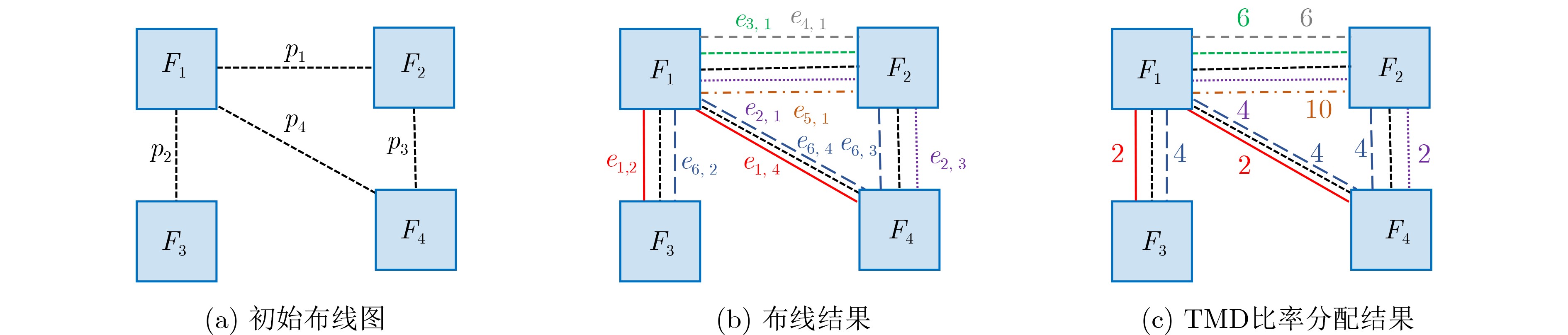
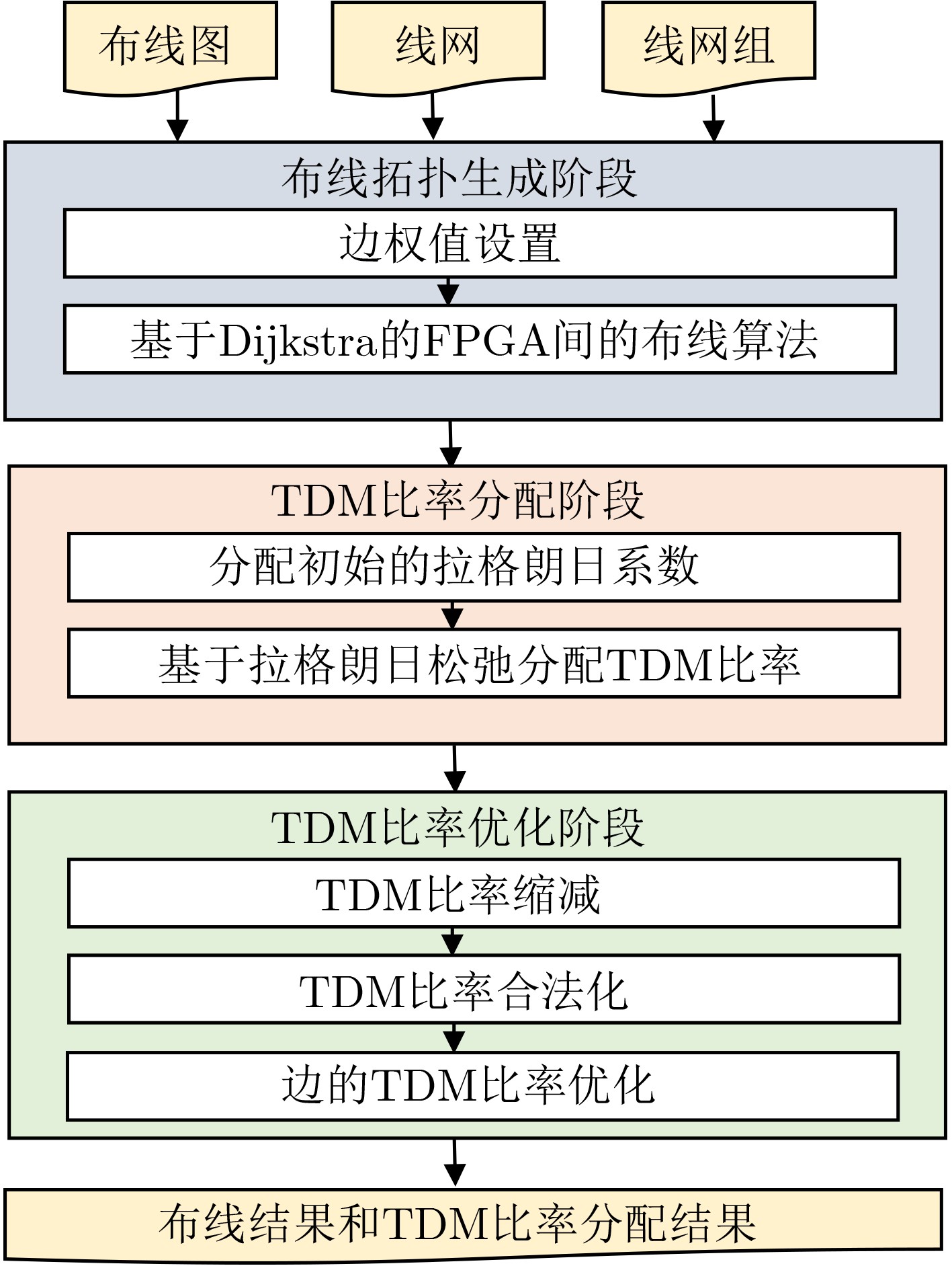
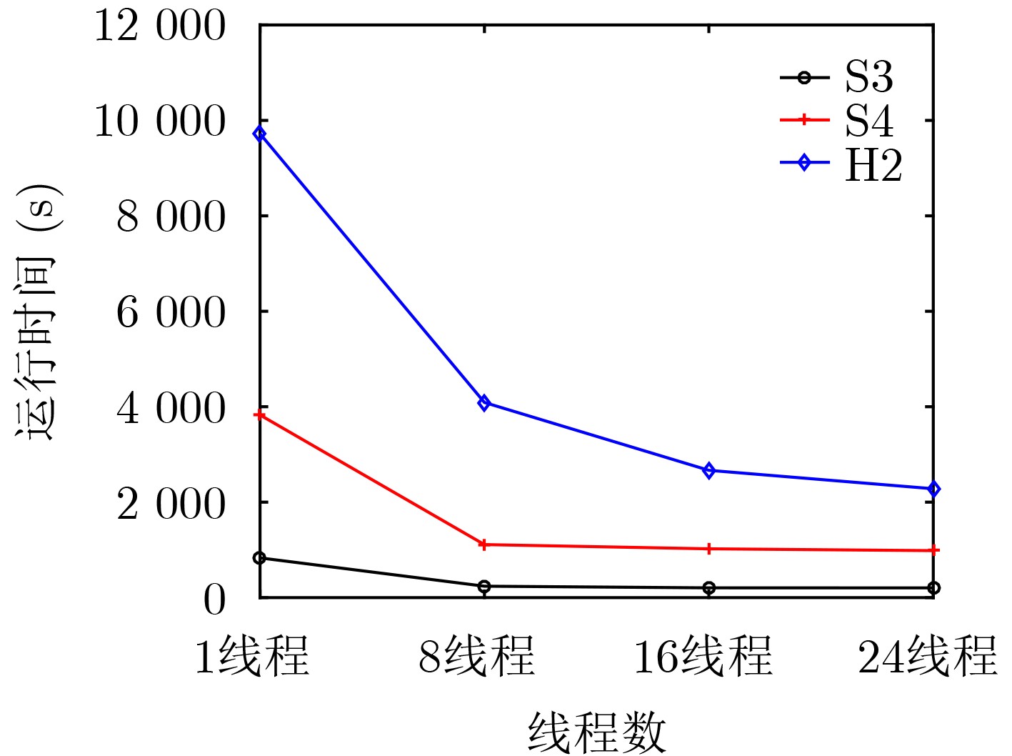
2023, 45(9): 3410-3419. doi: 10.11999/JEIT221420
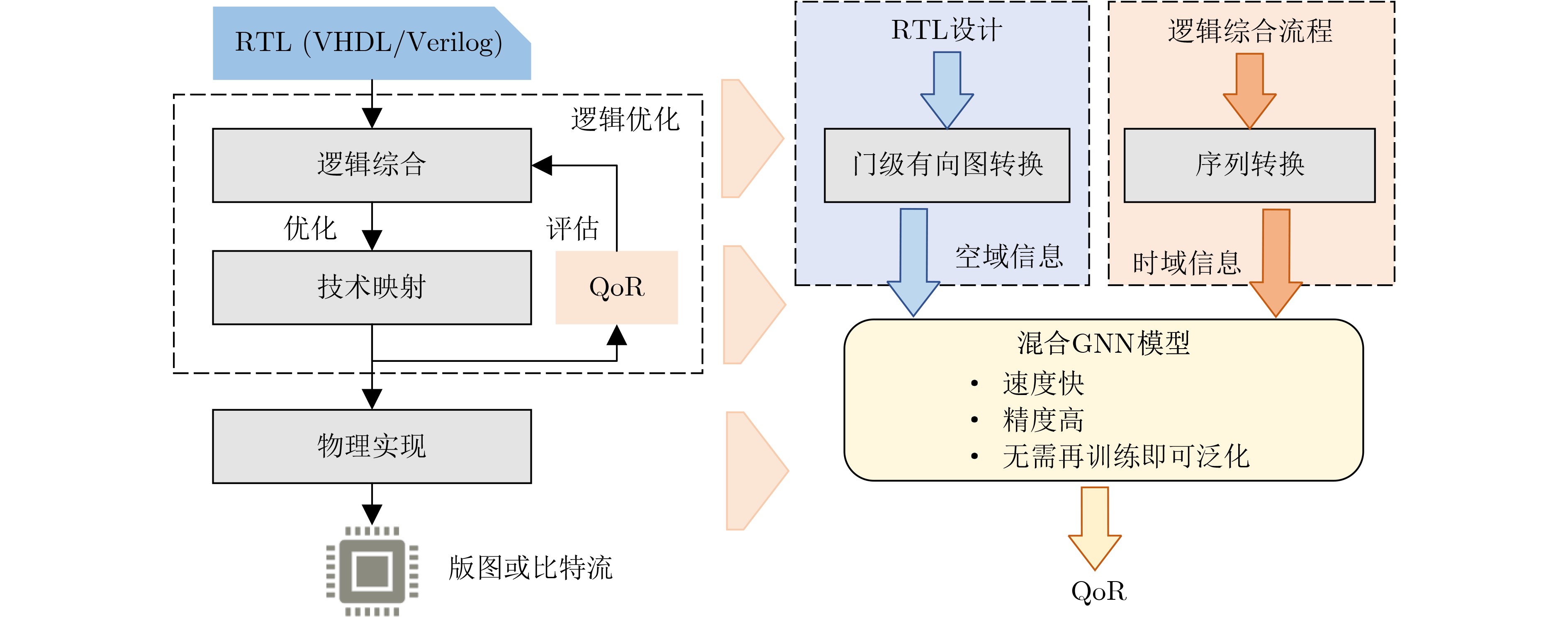
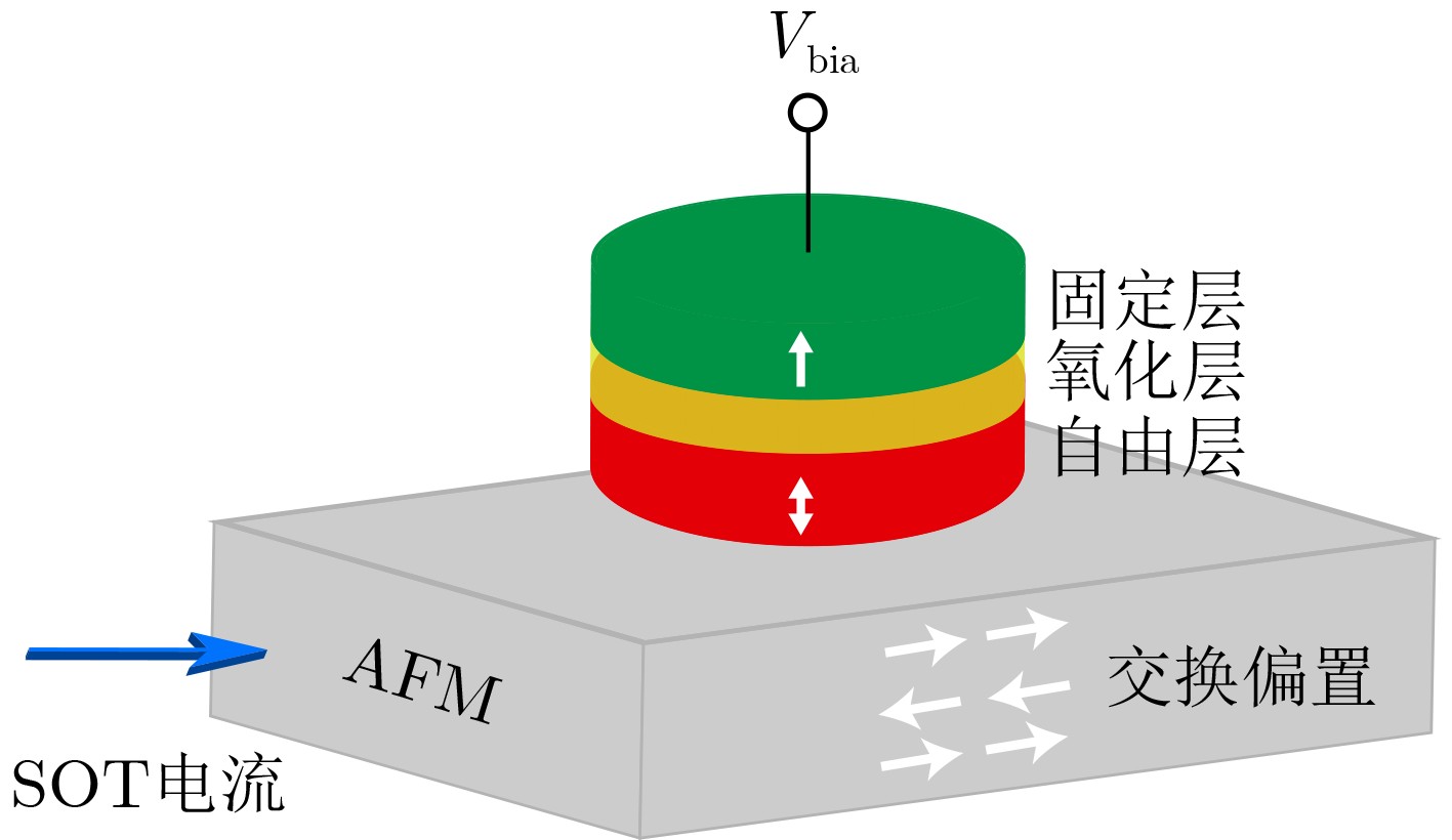
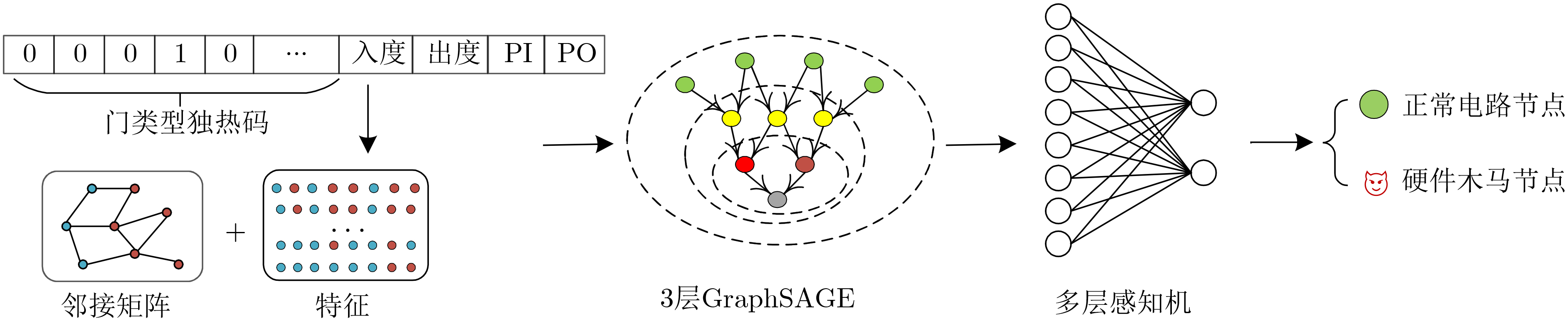
Abstract:
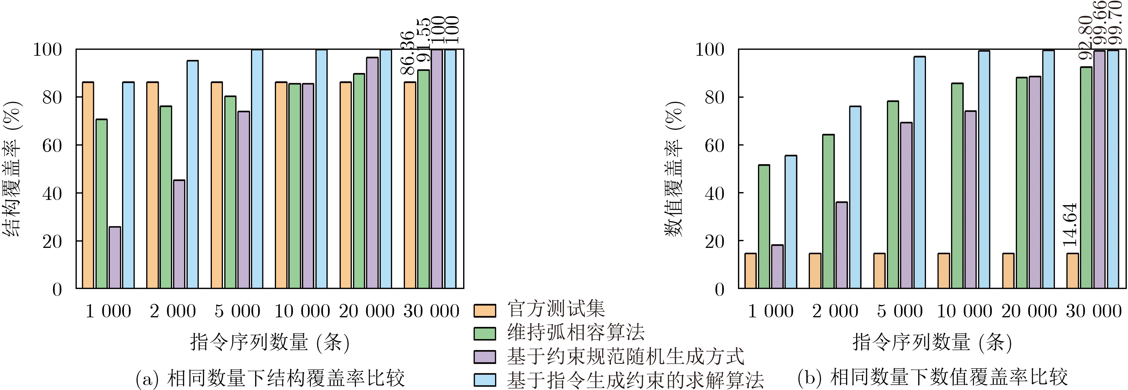
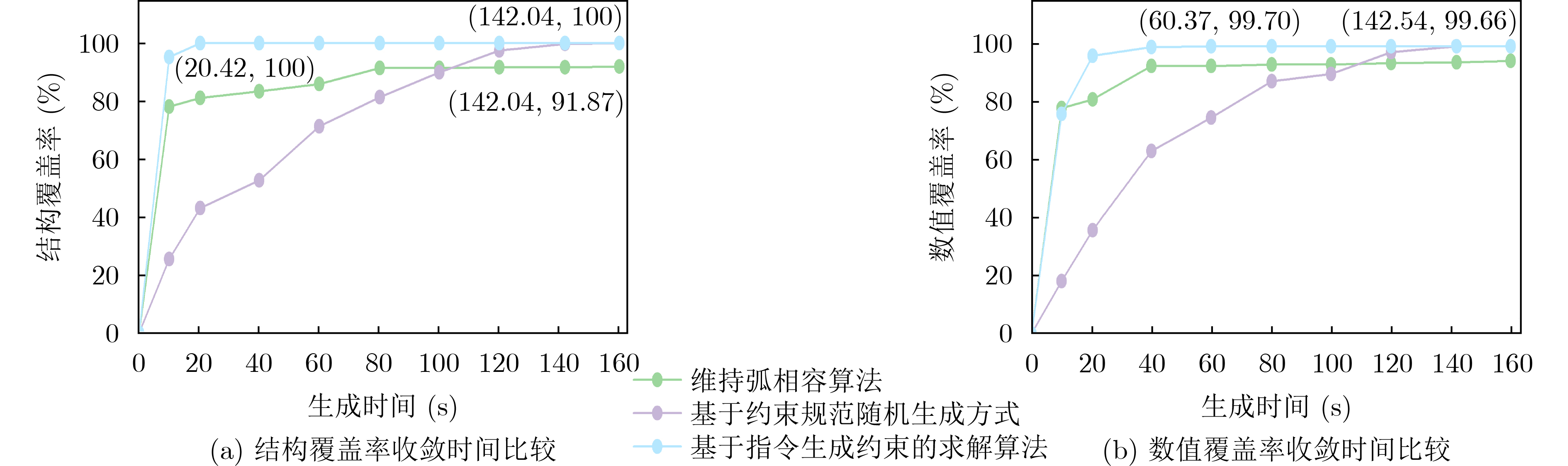
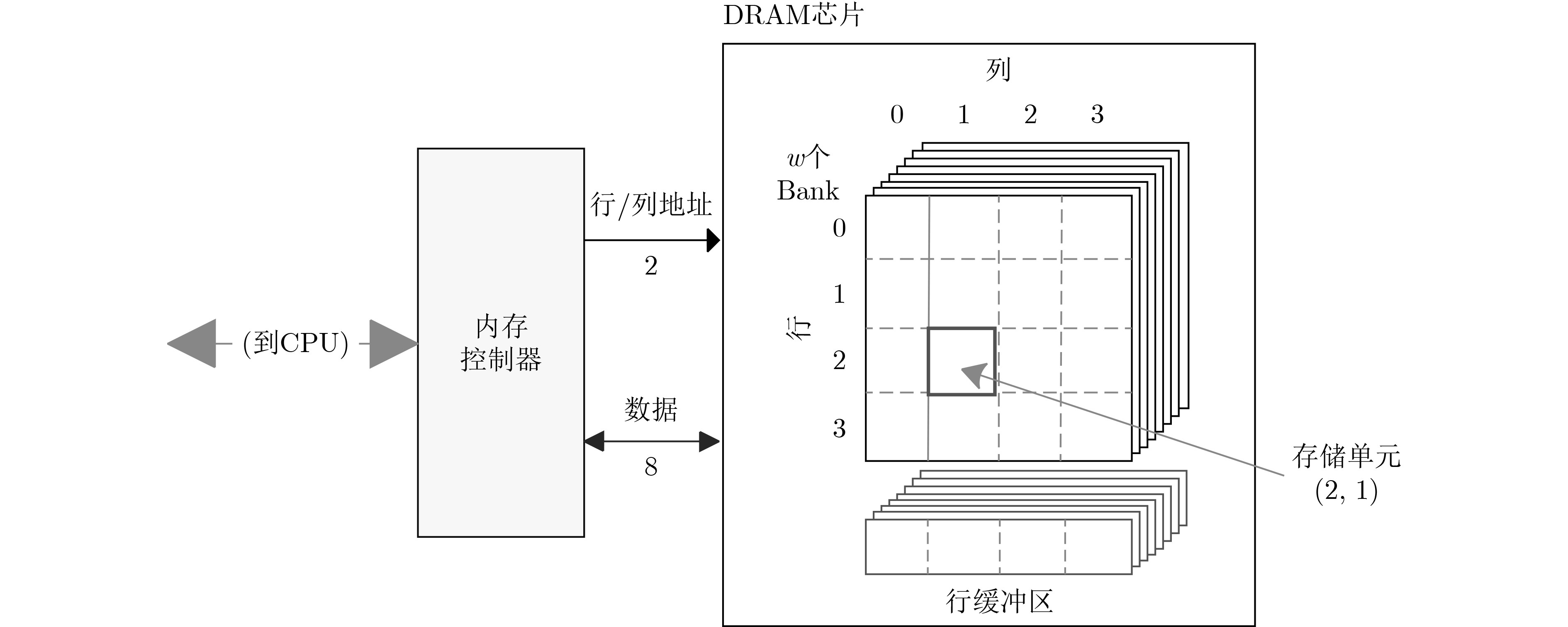
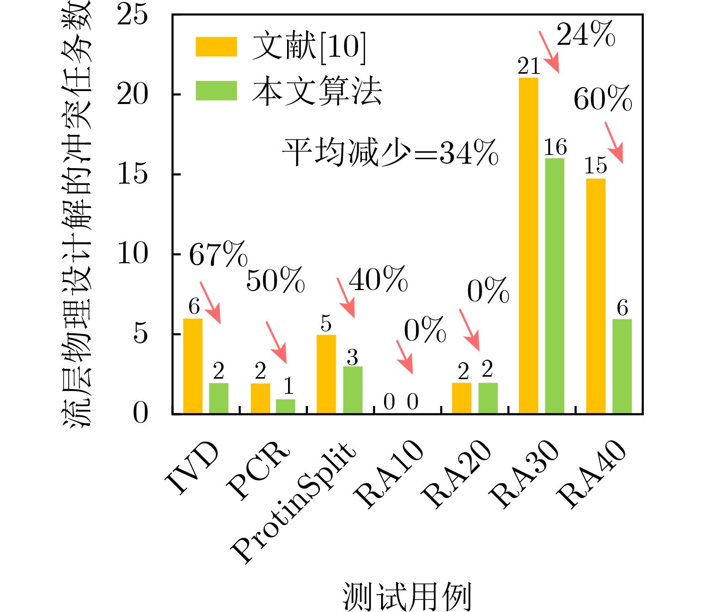
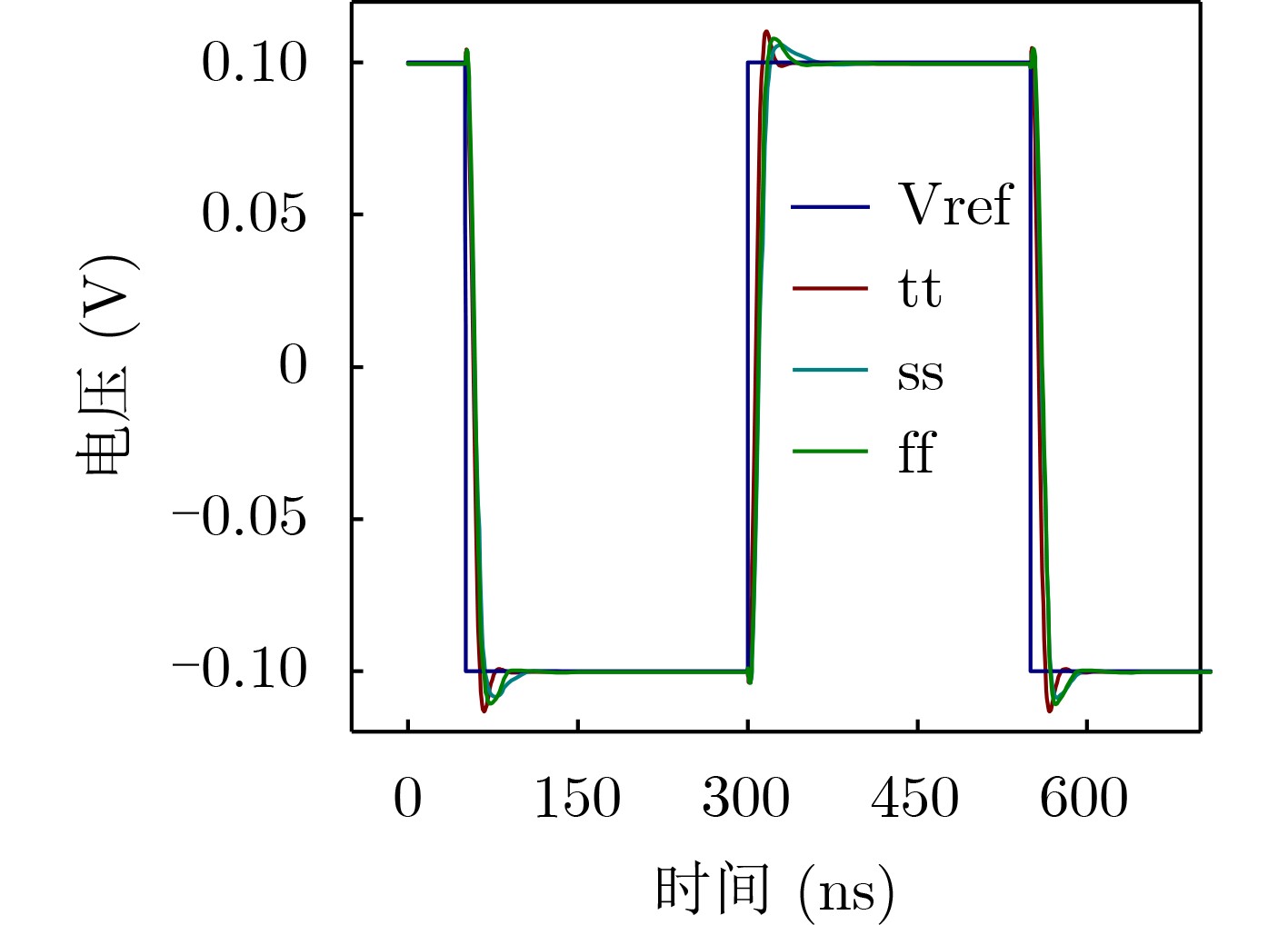
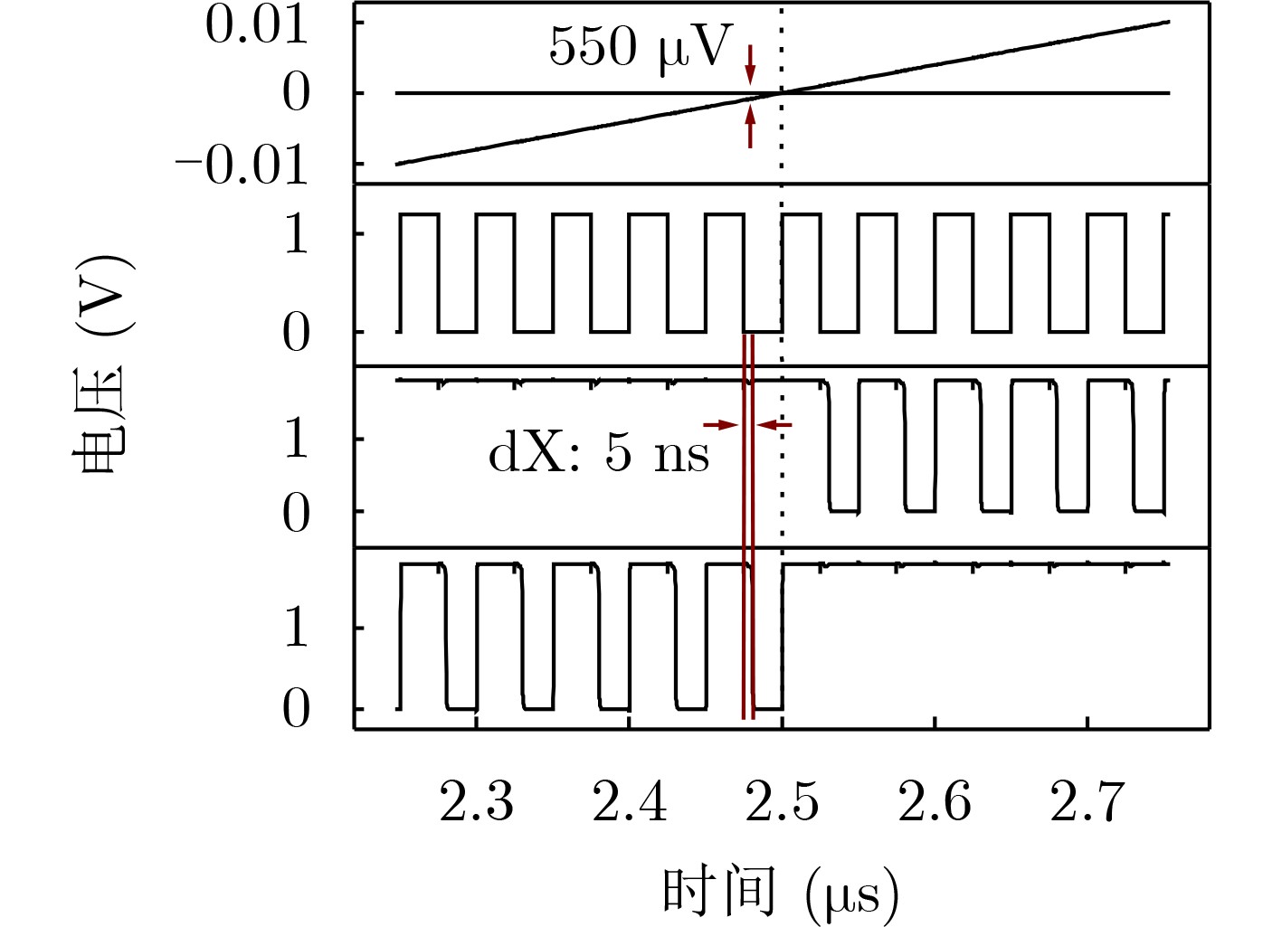
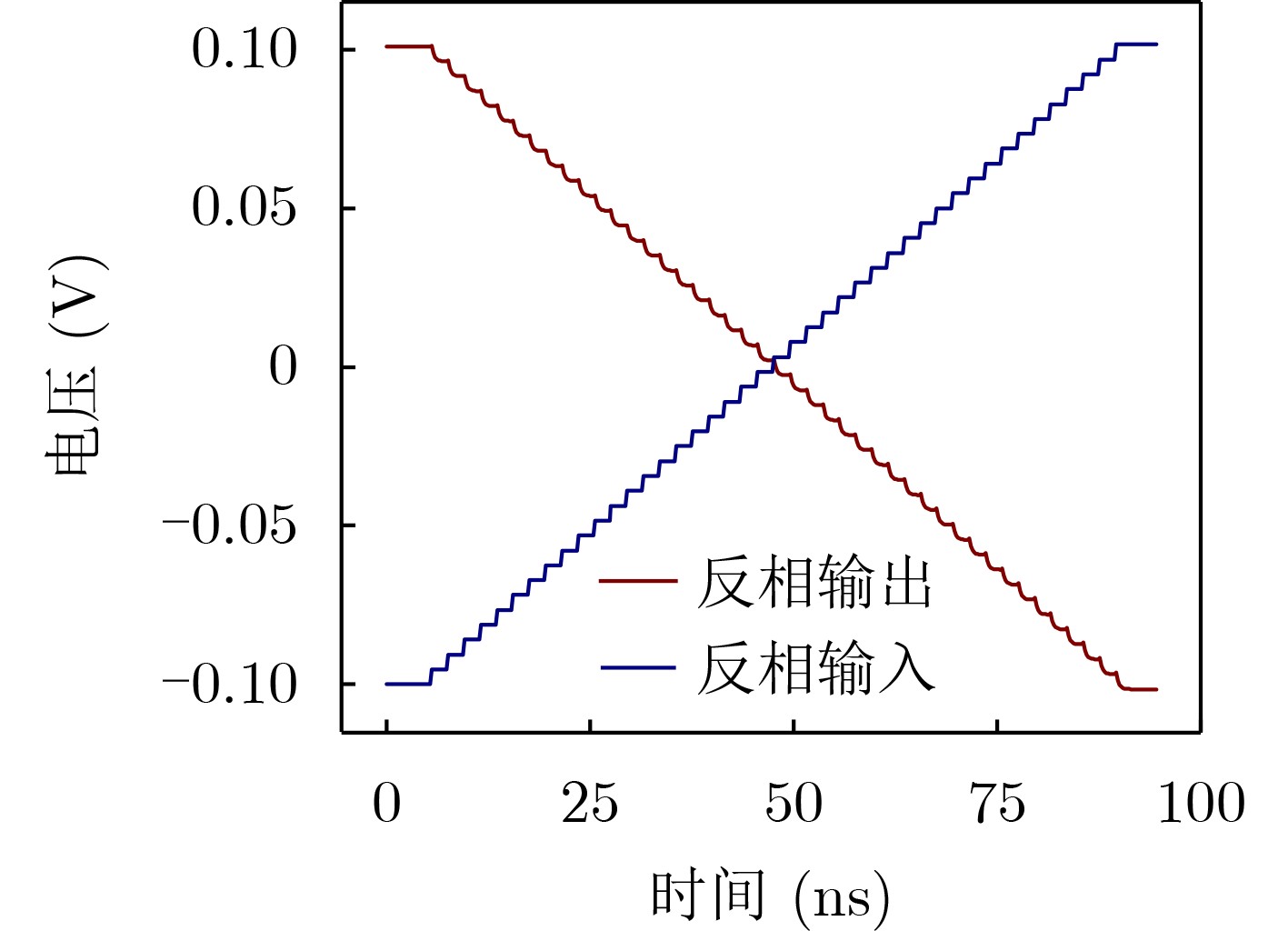
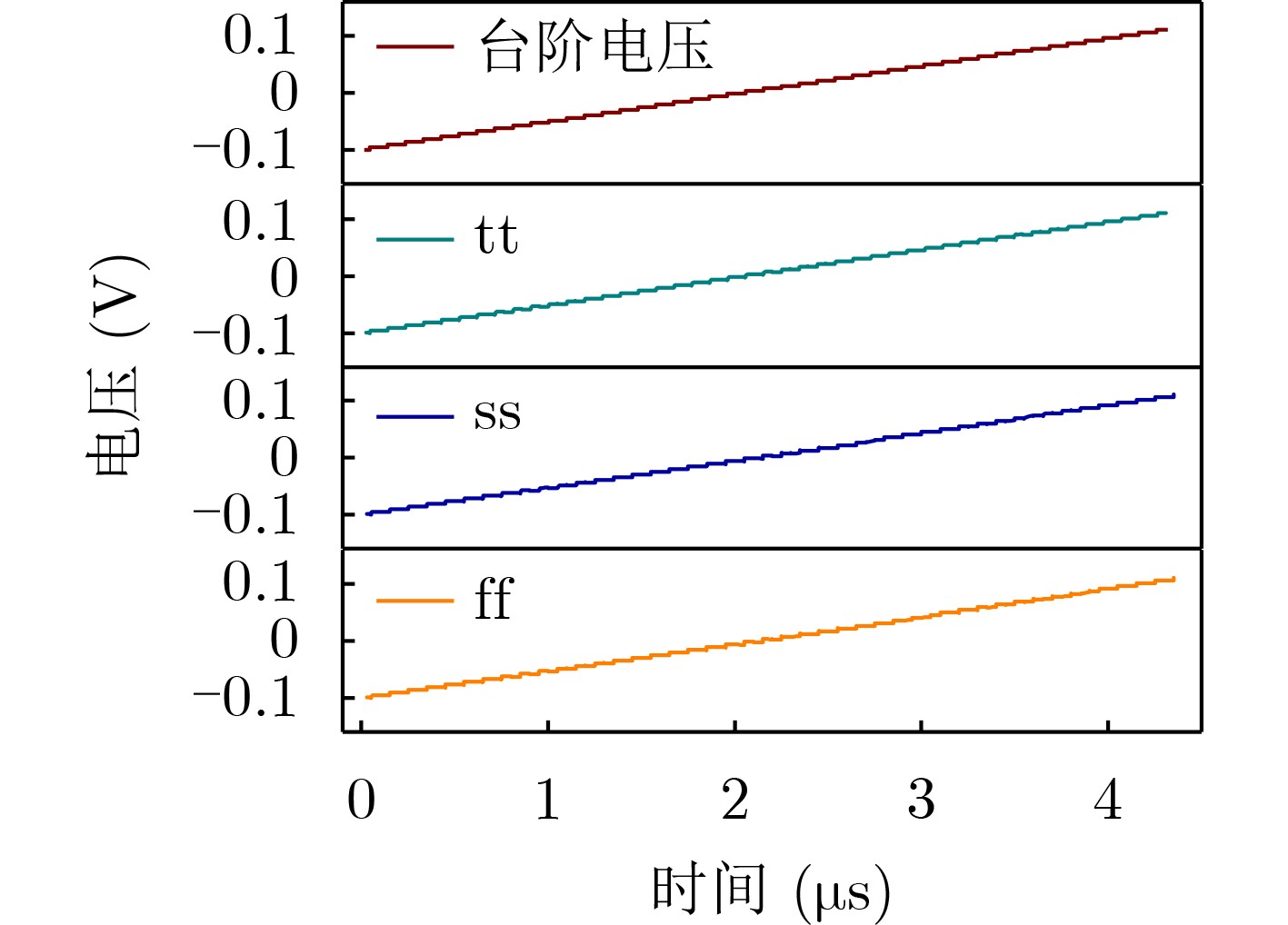
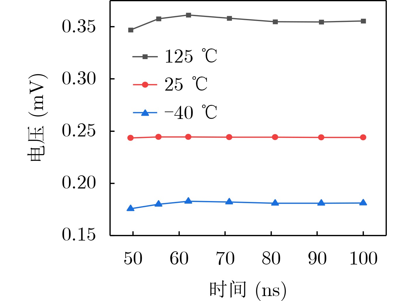
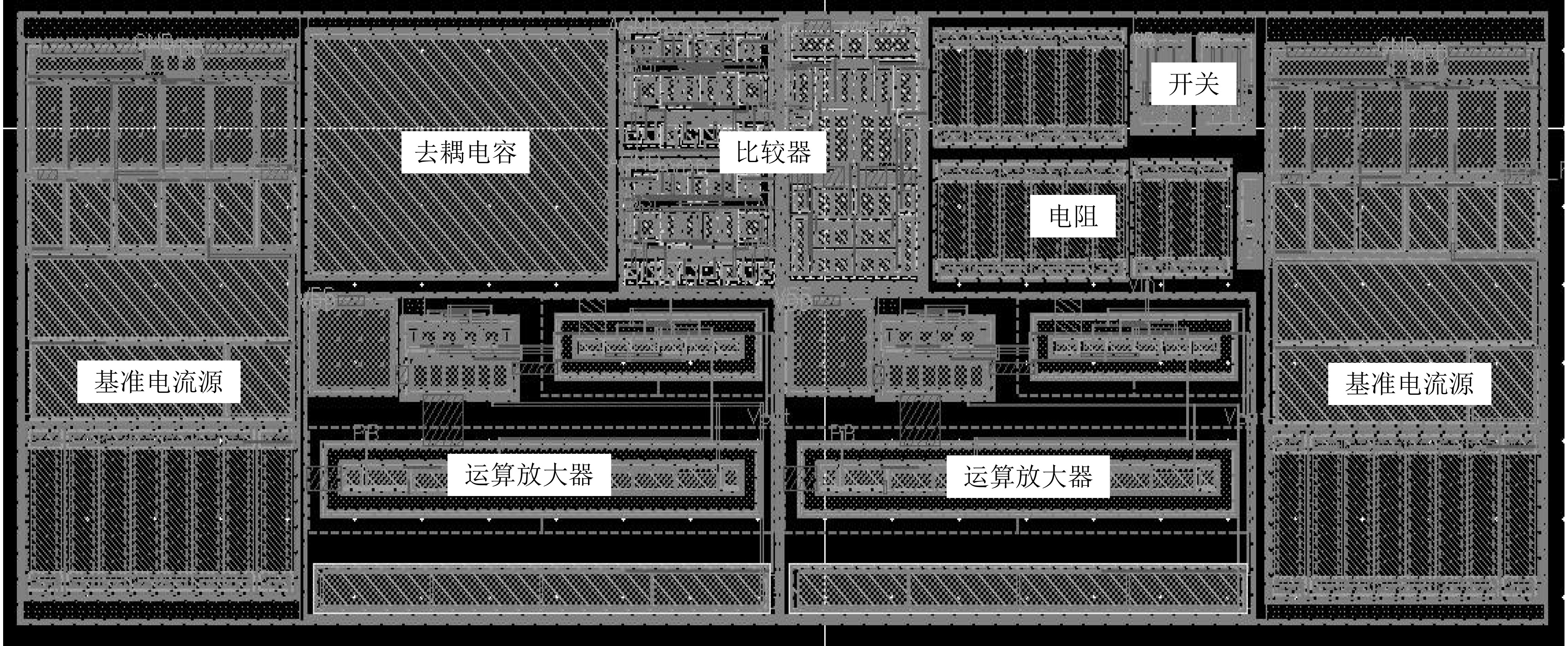
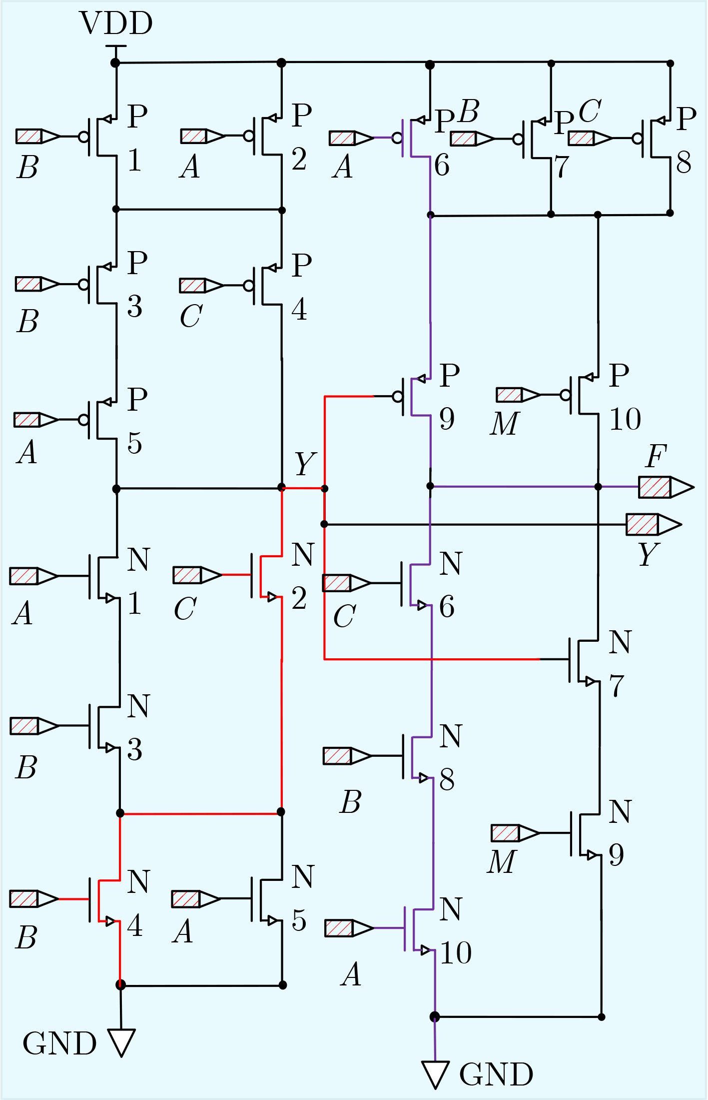
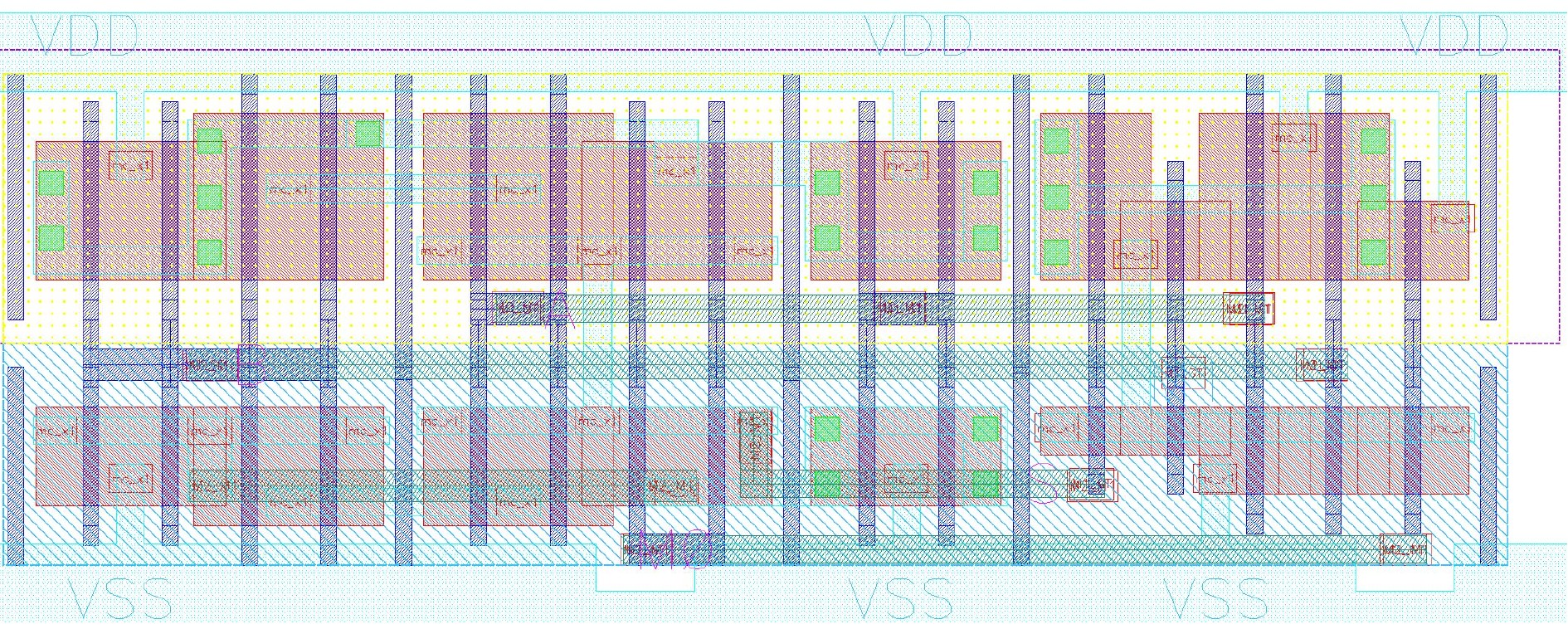
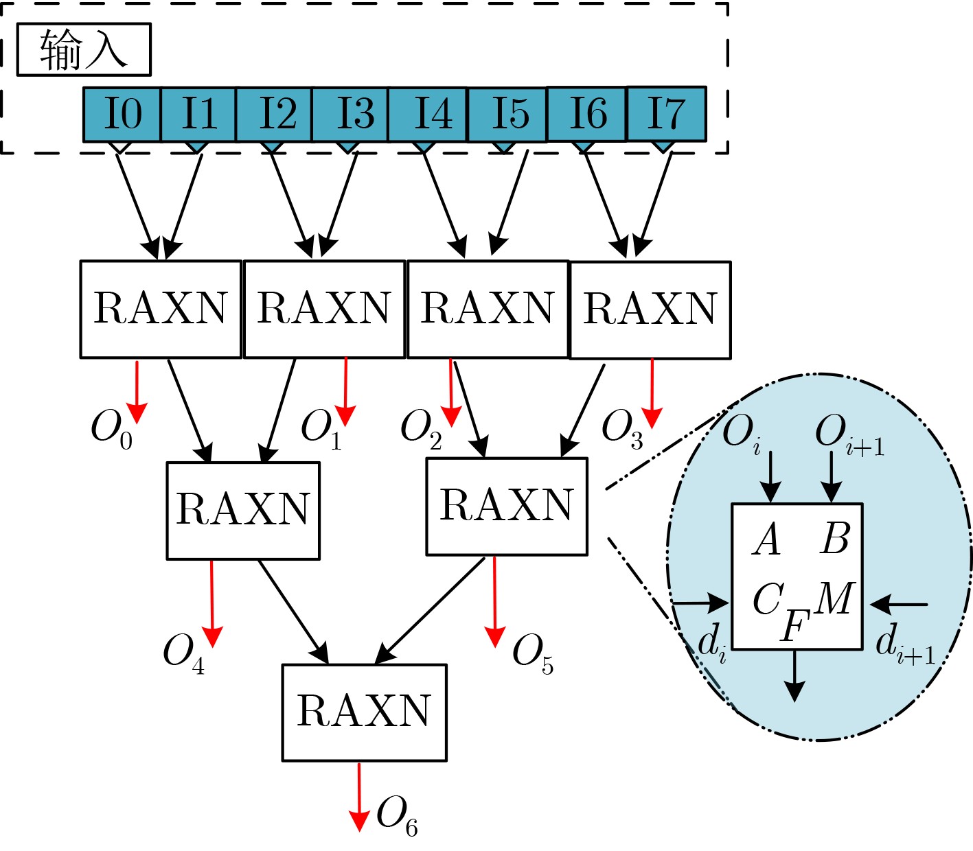
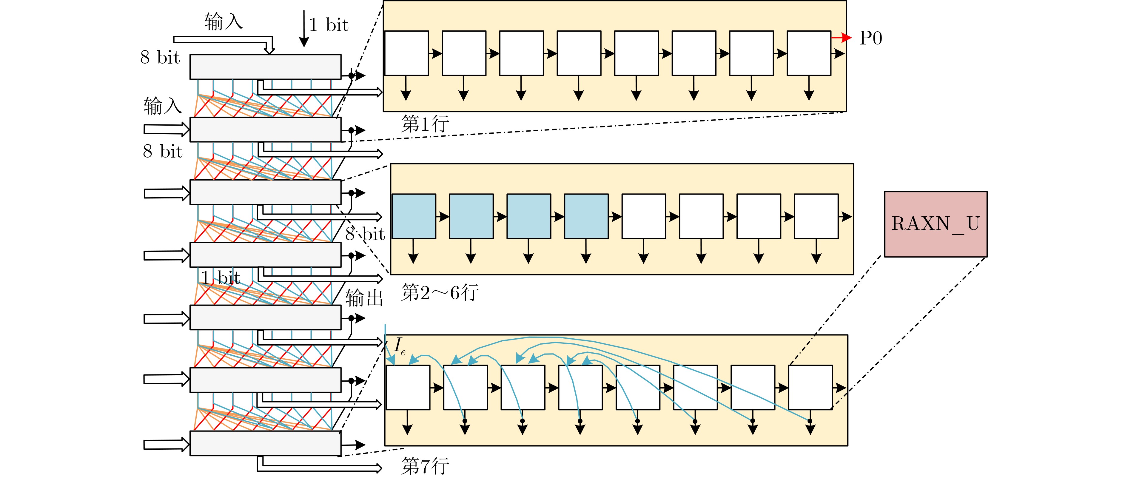
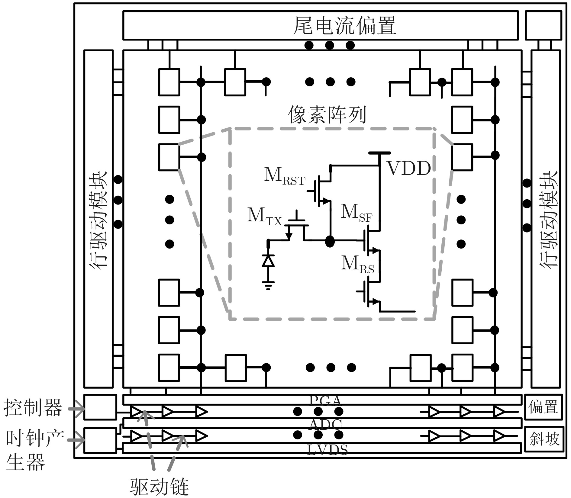
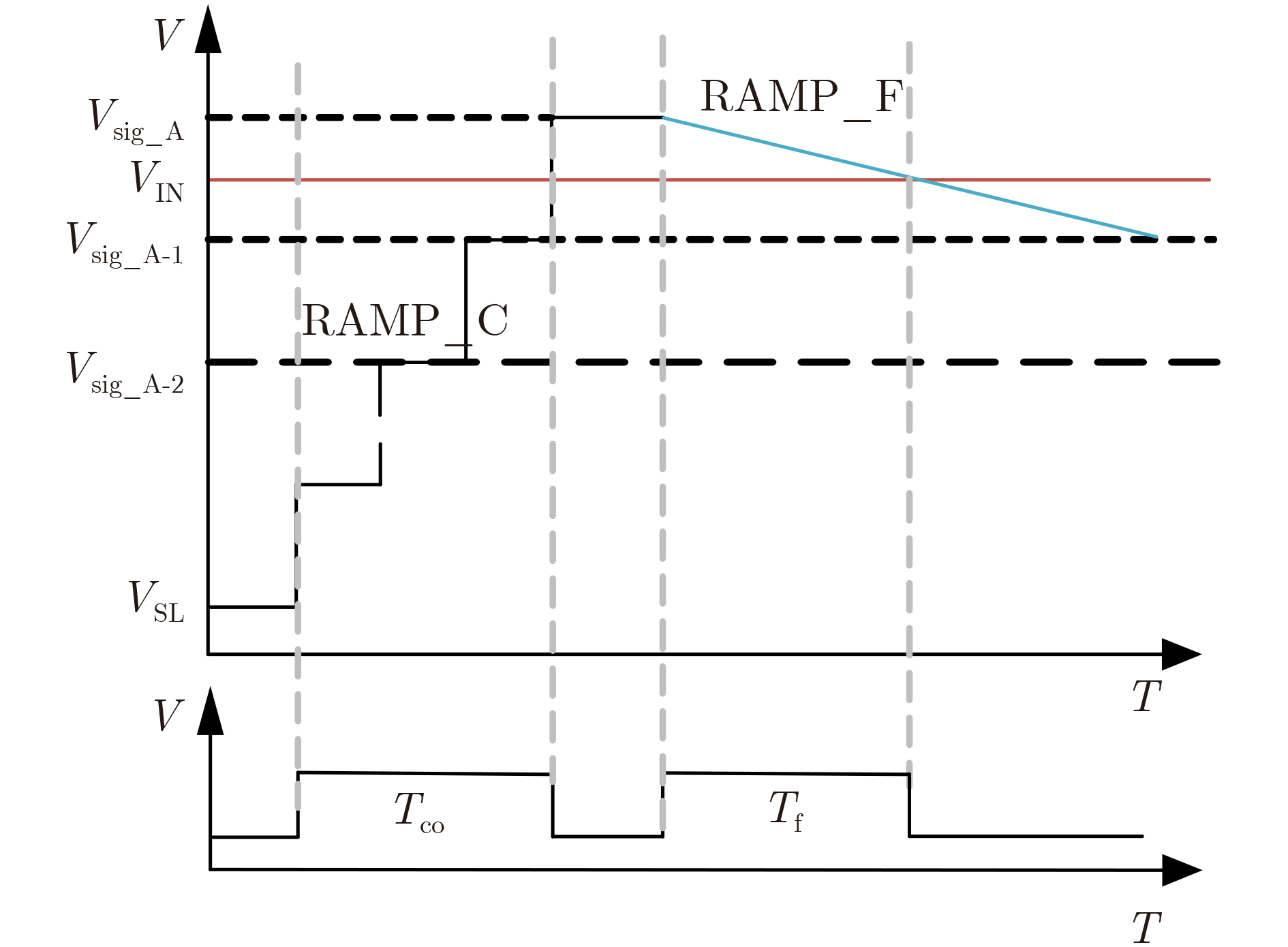
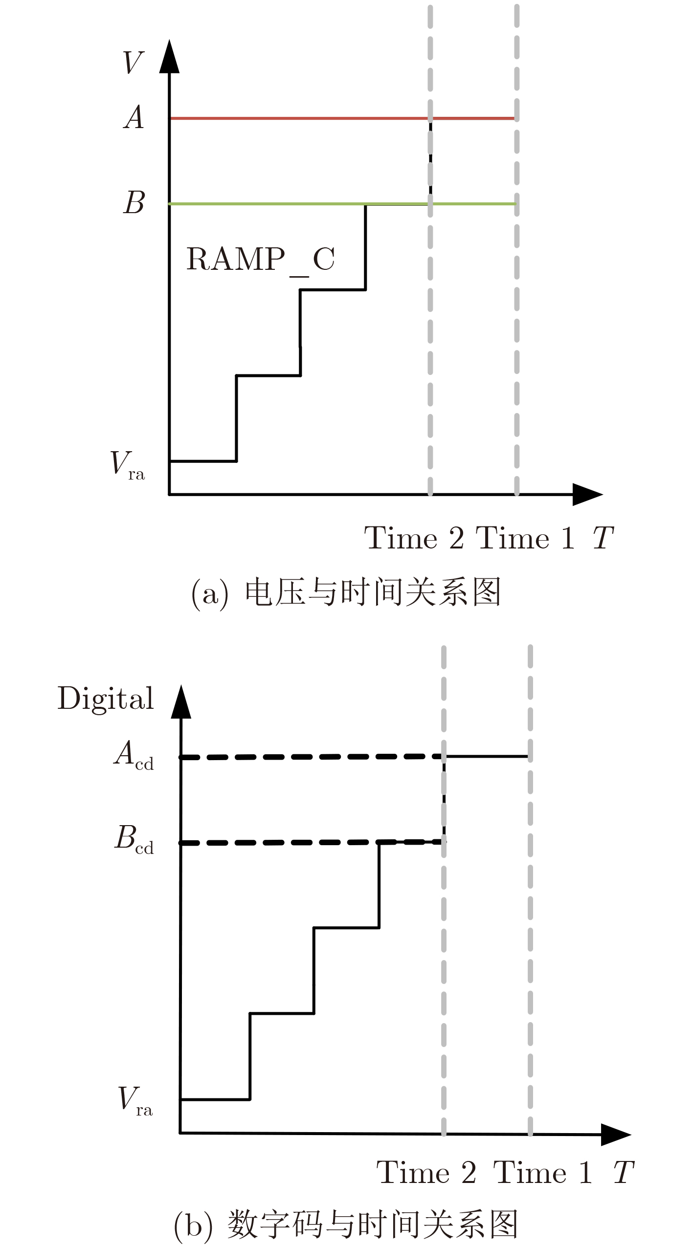
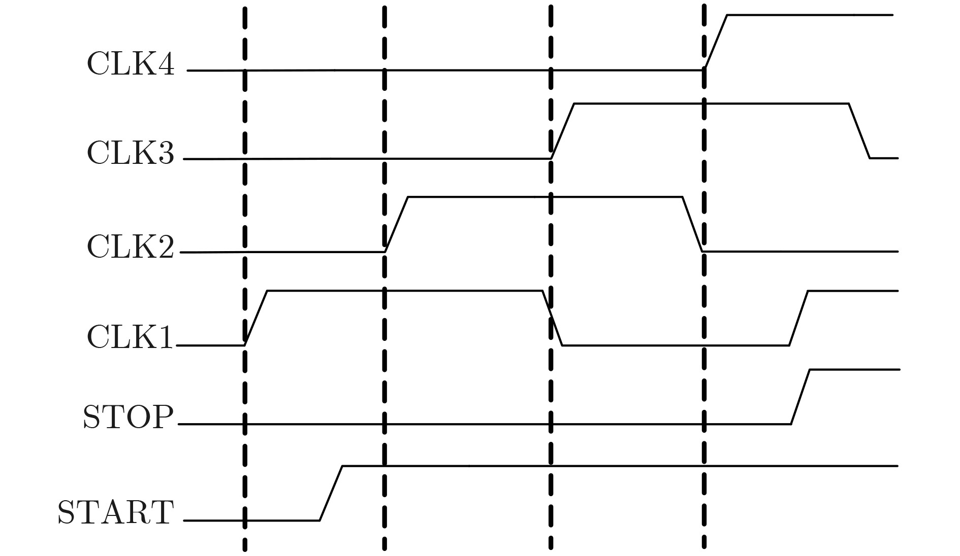
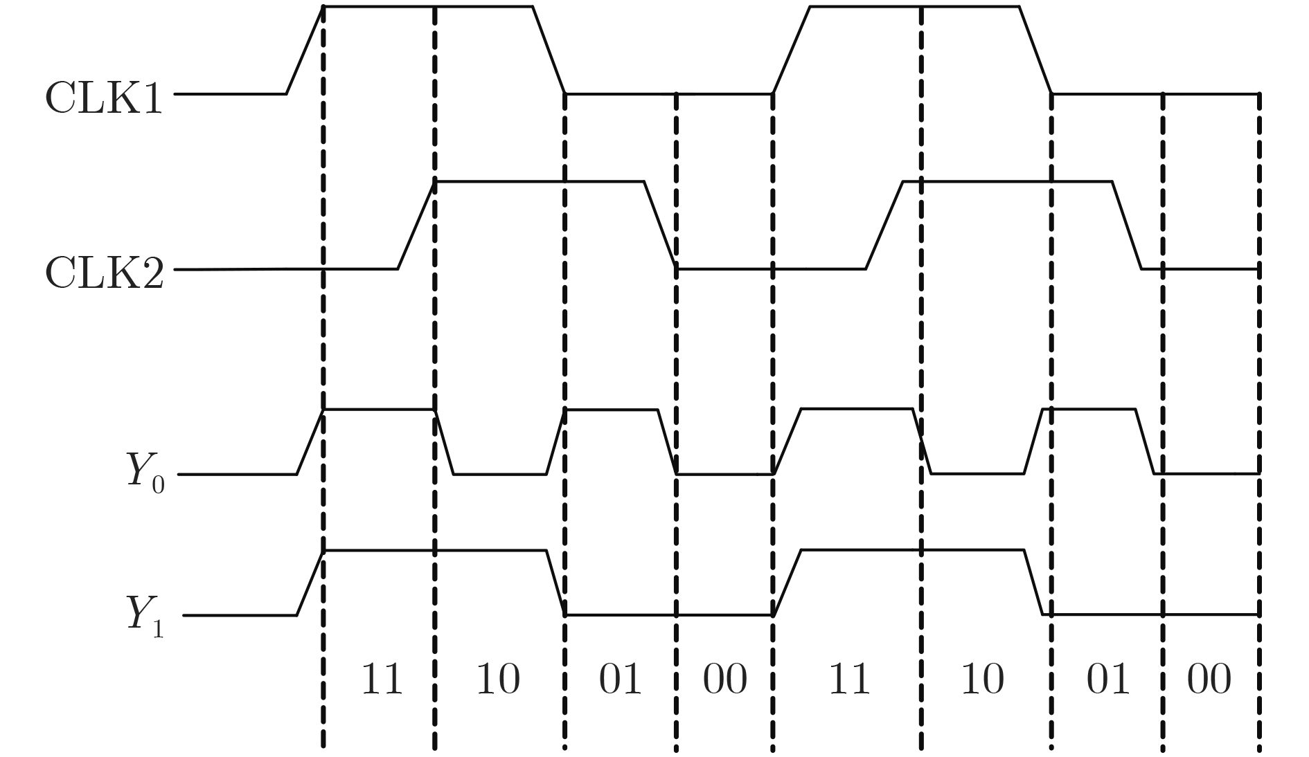
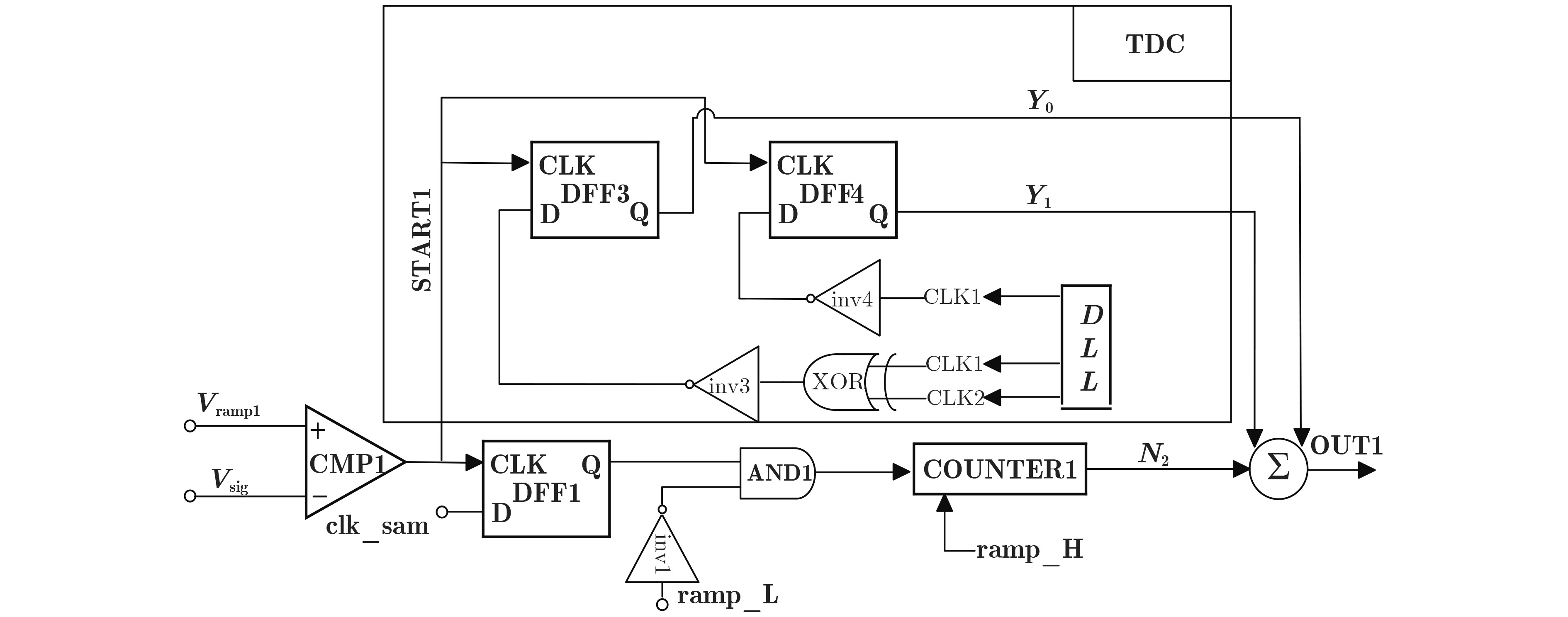
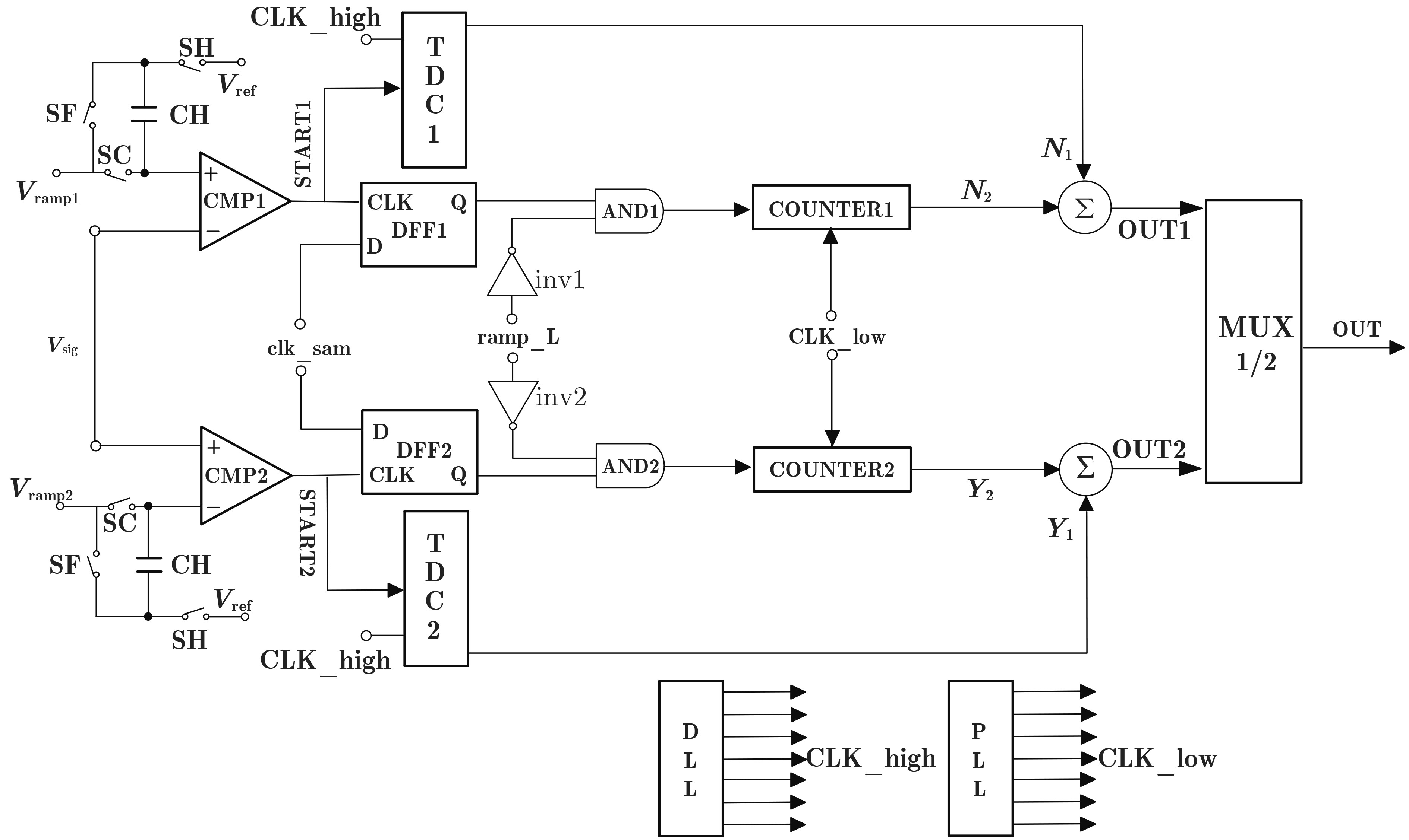
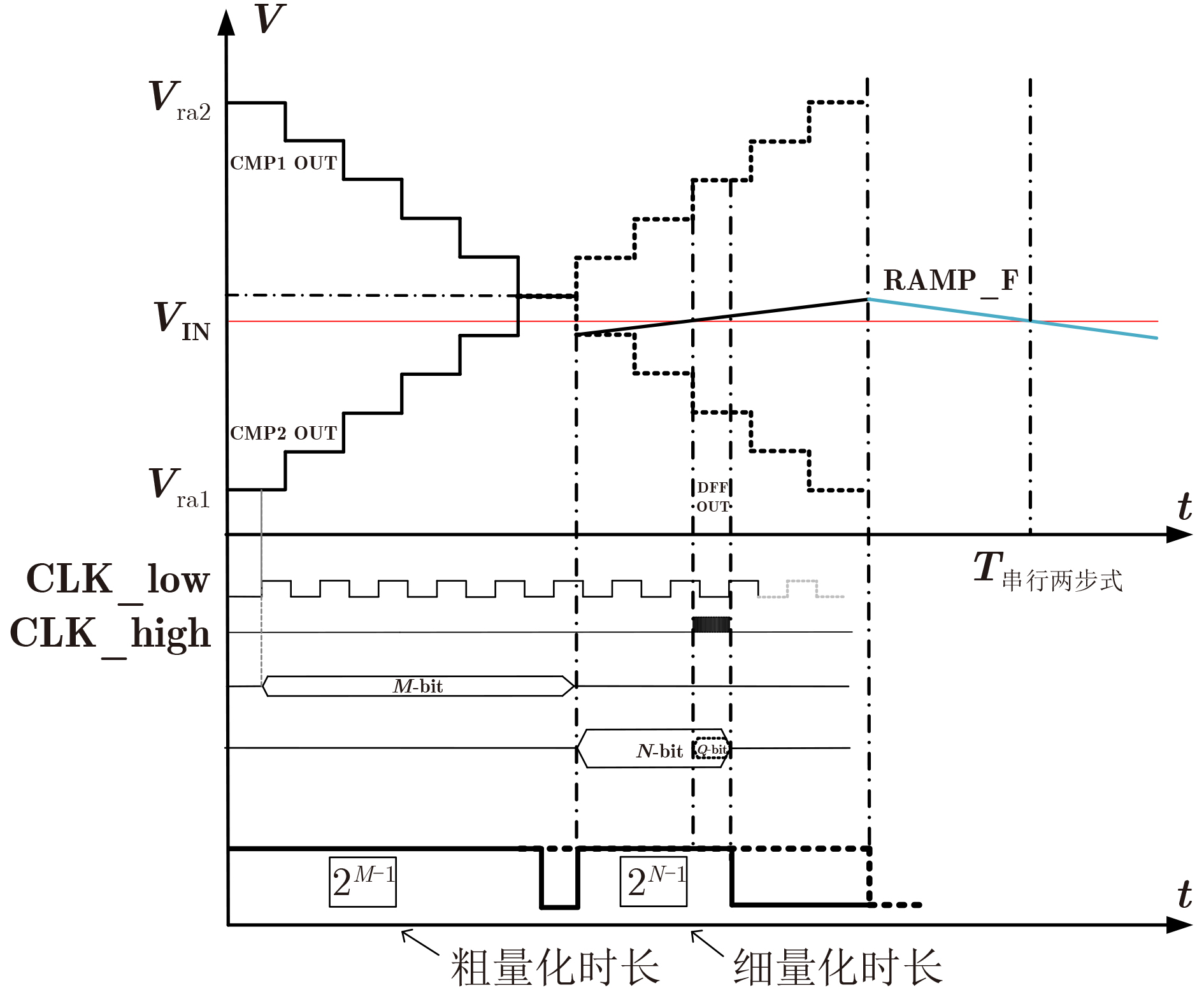
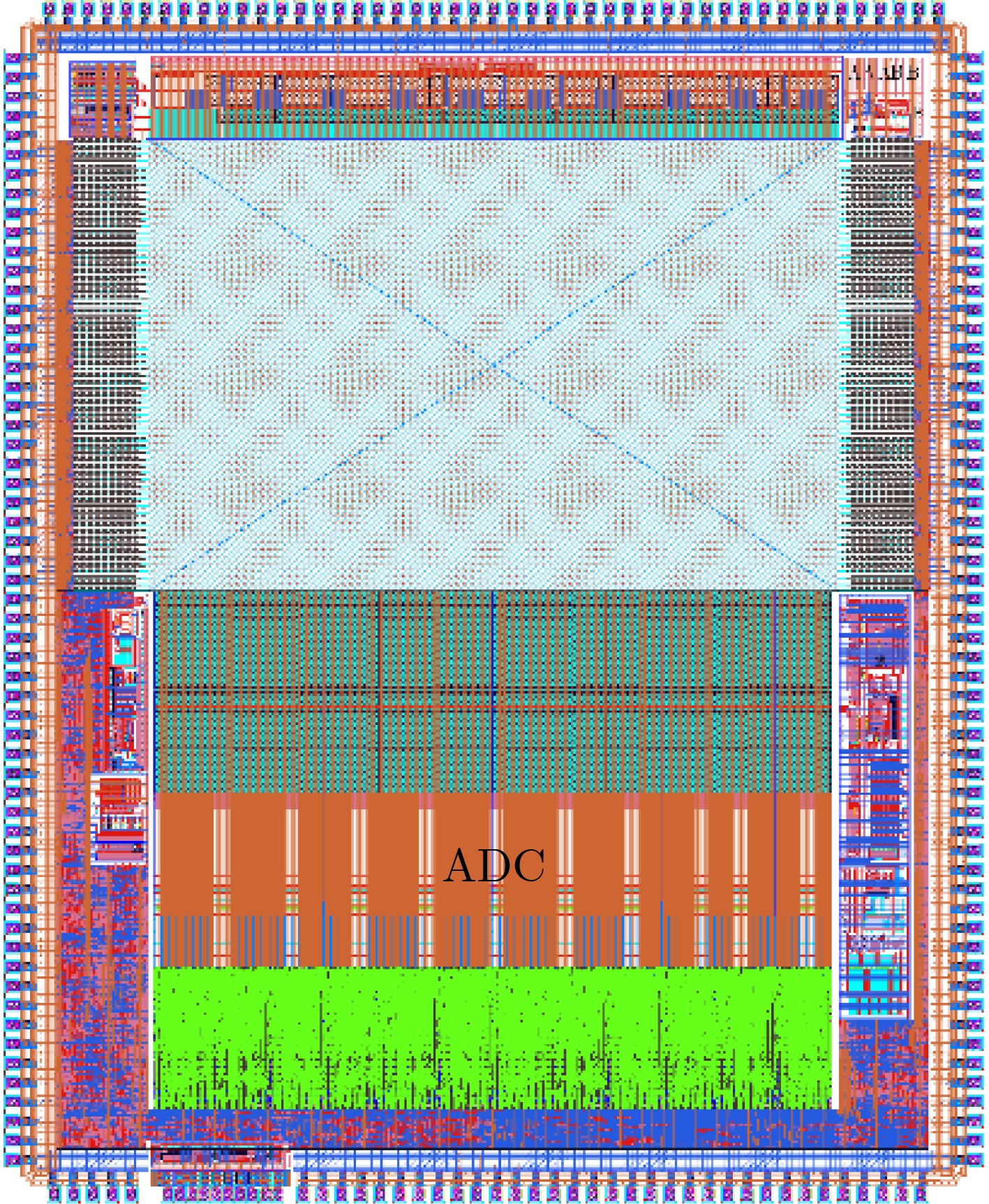
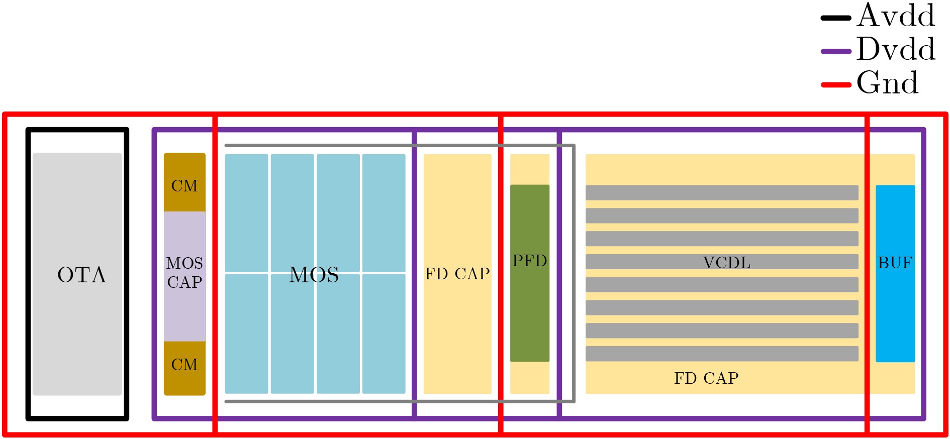
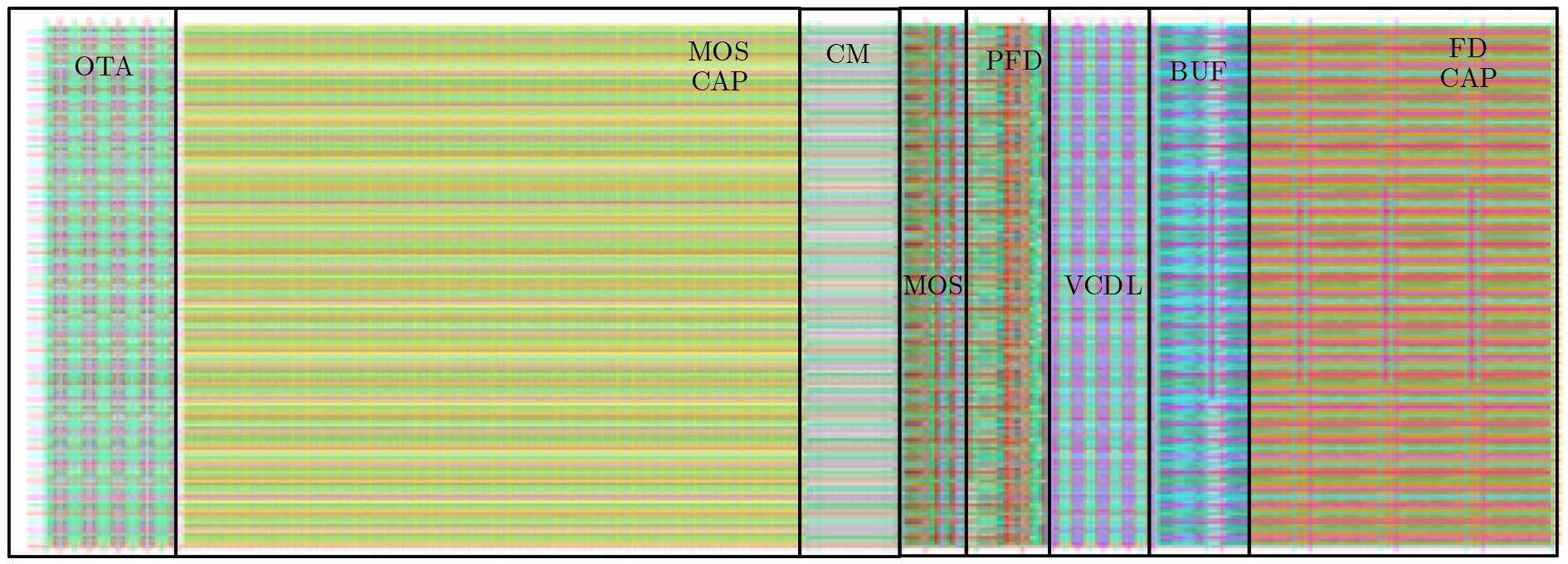
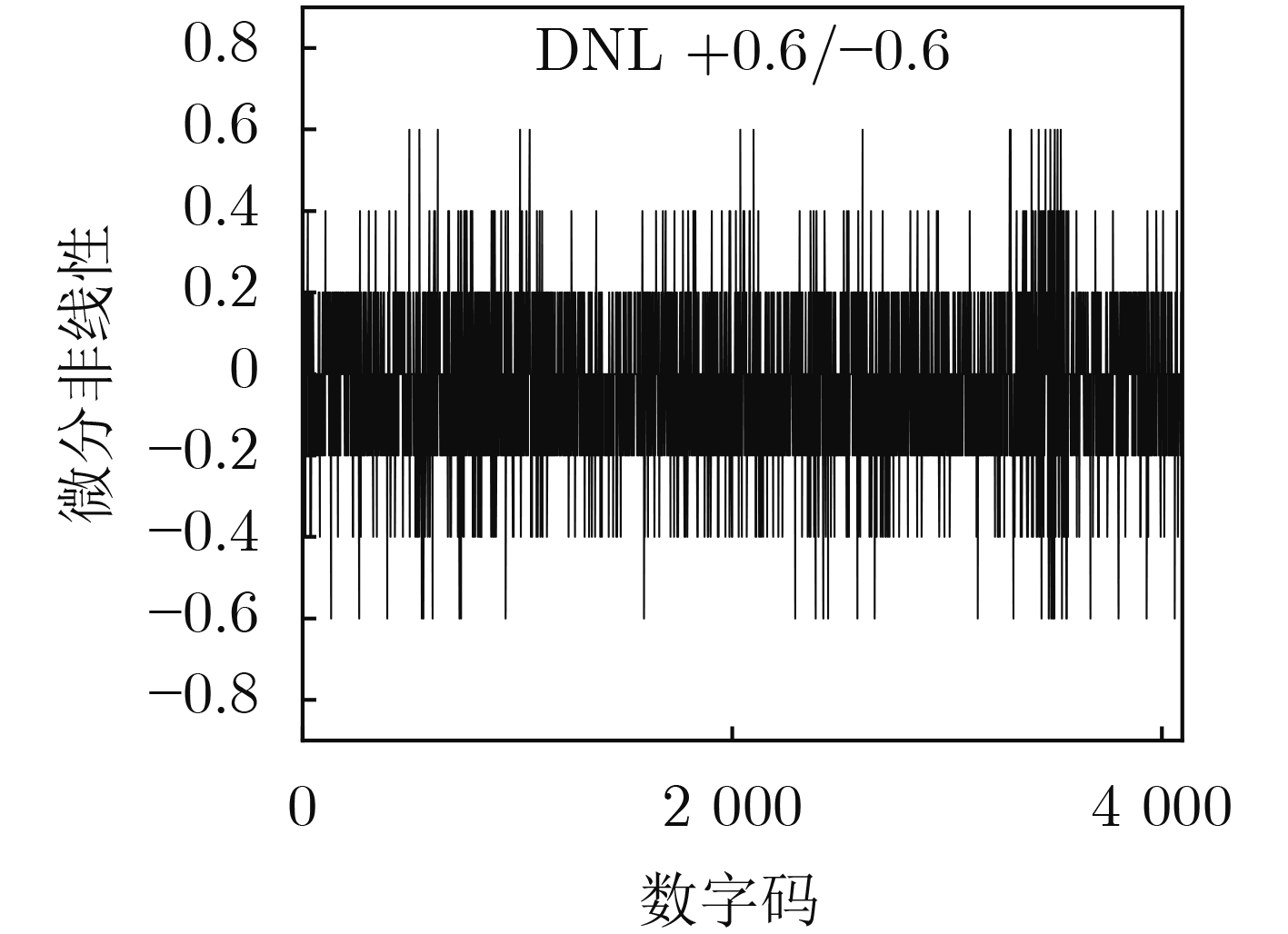
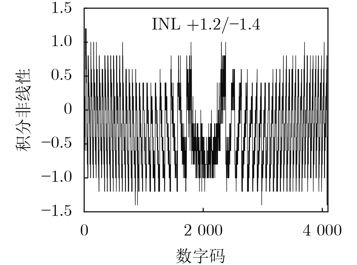
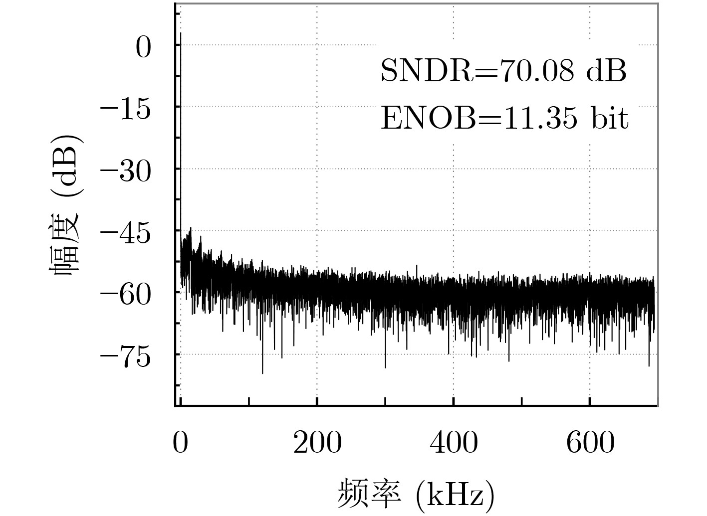
Due to the common speed bottleneck problem of traditional Single-Slope Analog-to-Digital Converter (SS ADC) and serial two-step ADC, the application requirements of high frame rate CMOS Image Sensor (CIS) in the industry have not been met. In this paper, a high-speed fully differential two-step ADC design method for CIS is proposed. The ADC design method is based on differential ramp and Time-to-Digital Conversion (TDC) technology. A parallel conversion mode is formed, which is different from serial conversion, and the robustness of the system is ensured due to the existence of differential ramps. Focusing on the inconsistency between traditional TDC technology and single-slope ADC, a TDC technology based on level coding is proposed, which completes time-to-digital conversion in the last clock cycle of A/D conversion, and realizes a two-step conversion process at another level. Based on the 55 nm 1P4M CMOS experimental platform, this paper completes the circuit design, layout design and test verification of the proposed design method. Under the design environment of analog voltage 3.3 V, digital voltage 1.2 V, clock frequency 100MHz, and dynamic input range 1.6 V, this design is a 12 bit ADC, the conversion time is 480 ns, the column-level power consumption is 62 μW, the DNL (Differential Non-Linearity is measured in the Least Significant Bit) is +0.6/–0.6, the INL (Integral Non-Linearity is measured in the Least Significant Bit) is +1.2/–1.4, and the Signal-to-Noise Distortion Ratio (SNDR) reaches 70.08 dB. Compared with the existing advanced single-slope ADC, the ADC conversion speed is increased by more than 52%, which is a large area array with high frame rate. It provides an effective solution for the implementation of high frame frequency CIS.
Design of Novel Dynamic March Algorithm Based on Memory Built-in Self-test
CAI Zhikuang, YU Haojie, YANG Hang, WANG Zixuan, GUO Yufeng
2023, 45(9): 3420-3429. doi: 10.11999/JEIT221032
Abstract:
As the largest module and one of the most important modules in the System on Chip (SoC), the stability and reliability of memory are related to whether the whole chip can work normally. In order to improve the test efficiency of memory, a novel Dynamic March algorithm—Dynamic-RAWC is proposed. The fault detection effect of the Dynamic-RAWC algorithm is better than that of the classic March RAW algorithm: the dynamic fault coverage is increased by 31.3%. This considerable effect is due to the fact that the test elements of Hammer, March C+ algorithm and some new test elements are integrated into the proposed algorithm which is optimized based on the classic March RAW algorithm. In contrast to ordinary March-type algorithms which have fixed elements, the proposed algorithm supports the user to customize the execution order of the algorithm to meet the detection needs of different faults model, and can dynamically switch the algorithm elements, adjusting between the time complexity and the fault coverage to achieve a good balance.
Multi-Stage Co-Optimization FPGA Routing for Time-Division Multiplexing Technique
LIU Genggeng, XU Wenlin, ZHOU Ruping, XU Ning
2023, 45(9): 3430-3438. doi: 10.11999/JEIT221158
Abstract:
Time-Division Multiplexing (TDM) technology is widely applied to solving the IO limitation problem to improve the routability of FPGA system. However, the increase of the TDM ratio leads to a significant increase in system delay. Therefore, a Multi-Stage Co-Optimization FPGA routing (MSCOFRouting) for Time-Division Multiplexing is proposed in this paper to optimize the system delay and the routability of FPGA system. First, an adaptive routing algorithm is proposed to reduce routing congestion, improve the routability, solve the routing optimization problem between FPGAs, and provide high-quality routing results for subsequent TDM ratio assignment. Second, to avoid the delay degradation caused by excessive TDM ratio of large-scale net groups, a TDM ratio assignment algorithm based on Lagrangian relaxation is utilized to assign the initial TDM ratio with a smaller delay to the edge distribution system of the routing graph. In addition, a multi-level TDM ratio optimization algorithm is used to reduce the TDM ratios of the net group with maximum TDM ratios. The TDM ratio reduction is employed for the net group and the FPGA connection pair. Meanwhile, a multi-thread parallelization method is integrated into the three algorithms above to improve further the efficiency of MSCOFRouter. Experiments show that MSCOFRouting can obtain the results satisfying the TDM ratio constraint, and achieve the best routing optimization results and TDM ratio assignment results.