

基于双侧P型柱与电流扩展层协同设计的1200 V沟槽型SiC MOSFET性能优化与栅氧电场分析
doi: 10.11999/JEIT260164 cstr: 32379.14.JEIT260164
Performance Optimization and Gate Oxide Electric Field Analysis of 1200V Trench SiC MOSFET Based on PCL-CSL Collaborative Design
-
摘要: 碳化硅(SiC)功率金属-氧化物-半导体场效应晶体管(MOSFET)凭借耐压高、导通电阻低和功耗小的优势,已广泛应用于中高压电力电子系统中,在提升系统效率与功率密度方面具有重要意义。该文基于TCAD仿真平台,开展
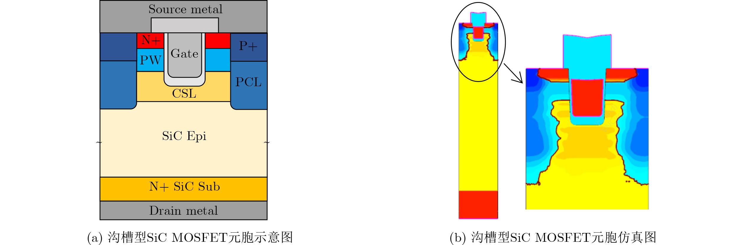
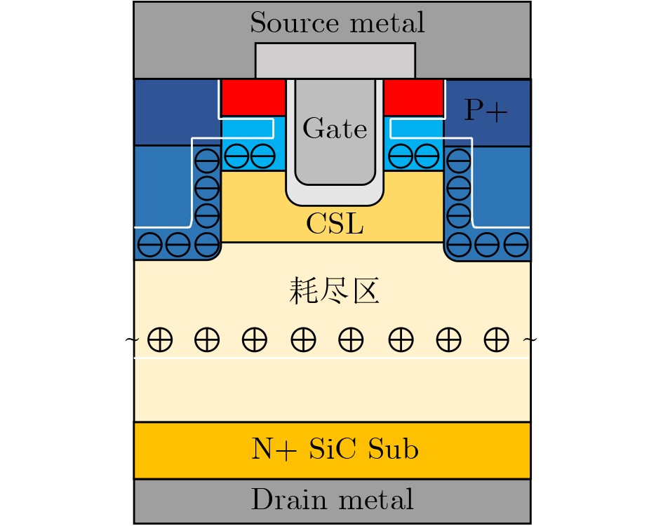
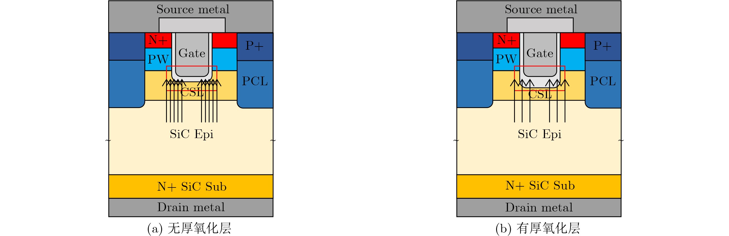
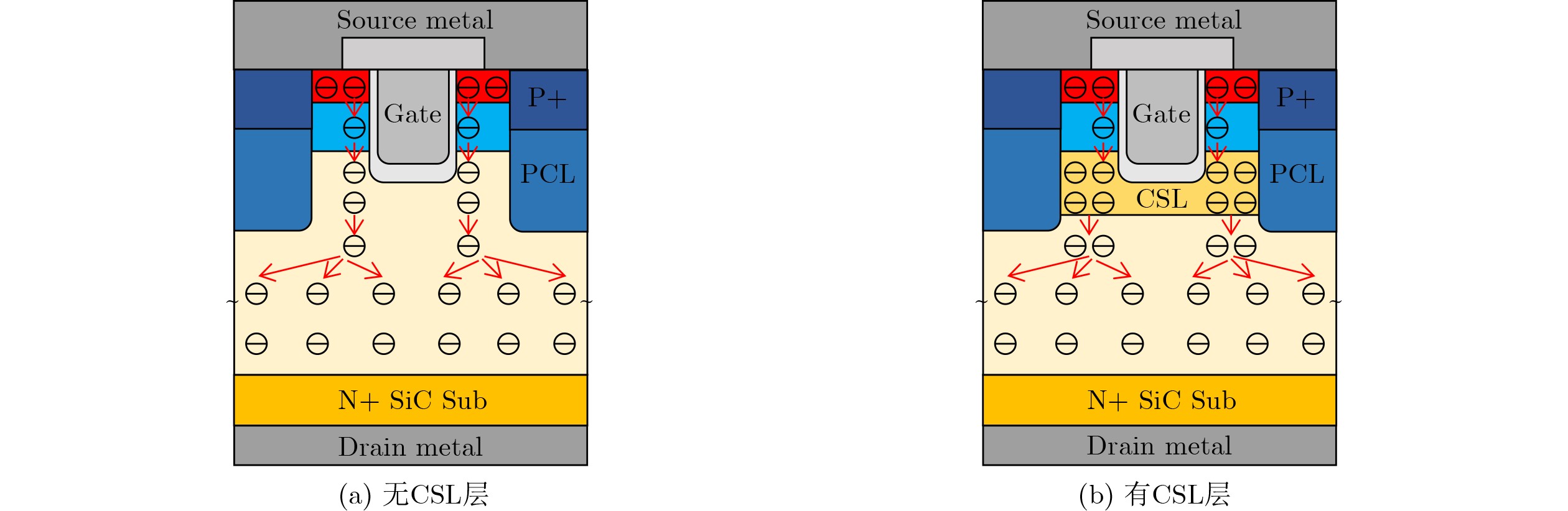
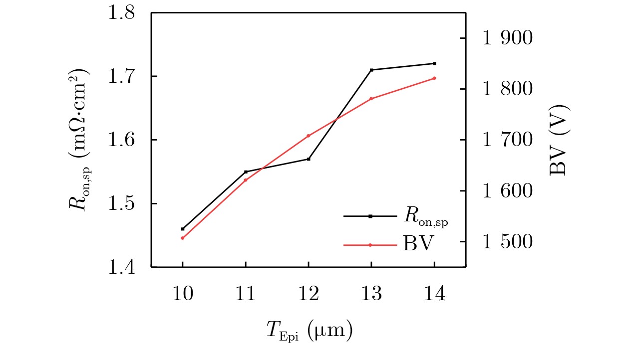
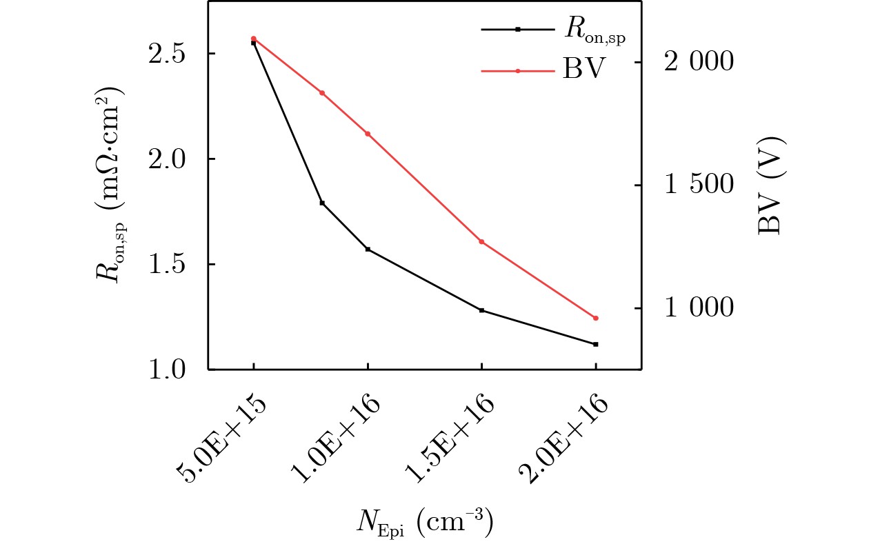
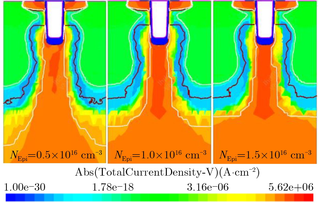
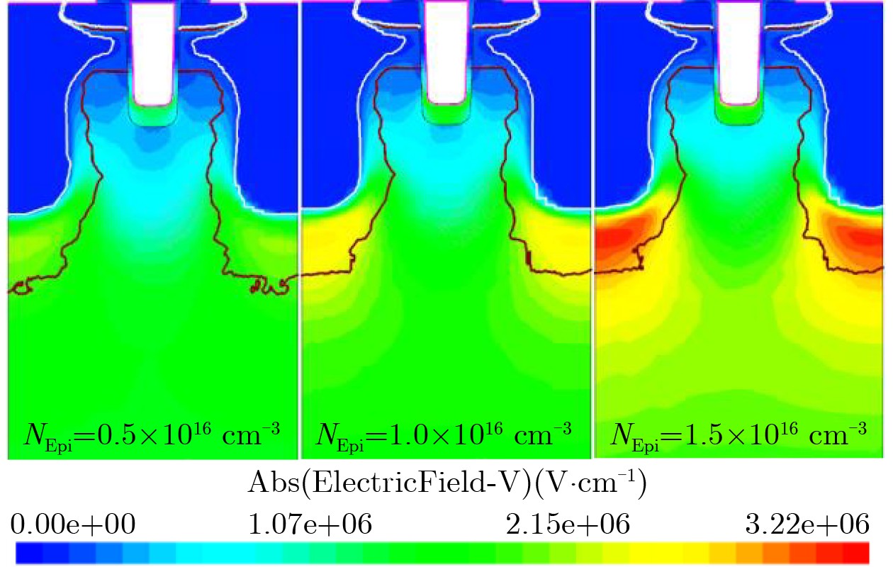
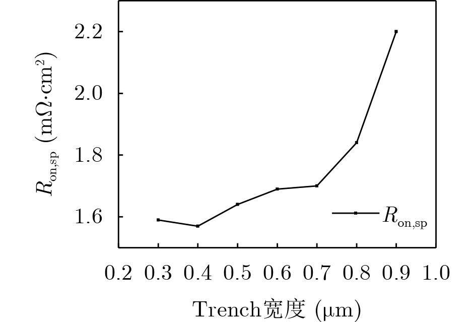
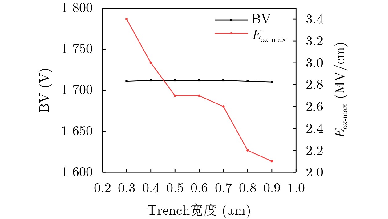
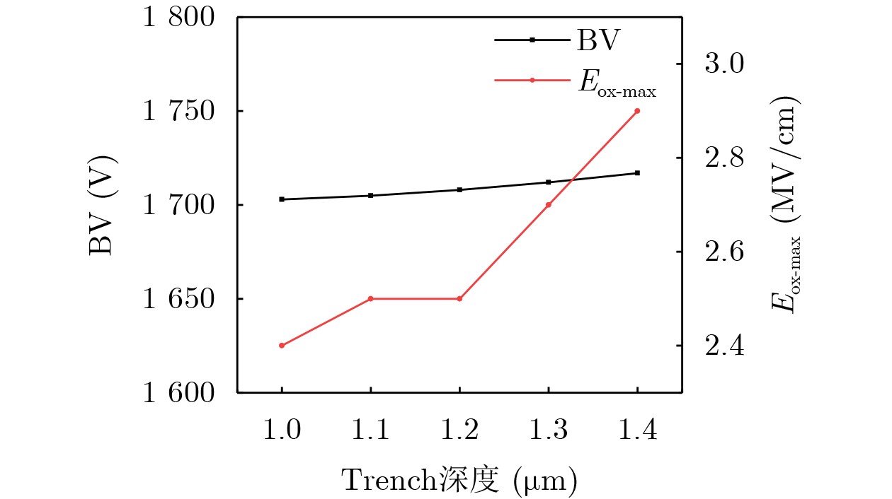
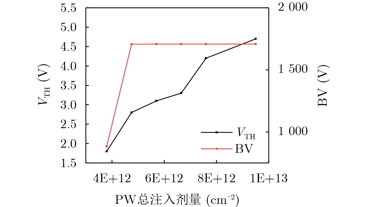
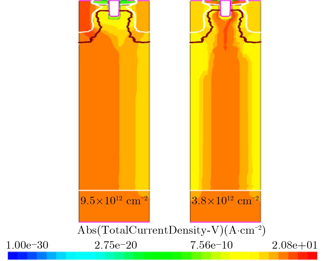
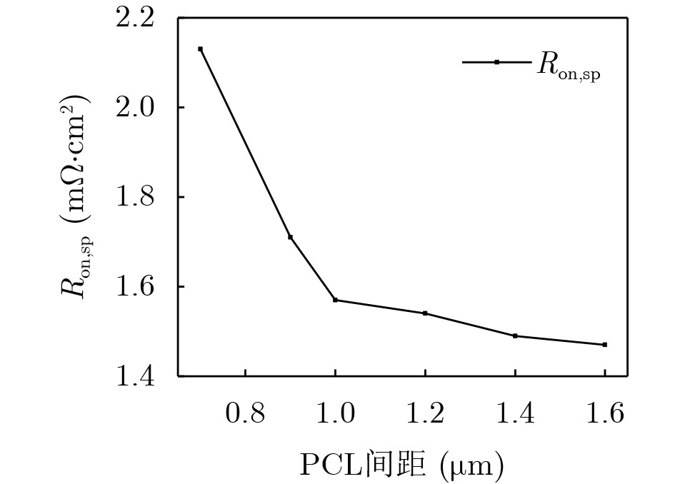
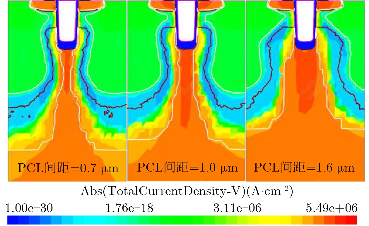
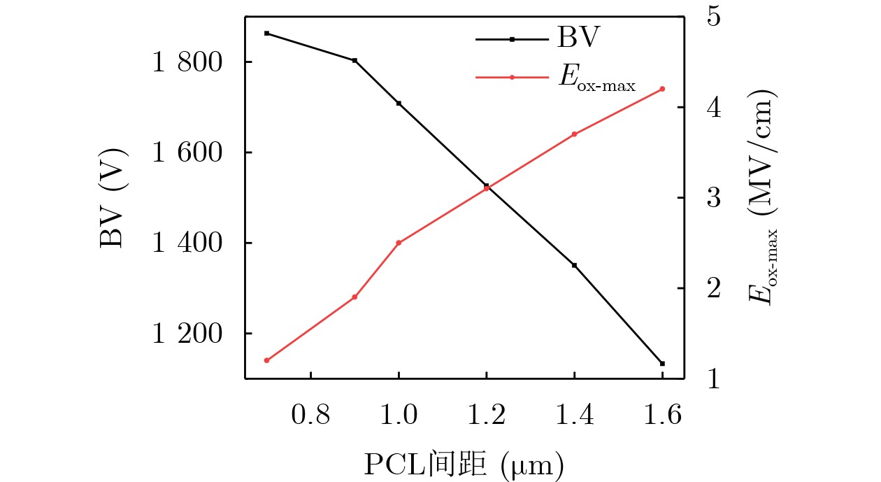
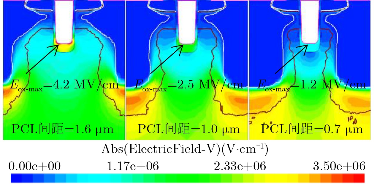
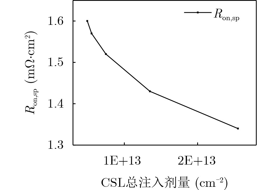
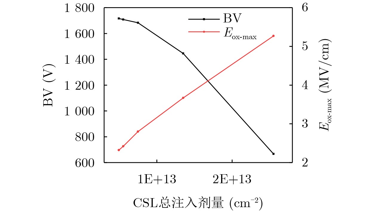
1200 V等级沟槽型SiC MOSFET的结构设计与电学特性仿真研究。通过双侧P型柱(PCL)与电流扩展层(CSL)协同设计,有效优化了器件在阻断状态下的电场分布与导通状态下的电流输运性能。系统仿真分析了外延层掺杂浓度(NEpi)、沟槽宽度与深度、P型阱区(PW)注入剂量、PCL间距及CSL注入剂量等关键结构参数对器件比导通电阻(Ron,sp)、阈值电压(VTH)、击穿电压(BV)及栅氧峰值电场(Eox-max)的影响机制。研究结果表明,优化后的器件可实现VTH=4.7 V, Ron,sp=1.57 mΩ·cm2, BV=1708 V, Eox-max=2.5 MV/cm的良好性能折衷。该研究为开发高性能沟槽型SiC MOSFET提供了系统的仿真方法与设计依据。Abstract:Objective 1 200 V Silicon Carbide (SiC) trench Metal-Oxide-Semiconductor Field-Effect Transistors (MOSFETs) are key devices in medium- and high-voltage power conversion systems. They feature high switching performance, low conduction loss, and high-temperature stability. However, conventional trench structures suffer from electric-field concentration at the trench corner and bottom gate oxide. This effect can cause the peak gate oxide electric field to exceed the industrial reliability criterion of 3 MV/cm, reducing long-term reliability. In addition, strong trade-offs exist among breakdown voltage, specific on-resistance, threshold voltage, and peak gate oxide electric field. These trade-offs make it difficult to achieve high efficiency and high reliability at the same time. To address these issues, this work studies a synergistic structure that combines deep P-type Column (PCL), Carrier Storage Layer (CSL), and locally thickened gate oxide. The aim is to regulate the electric-field distribution, suppress electric-field concentration, improve carrier transport, and achieve balanced device performance. This study provides a systematic design method for high-reliability and high-performance 1 200 V Trench SiC MOSFETs for industrial applications. Methods Numerical device simulations were performed using a Technology Computer-Aided Design (TCAD) platform to analyze and optimize the electrical performance of 1 200 V Trench SiC MOSFETs. To ensure reliable simulations, physical models were used for bandgap narrowing, Shockley-Read-Hall (SRH) recombination, Auger recombination, avalanche breakdown, incomplete dopant ionization, doping- and temperature-dependent mobility, and high-field mobility saturation. A device structure with deep PCL, CSL, and locally thickened bottom gate oxide is constructed to reduce the peak gate oxide electric field and improve device reliability. Key structural and process parameters were swept and quantitatively analyzed. These parameters included epitaxial layer thickness (TEpi), epitaxial layer doping concentration (NEpi), trench width, trench depth, P-Well (PW) implantation dose, PCL spacing, and CSL implantation dose. Static electrical characteristics, including threshold voltage (Vth), specific on-resistance (Ron,sp), Breakdown Voltage (BV), and peak gate oxide electric field (Eox,max) are extracted and evaluated. The final parameter combination is finally determined through a trade-off analysis between conduction performance and long-term device reliability. Results and Discussions The simulation results show that the deep PCL structure redirects electric-field lines away from the trench bottom gate oxide and reduces electric-field concentration. When this structure is combined with the locally thickened bottom gate oxide, Eox-max is reduced below 3 MV/cm, meeting the industrial reliability criterion. The CSL broadens the vertical conduction path, reduces current crowding, and decreases Ron,sp. Parameter optimization shows that TEpi, NEpi, trench dimensions, PW implantation dose, and CSL implantation dose determine the trade-off between BV and conduction performance ( Fig. 5 ,Fig. 6 ,Fig. 9 ,Fig. 10 , andFig. 19 ). PCL spacing has a strong effect on electric-field shielding and gate oxide protection (Fig. 16 andFig. 17 ). After multi-parameter optimization, the device achieves VTH=4.7 V, BV=1 708 V, Ron,sp=1.57 mΩ·cm2, and Eox-max=2.5 MV/cm (Table 2 ). These results indicate balanced performance for high-voltage power applications.Conclusions A synergistic PCL-CSL structural design for 1 200 V Trench SiC MOSFETs is studied and validated through TCAD simulation. The design addresses key limitations of conventional Trench SiC MOSFETs, including high peak gate oxide electric field, limited breakdown capability, and the trade-off between conduction performance and reliability. The effects of TEpi, NEpi, trench dimensions, PW implantation dose, PCL spacing, and CSL implantation dose on device performance and gate oxide reliability are clarified through parameter sweeping and comparative analysis. With coordinated structural optimization, the optimized device achieves low Ron,sp, high BV, suitable VTH, and suppressed electric-field concentration near the trench bottom oxide. Eox-max is controlled below the 3 MV/cm industrial reliability criterion, which reduces the risk of oxide degradation under high-bias operation. The proposed structural strategy and optimization method provide guidance for the design, simulation, and process development of high-voltage, high-reliability SiC power devices. -
表 1 沟槽型SiC MOSFET的主要结构参数以及性能参数
参数 数值 Cell宽度 2.8 μm EPI深度 12 μm EPI浓度 1×1016 cm–3 PCL掺杂 总剂量5×1014 cm–2,5步注入 PW掺杂 总剂量9.5×1012 cm–2,4步注入 CSL掺杂 总剂量5×1012 cm–2,5步注入 PW结深 0.7 μm Trench宽度 0.7 μm Trench深度 1.2 μm 侧壁氧化层厚度 50 nm 底部氧化层厚度 200 nm VTH 5.0 V Ron,sp 1.70 mΩ·cm2 BV 1712 VEox-max 2.6 MV/cm  下载: 导出CSV
表 2 器件关键结构参数以及主要性能参数
参数 数值 Cell宽度 2.8 μm EPI深度 12 μm EPI浓度 1×1016 cm–3 PCL掺杂 总剂量5×1014 cm–2,5步注入 PCL间距 1.0 μm PW掺杂 总剂量9.5×1012 cm–2,4步注入 CSL掺杂 总剂量5×1012 cm–2,5步注入 PW结深 0.7 μm Trench宽度 0.5 μm Trench深度 1.1 μm 侧壁氧化层厚度 50 nm 底部氧化层厚度 200 nm VTH 4.7 V Ron,sp 1.57 mΩ·cm2 BV 1708 VEox-max 2.5 MV/cm
下载: 导出CSV
-
[1] YUAN Xibo, LAIRD I, and WALDER S. Opportunities, challenges, and potential solutions in the application of fast-switching SiC power devices and converters[J]. IEEE Transactions on Power Electronics, 2021, 36(4): 3925–3945. doi: 10.1109/TPEL.2020.3024862. [2] ZHANG Lei, YUAN Xibo, WU Xiaojie, et al. Performance evaluation of high-power SiC MOSFET modules in comparison to Si IGBT modules[J]. IEEE Transactions on Power Electronics, 2019, 34(2): 1181–1196. doi: 10.1109/TPEL.2018.2834345. [3] ZHANG Xuan, YAO Chengcheng, LI Cong, et al. A wide bandgap device-based isolated quasi-switched-capacitor DC/DC converter[J]. IEEE Transactions on Power Electronics, 2014, 29(5): 2500–2510. doi: 10.1109/TPEL.2013.2287501. [4] TEGA N, HISAMOTO D, SHIMA A, et al. Channel properties of SiC trench-etched double-implanted MOS (TED MOS)[J]. IEEE Transactions on Electron Devices, 2016, 63(9): 3439–3444. doi: 10.1109/TED.2016.2587799. [5] YANG Tongtong, WANG Yan, and YUE Ruifeng. SiC trench MOSFET with reduced switching loss and increased short-circuit capability[J]. IEEE Transactions on Electron Devices, 2020, 67(9): 3685–3690. doi: 10.1109/TED.2020.3005992. [6] TEGA N, YOSHIMOTO H, HISAMATO D, et al. Novel trench-etched double-diffused SiC MOS (TED MOS) for overcoming tradeoff between RonA and Qgd[C]. 2015 IEEE 27th International Symposium on Power Semiconductor Devices & IC’s, Hong Kong, China, 2015: 81–84. doi: 10.1109/ISPSD.2015.7123394. [7] WILLIAMS R K, DARWISH M N, BLANCHARD R A, et al. The trench power MOSFET: Part I—history, technology, and prospects[J]. IEEE Transactions on Electron Devices, 2017, 64(3): 674–691. doi: 10.1109/TED.2017.2653239. [8] YU Hengyu, LIANG Shiwei, LIU Hangzhi, et al. Numerical study of SiC MOSFET with integrated n-/n-type poly-Si/SiC heterojunction freewheeling diode[J]. IEEE Transactions on Electron Devices, 2021, 68(9): 4571–4576. doi: 10.1109/TED.2021.3097979. [9] KONG Lingxu, CHEN Sizhe, REN Na, et al. High-performance 10-kV-rated, 175-mΩ 4H-SiC MOSFETs with MeV JFET implantation and efficient termination[J]. IEEE Transactions on Electron Devices, 2025, 72(8): 4246–4253. doi: 10.1109/TED.2025.3574110. [10] GUO Jingwei, LI Ping, JIANG Jie, et al. A new 4H-SiC Trench MOSFET with improved reverse conduction, breakdown, and switching characteristics[J]. IEEE Transactions on Electron Devices, 2023, 70(1): 172–177. doi: 10.1109/TED.2022.3225121. [11] LIU Yong, FENG Hao, PENG Xin, et al. Experimental demonstration of the double-trench, buried-P JTE edge termination with short edge width and high dV/dt capability for 1200 V-class SiC devices[C]. 2024 36th International Symposium on Power Semiconductor Devices and ICs, Bremen, Germany, 2024: 17–20. doi: 10.1109/ISPSD59661.2024.10579614. [12] YUAN Jun, CHEN Wei, GUO Fei, et al. Design and fabrication of a novel 1200 V 4H-SiC trench MOSFET with periodically grounded trench bottom shielding[J]. IEEE Transactions on Electron Devices, 2025, 72(6): 3063–3067. doi: 10.1109/TED.2025.3559888. [13] KIM D, JANG S Y, MORGAN A J, et al. Influence of P+ body on performance and ruggedness of 1.2 kV 4H-SiC MOSFETs[J]. IEEE Transactions on Electron Devices, 2024, 71(12): 7659–7665. doi: 10.1109/TED.2024.3474615. [14] LYNCH J, MANCINI S, DEBOER S, et al. A novel 6.5 kV 4H-SiC MOSFET with a one-channel layout[C]. 2024 36th International Symposium on Power Semiconductor Devices and ICs, Bremen, Germany, 2024: 124–127. doi: 10.1109/ISPSD59661.2024.10579673. [15] KONG Lingxu, CHEN Sizhe, REN Na, et al. 1 cm2 Chip Size, 10 kV Rated 4H-SiC MOSFETs with efficient termination design and state-of-the-art device performance[C]. 2025 37th International Symposium on Power Semiconductor Devices and ICs, Kumamoto, Japan, 2025: 381–384. doi: 10.23919/ISPSD62843.2025.11117312. [16] PETERS D, SIEMIENIEC R, AICHINGER T, et al. Performance and ruggedness of 1200V SiC—trench—MOSFET[C]. 2017 29th International Symposium on Power Semiconductor Devices and ICs, Sapporo, Japan, 2017: 239–242. doi: 10.23919/ISPSD.2017.7988904. [17] NAKAMURA T, NAKANO Y, AKETA M, et al. High performance SiC trench devices with ultra-low ron[C]. 2011 International Electron Devices Meeting, Washington, USA, 2011: 26.5. 1–26.5. 3. doi: 10.1109/IEDM.2011.6131619. [18] SCHWAIGER S, HEYERS K, MARTINEZ-LIMIA A, et al. Advanced SiC trench-MOS technology for automotive application[C]. PCIM Europe 2023; International Exhibition and Conference for Power Electronics, Intelligent Motion, Renewable Energy and Energy Management, Nuremberg, Germany, 2023: 1–4. doi: 10.30420/566091096. [19] HARADA S, KATO M, KOJIMA T, et al. Determination of optimum structure of 4H-SiC Trench MOSFET[C]. 2012 24th International Symposium on Power Semiconductor Devices and ICs, Bruges, Belgium, 2012: 253–256. doi: 10.1109/ISPSD.2012.6229071. [20] ZHU Shengnan, SHI Limeng, JIN M, et al. Reliability comparison of commercial planar and trench 4H-SiC power MOSFETs[C]. 2023 IEEE International Reliability Physics Symposium (IRPS), Monterey, USA, 2023: 1–5. doi: 10.1109/IRPS48203.2023.10117998. -

 下载:
下载:


图(19) / 表(2)
计量
- 文章访问数: 301
- HTML全文浏览量: 252
- PDF下载量: 14
- 被引次数: 0
