




FPGA Hybrid Programmable Logic Block Architecture for Highly Efficient Resource Utilization
-
摘要: 商用现场可编程门阵列(FPGA)普遍采用6输入查找表(LUT)构建可编程逻辑块,而相关实验表明6输入LUT在电路中的应用平均不超过30%,造成了严重的可编程资源浪费。该文在可拆分因子概念基础上将6输入LUT进行不同粒度拆分并进行重新组合,构建出3种新的混合粒度可编程逻辑单元;然后基于混合粒度可编程逻辑单元组合成3种新的混合可编程逻辑块结构用以替换Xilinx的可编程逻辑块;同时提出了一种对映射后网表进行统计的优化评估算法;最后对3种改进结构进行相应实验验证和评估。结果表明:在不增加输入端口资源的情况下,3种混合粒度可编程逻辑块对Xilinx可编程逻辑块结构替换后面积优化平均超过30%;综合PLB使用数量和面积优化来看,可拆分因子N=3时候构建的混合可编程逻辑块结构优化效果最好,在MCNC电路集和VTR电路集下,资源利用率平均分别提高了8.27%和27.64%,有效提升了FPGA的资源利用率。Abstract:
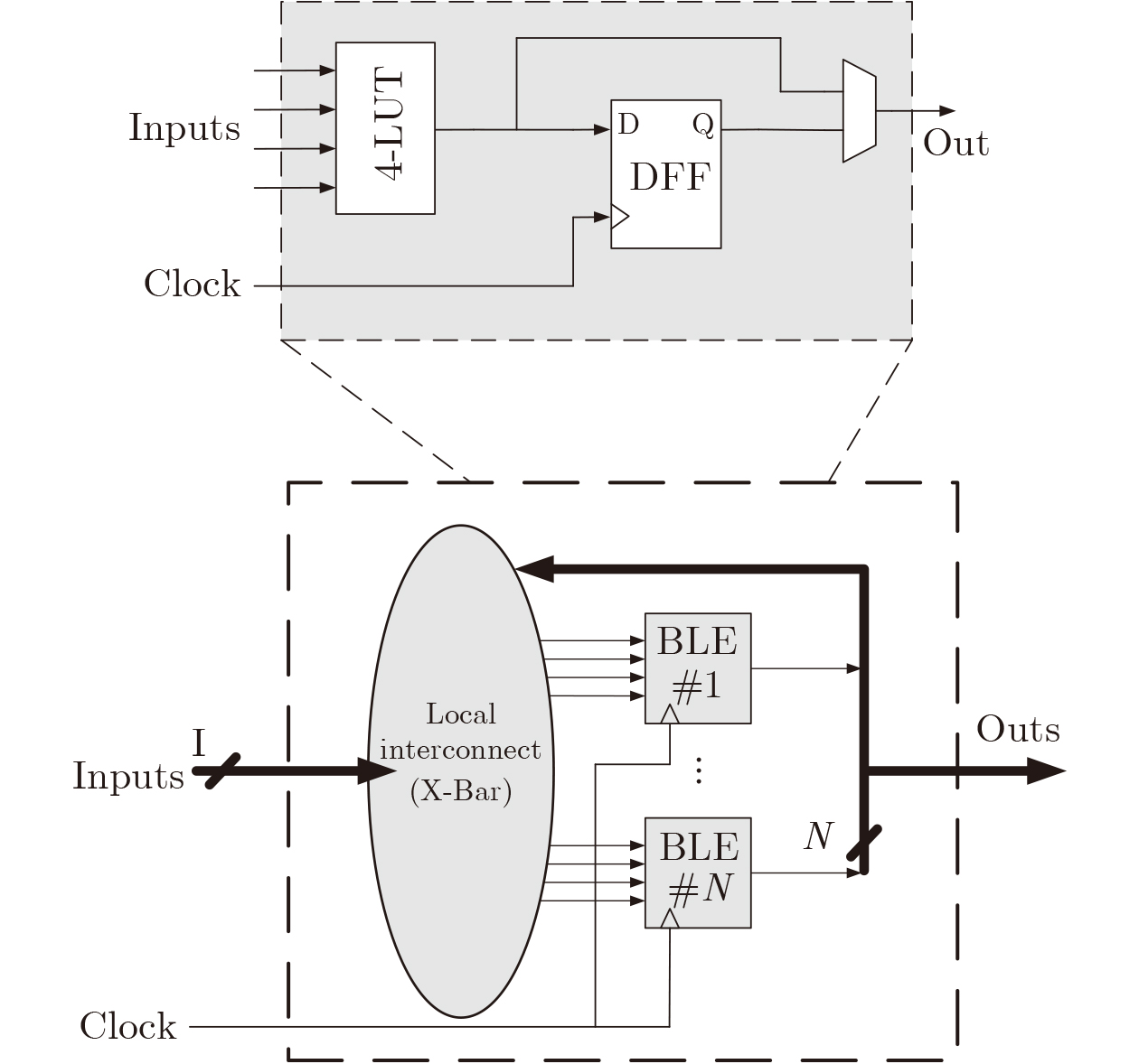
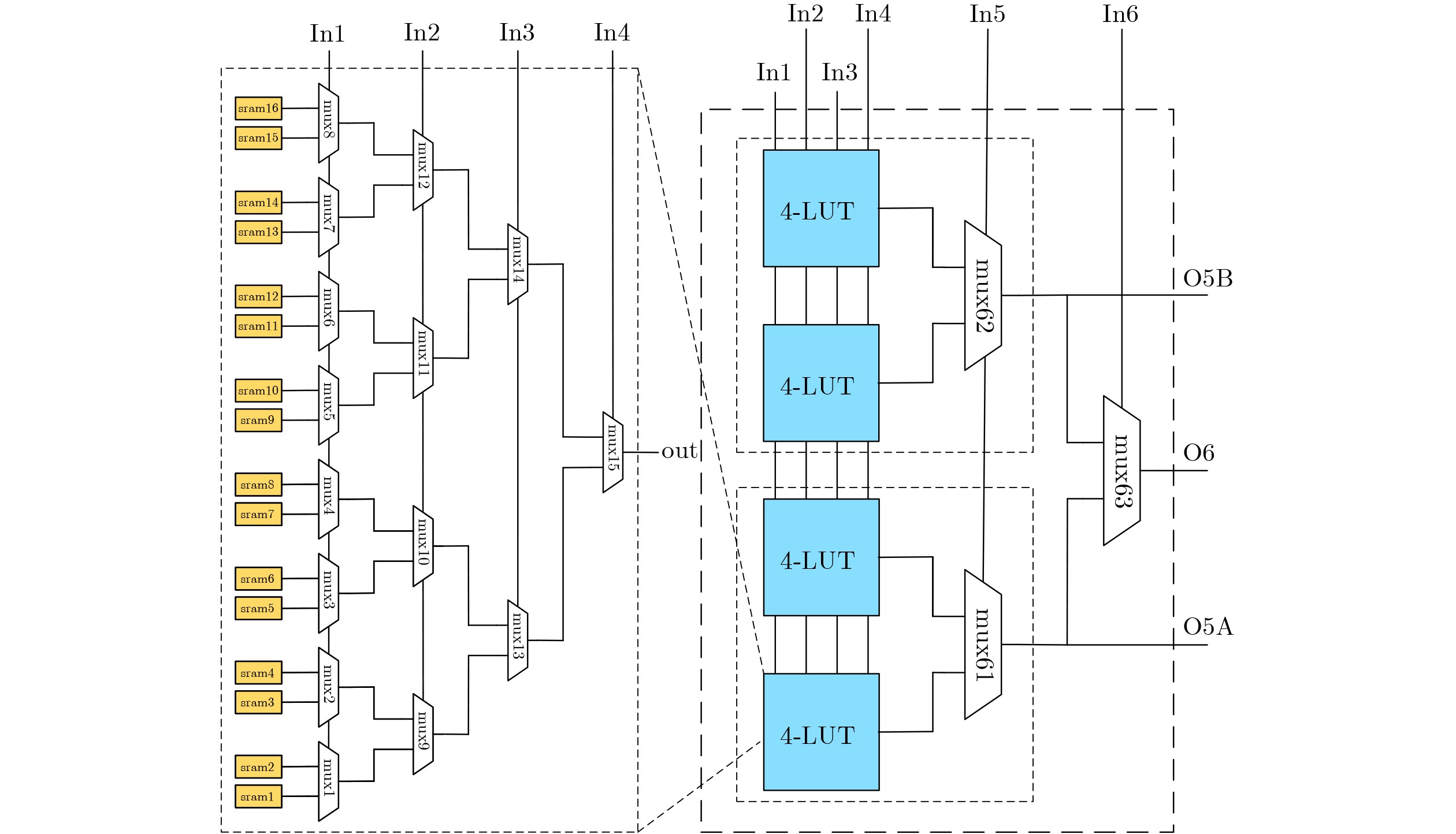
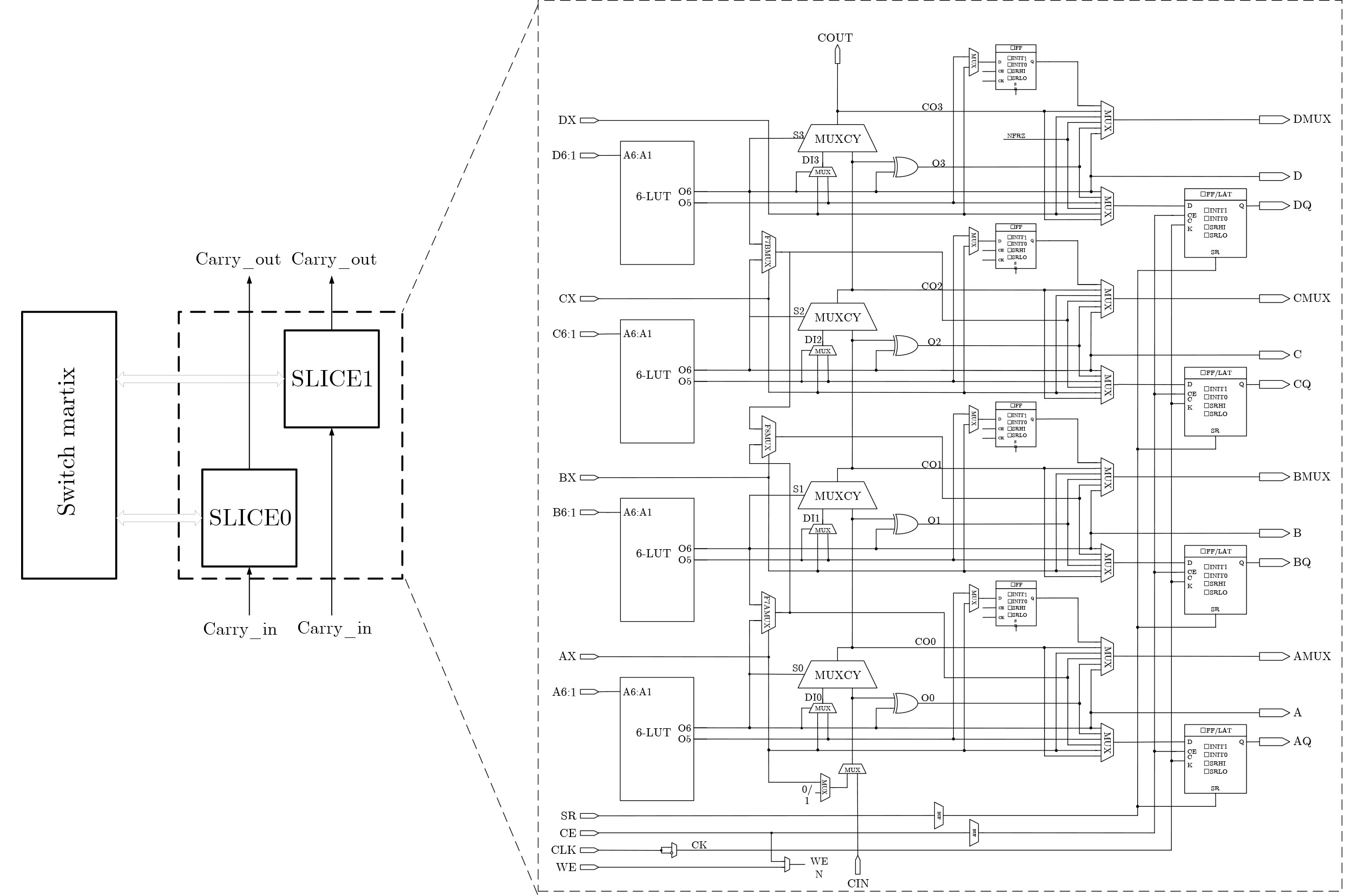
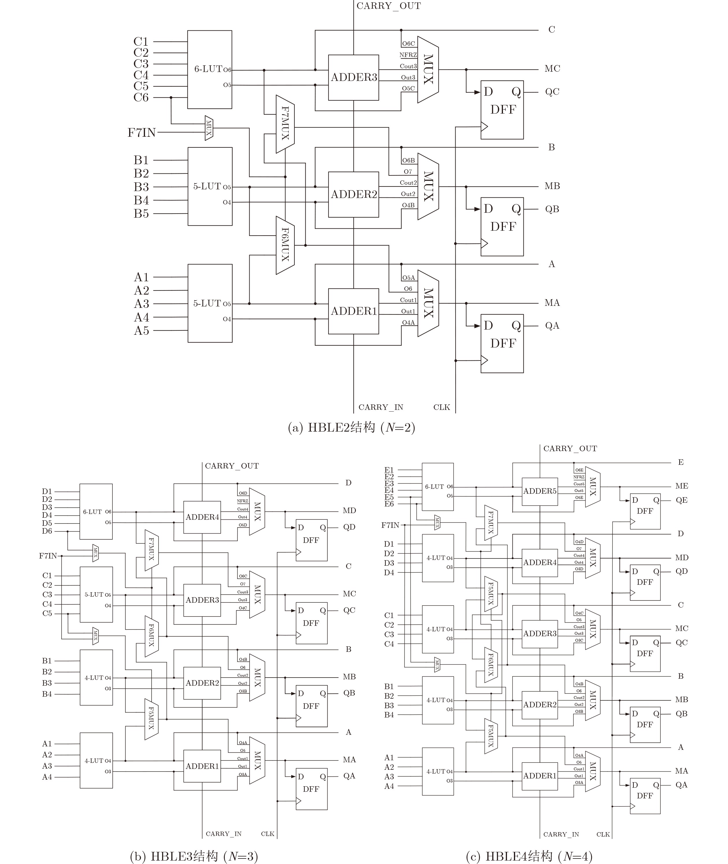
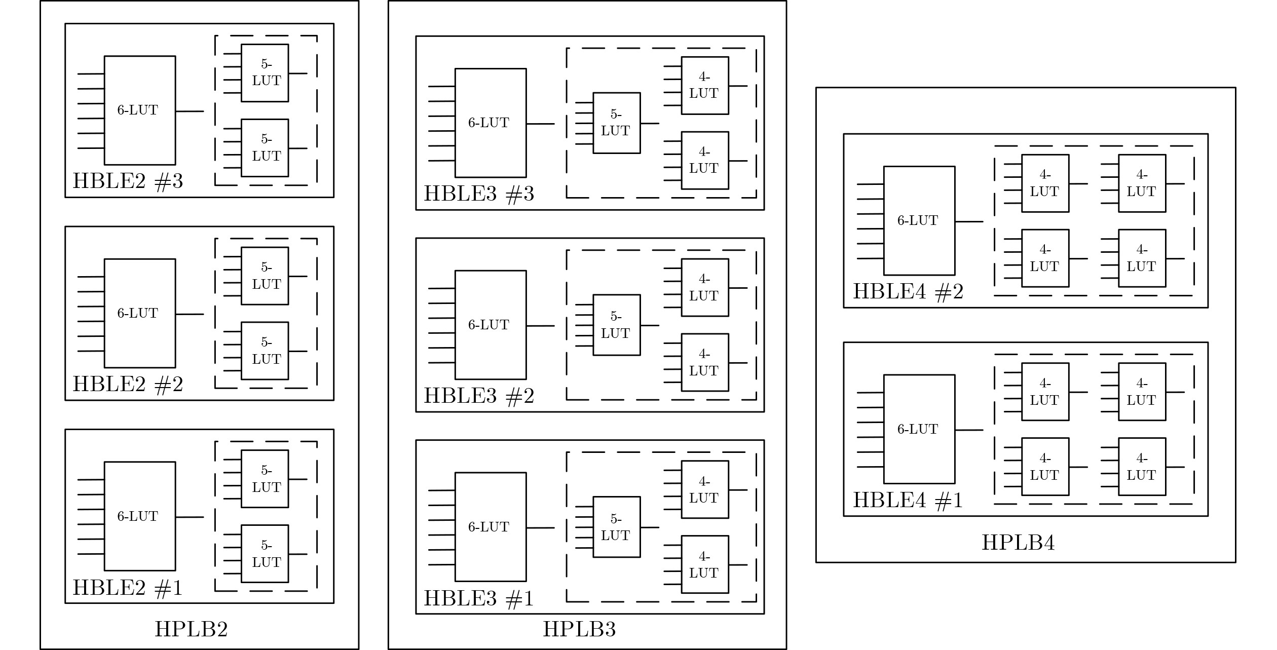
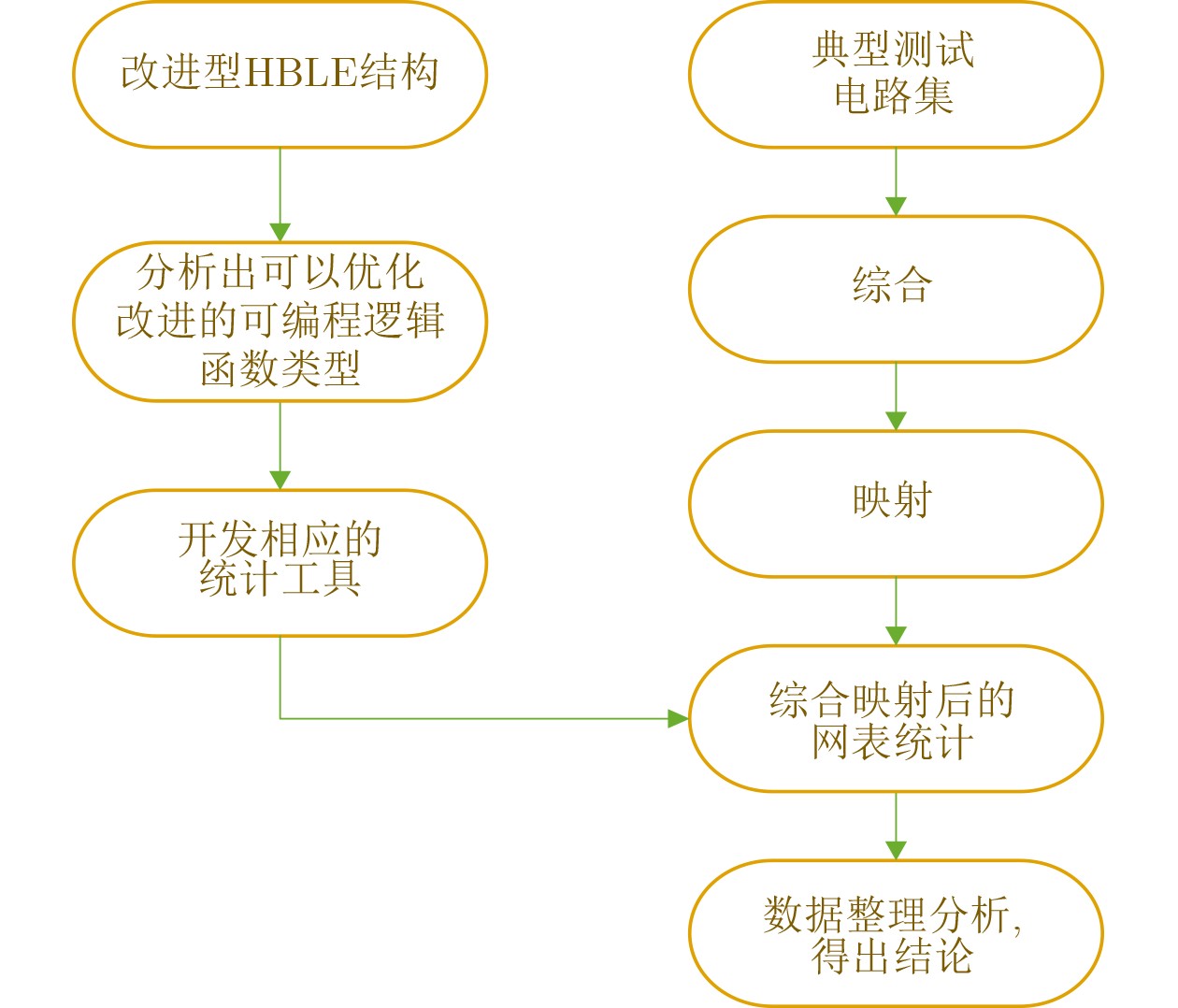
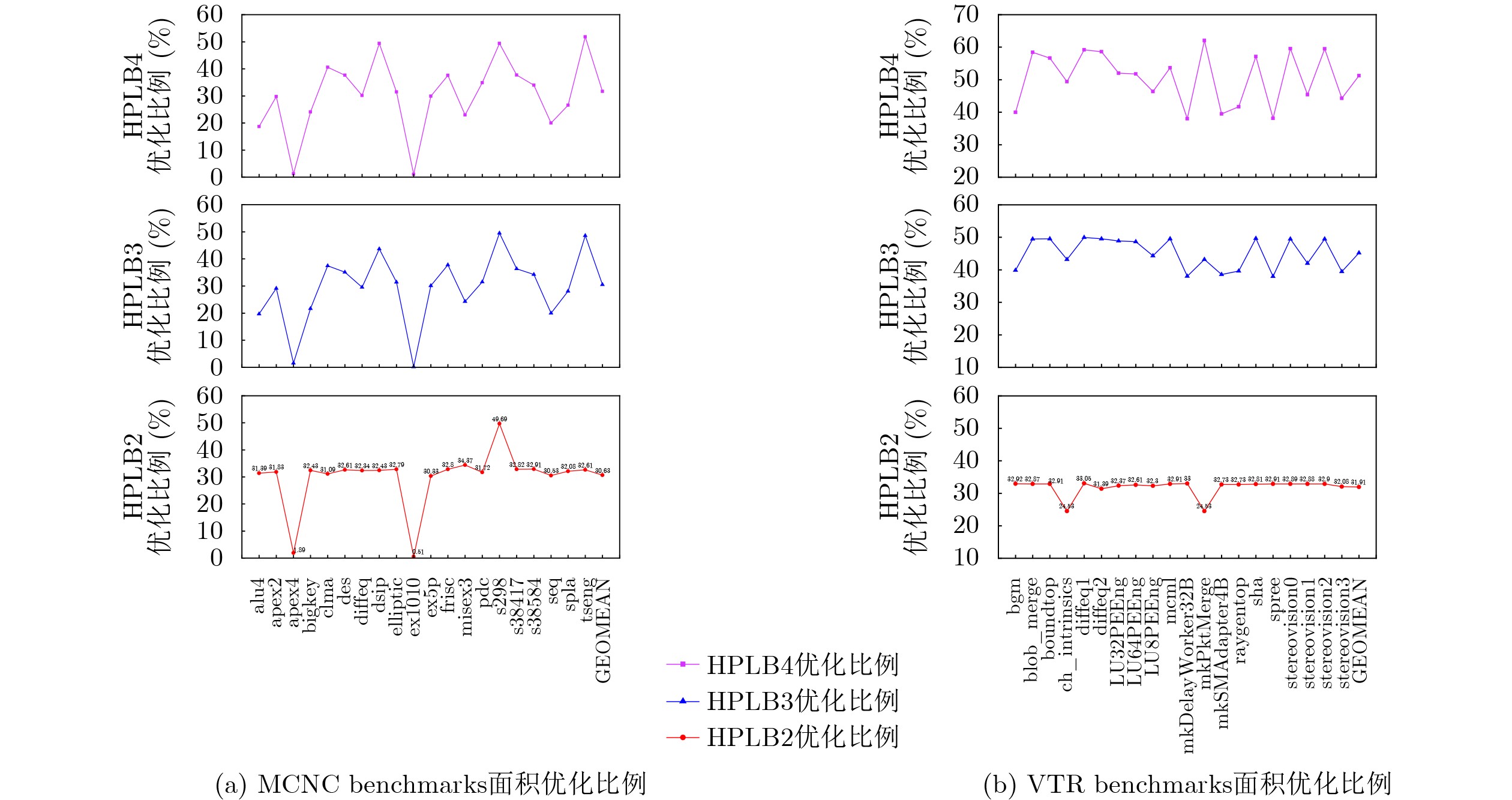
Six-input Look-Up Tables (6-LUTs) are widely used in commercial Field-Programmable Gate Arrays (FPGAs) to construct programmable logic blocks. However, related experiments show that their average utilization in circuits is less than 30%, which leads to substantial waste of programmable resources. In this paper, 6-LUTs are fractured according to fracturable factors and then recombined at different granularities to construct several new Hybrid Basic Logic Elements (HBLEs). Based on these HBLEs, several novel Hybrid Programmable Logic Block (HPLB) architectures are proposed. The programmable logic blocks in Xilinx devices are then replaced with these HPLB architectures. Concurrently, a statistical evaluation algorithm for the mapped netlist is proposed. Finally, several HPLB architectures are experimentally verified and evaluated. Experimental results for the three enhanced architectures show that the HPLBs achieve an average area reduction of more than 30% compared with Xilinx PLBs, without increasing the number of input ports. Among them, the hybrid HPLB architecture with a fracturable factor of N = 3 achieves the best overall optimization when both HPLB utilization and area reduction are considered. Based on the MCNC and VTR benchmarks, the proposed architecture results in average HPLB count increases of 8.27% and 27.64%, respectively, while improving programmable resource utilization. Objective Currently, modern commercial Field-Programmable Gate Array (FPGA) architectures use Six-input Look-Up Tables (6-LUTs) as the fundamental building blocks of basic logic elements. Experimental results show that when circuits are mapped to 6-LUT-based basic logic elements, only about 30% of the logic elements are ultimately implemented as 6-LUTs. When 6-LUTs are used to implement functions with fewer than six inputs, more than half of the logic resources are wasted. This leads to substantial underutilization of programmable resources. Experimental data show that a circuit design mapped to 100 4-LUTs can be fractured into 78 6-LUTs during 6-LUT mapping, with a {6,5,4,3,2}-LUT function distribution of {23,32,17,9,13}. These results indicate that only about 25% of the 6-LUTs are assigned to 6-input functions, whereas the remaining 6-LUTs are underutilized. This further demonstrates the inefficiency of technology mapping for LUTs with a large input size K. Methods The fracturable factor N, defined as the number of sub-LUTs that can be obtained from a single LUT, characterizes the fracturable and reconfigurable nature of LUT architectures in FPGAs. To address the low resource utilization described above, a 6-LUT is fractured into several granularities according to the fracturable factor. Three novel hybrid-granularity divisible logic structures are then constructed by reconnecting and reconfiguring the resulting sub-LUTs with additional input ports and multiplexer modules. The optimization effects of these three Hybrid Basic Logic Element (HBLE) topologies on FPGA performance are then investigated. The HBLE2 structure consists of one intact 6-LUT and one divisible 6-LUT split into two 5-LUTs with a fracturable factor of N = 2. The HBLE3 structure consists of one intact 6-LUT and one divisible 6-LUT split into one 5-LUT and two 4-LUTs with a fracturable factor of N = 3. The HBLE4 structure consists of one intact 6-LUT and one divisible 6-LUT split into four 4-LUTs with a fracturable factor of N = 4. All three HBLE structures support adder units and allow either latched output or direct combinational logic output. They also support direct latched output without passing through combinational logic. A Hybrid Programmable Logic Block (HPLB) is formed by combining several HBLEs. Two widely used academic benchmark sets, the MCNC circuit set and the VTR circuit set, are selected for experimental evaluation. Each circuit set is mapped onto a Xilinx Virtex-7 FPGA. The mapped netlist is then analyzed to count the types and numbers of LUTs used. After the data are organized with the corresponding greedy algorithms, the minimum number of Configurable Logic Blocks (CLBs) required is determined. Because each Xilinx CLB contains eight 6-LUTs, the greedy algorithm uses the total LUT number fractured by 8 to estimate the minimum number of CLBs required after benchmark mapping. To ensure comparable conditions, each structure is also reorganized with the greedy algorithm after the Xilinx CLB structure is replaced by the HPLB structure proposed in this study. This yields the minimum number of HPLBs required. In practical packing, not every LUT in the mapped CLBs can be used because of routing constraints. Therefore, the optimized result obtained after greedy restructuring represents the theoretical lower bound under ideal optimization conditions. Results and Discussions For the MCNC circuit set, replacing CLB structures with HPLBs reduces the average number of required blocks by about 8% for both the HPLB2 and HPLB3 structures. However, the HPLB4 structure increases the required block count by more than 30% on average. For the VTR circuit set, fewer HPLBs are required than CLBs after replacement. On average, the counts for HPLB2 and HPLB4 decrease by less than 10%, whereas the count for HPLB3 decreases by about 30%. This allows more efficient SRAM scheduling and fuller use of input pins. In contrast, the uniform CLB structure requires more CLBs when functions with a small LUT input size K are implemented because of resource waste. According to the post-mapping HPLB counts, the HPLB4 structure performs less effectively than the HPLB3 structure. Analysis of post-mapping area optimization shows that both the MCNC and VTR circuit sets achieve average area reduction ratios of more than 30%. On the MCNC benchmark set, all three HPLB structures achieve area optimization ratios of about 31%. On the VTR benchmark set, the optimization effects differ: HPLB2 achieves an average area reduction of 30.63%, whereas HPLB4 achieves an average reduction of 51.21%. HPLB3 achieves a 45.22% area reduction, which is slightly lower than that of HPLB4. Detailed analysis of the area optimization results shows that a higher fracturable factor N provides greater benefits for integrating small-scale LUTs in circuits, resulting in larger area reduction ratios in the enhanced architectures. Conclusions To address the low resource utilization of 6-LUTs, this study proposes three HPLB enhancement architectures based on split granularity. These HPLBs replace the Xilinx CLB structure, and an evaluation procedure and matching algorithms are established to examine the advantages of the proposed structures in resource utilization. Evaluation experiments based on the MCNC and VTR benchmark suites show that although HPLB4 achieves substantial area optimization, it also requires more HPLBs, which increases interconnect area. Both HPLB2 and HPLB3 achieve average area reductions of more than 30%. As the scale of the test circuits increases, HPLB3 provides a greater increase in HPLB count and a stronger area optimization effect than HPLB2. Therefore, after the CLB structure is replaced, HPLB3 provides a better balance between HPLB usage and area optimization, and substantially improves the utilization of programmable resources. -
Key words:
- Field programmable gate array /
- Programmable logic block /
- Look-up table /
- Mapping /
- Fracturable factor
-
1 贪心算法优化HPLB2替换Virtex-7 CLB结构后HPLB数量统计
输入:netlist_lut_set:BMs电路映射后网表中统计出来的所有类型LUT对应数量的集合;
lut5_set/lut6_set:netlist_lut中5-LUT/6-LUT的数量;
slut4_set:netlist_lut中K-LUT (K=1,2,3,4)的数量之和;输出:ple:netlist_lut中用贪心算法计算出来的所需的PLE的数目(向上取整); 1: read(netlist_lut_set); 2: stop←max (slut4_set/6,lut5_set/3,lut6_set/3); 3: for ple←1 to stop do 4: x←3lut6_set-ple; 5: if x≥0 then 6: y←3ple–x-lut_set5; 7: if y<0 then 8: z←6ple–2x+2y; 9: result←z-slut4; 10: if result≥0 then 11: write(ple); 12: endif 13: else 14: z←6ple–2x+y; 15: result←z-slut_set4; 16: if result≥0 then 17: write(ple); 18: else 19: y←3ple–x-lut_set5; 20: if y<0 then 21: z←6ple+2y; 22: result←z-lut4_set; 23: if result≥0 then 24: write(ple); 25: endif 26: else 27: z←6ple+y; 28: result←z-slut4_set; 29: if result≥0 then 30: write(ple); 31: endif 32: endif 33: endif 34: endif 35: endif 36: endfor  下载: 导出CSV
表 1 CLB和HPLB结构对MCNC和VTR电路测试集映射后所需PLB数目
MCNC BM #Xilinx CLB #HPLB2 #HPLB3 #HPLB4 VTR BM #Xilinx CLB #HPLB2 #HPLB3 #HPLB4 alu4 33 30 35 53 bgm 1565 1391 1243 1856 apex2 31 28 29 43 blob_merge 778 692 519 639 apex4 20 26 26 39 boundtop 153 136 102 131 bigkey 86 77 89 129 ch_intrinsics 4 4 3 4 clma 23 21 19 27 diffeq1 62 55 41 50 des 56 50 48 69 diffeq2 33 30 22 27 diffeq 58 52 54 80 LU32PEEng 77 69 52 73 dsip 86 77 64 86 LU64PEEng 84 75 57 80 elliptic 201 179 182 272 LU8PEEng 68 61 50 72 ex1010 22 29 29 43 mcml 6599 5866 4399 6036 ex5p 13 12 12 18 mkDelayWorker32B 303 269 248 371 frisc 219 195 180 270 mkPktMerge 4 4 3 3 misex3 23 20 23 35 mkSMAdapter4B 138 123 112 165 pdc 21 19 19 27 raygentop 138 123 110 159 s298 3 2 2 3 sha 164 146 109 139 s38417 182 162 153 224 spree 72 64 59 88 s38584 243 216 211 317 stereovision0 397 353 265 317 seq 88 81 93 139 stereovision1 2070 1841 1585 2232 spla 20 18 19 29 stereovision2 1181 1050 788 945 tseng 84 75 57 80 stereovision3 10 9 8 11 几何平均值 75.6 68.45 67.2 99.15 几何平均值 695 618.05 488.75 669.9 优化比例 - 8.09% 8.27% –34.97% 优化比例 - 9.78% 27.64% 3.62%
下载: 导出CSV
表 2 3种HPLB结构优化效果及结构特点对比你
架构 BMs 平均HPLB数量优化(%) BMs平均面积优化(%) 结构特点 HPLB2 8.94 31.27 ① HPLB2 Tile端口数量与Xilinx CLB接近
② 面积优化比例超过30%
③ HPLB3数量优化比例不到10%HPLB3 18.53 38.32 ① HPLB数量优化效果最好,接近20%
② 面积优化较高,接近40%
③ HPLB3 Tile端口数量最多HPLB4 –14.05 42.26 ① 面积优化效果最好,超过40%
② 每个HPLB中只包含两个HBLE, Tile端口数量最少
③ HPLB数量增加超过10%
下载: 导出CSV
-
[1] BETZ V, ROSE J, and MARQUARDT A. Architecture and CAD for Deep-Submicron FPGAs[M]. New York: Springer, 1999: 127–150. doi: 10.1007/978-1-4615-5145-4. [2] JIANG Xun, WANG Jiarui, MAI Jing, et al. A robust FPGA router with optimization of high-fanout nets and intra-CLB connections[J]. IEEE Transactions on Computer-Aided Design of Integrated Circuits and Systems, 2025, 44(3): 1003–1016. doi: 10.1109/TCAD.2024.3447218. [3] DAHIYA S. Area and delay trade offs in fracturable LUT-based FPGA architectures[J]. Journal of Integrated Science and Technology, 2024, 12(2): 733. [4] KUMARI J L V R, KUMAR V K, ABHIGNYA M, et al. Design and performance analysis of configurable logic block (CLB) for FPGA using various circuit topologies[C]. 2024 3rd International Conference for Innovation in Technology (INOCON), Bangalore, India, 2024: 1–5. doi: 10.1109/INOCON60754.2024.10511683. [5] PUN J, DAI X, ZGHEIB G, et al. Double duty: FPGA architecture to enable concurrent LUT and adder chain usage[J]. IEEE Transactions on Very Large Scale Integration (VLSI) Systems, 2025, 33(2): 412–425. doi: 10.1109/TVLSI.2024.3512345. [6] GUO Yi, ZHOU Qilin, CHEN Xiu, et al. High-efficiency FPGA - based approximate multipliers with LUT sharing and carry switching[C]. 2024 Design, Automation & Test in Europe Conference & Exhibition (DATE), Valencia, Spain, 2024: 1–2. doi: 10.23919/DATE58400.2024.10546667. [7] XIE Yanyue, LI Zhengang, DIACONU D, et al. LUTMUL: Exceed conventional FPGA roofline limit by LUT-based efficient multiplication for neural network inference[C]. Proceedings of the 30th Asia and South Pacific Design Automation Conference, Tokyo, Japan, 2024: 713–719. doi: 10.1145/3658617.3697687. [8] Xilinx Inc. 7 series FPGAs configurable logic block[EB/OL]. https://www.xilinx.com/support/documentation/user_guides/ug474_7Series_CLB.pdf, 2016. [9] HUTTON M, SCHLEICHER J, LEWIS D, et al. Improving FPGA performance and area using an adaptive logic module[C]. Proceedings of the 14th International Conference on Field Programmable Logic and Application, Leuven, Belgium, 2004: 135–144. doi: 10.1007/978-3-540-30117-2_16. [10] 徐宇, 林郁, 江政泓, 等. 拆分粒度对FPGA可拆分逻辑结构性能的影响[J]. 太赫兹科学与电子信息学报, 2017, 15(2): 307–312. doi: 10.11805/TKYDA201702.0307.XU Yu, LIN Yu, JIANG Zhenghong, et al. Influences of fracturable factor on FPGA performance[J]. Journal of Terahertz Science and Electronic Information Technology, 2017, 15(2): 307–312. doi: 10.11805/TKYDA201702.0307. [11] ROSE J, EL GAMAL A, and SANGIOVANNI-VINCENTELLI A. Architecture of field-programmable gate arrays[J]. Proceedings of the IEEE, 1993, 81(7): 1013–1029. doi: 10.1109/5.231340. [12] AHMED E and ROSE J. The effect of LUT and cluster size on deep-submicron FPGA performance and density[J]. IEEE Transactions on Very Large Scale Integration (VLSI) Systems, 2004, 12(3): 288–298. doi: 10.1109/TVLSI.2004.824300. [13] HE Jianshe. Technology mapping and architecture of heterogeneous field-programmable gate arrays[D]. [Master dissertation], University of Toronto, 1993. [14] CONG J and XU Songjie. Delay-optimal technology mapping for FPGAs with heterogeneous LUTs[C]. Proceedings of the 35th Design and Automation Conference, San Francisco, USA, 1998: 704–707. doi: 10.1145/277044.277221. [15] DAHIYA S. Evaluating the impact of cluster parameters on FPGA performance and density[J]. Journal of Integrated Science and Technology, 2023, 11(3): 520. doi: 10.31083/j.jist1130520. [16] SHI Xinyu, YANG Moucheng, LI Zhen, et al. Exploration of FPGA PLB architecture base on LUT and microgates[C]. 2023 International Symposium of Electronics Design Automation (ISEDA), Nanjing, China, 2023: 184–189. doi: 10.1109/ISEDA59274.2023.10218468. [17] SUDHANYA P and JOY VASANTHA RANI S P. Analysis of FPGA architecture with hybrid logic blocks based on ULG and LUT[J]. Journal of Circuits, Systems and Computers, 2025, 34(2): 2550059. doi: 10.1142/S0218126625500598. [18] 高丽江, 杨海钢, 李威, 等. 具有高资源利用率特征的改进型查找表电路结构与优化方法[J]. 电子与信息学报, 2019, 41(10): 2382–2388. doi: 10.11999/JEIT190095.GAO Lijiang, YANG Haigang, LI Wei, et al. A circuit optimization method of improved lookup table for highly efficient resource utilization[J]. Journal of Electronics & Information Technology, 2019, 41(10): 2382–2388. doi: 10.11999/JEIT190095. [19] GARCÍA A. Greedy algorithms: A review and open problems[J]. Journal of Inequalities and Applications, 2025, 2025(1): 11. doi: 10.1186/s13660-025-03254-1. -

 下载:
下载:

图(7) / 表(3)
计量
- 文章访问数: 719
- HTML全文浏览量: 460
- PDF下载量: 39
- 被引次数: 0
