

Research Status and Prospects of Mid-Wavelength Infrared Superlattice Detector Technology
-
摘要: 中波红外探测器具备高灵敏度和优异的温度分辨能力,在国土安全、工业测温、医疗诊断以及遥感监测等民用与军用领域均扮演着至关重要的角色。二类超晶格(T2SL)材料因其能带可调和低俄歇复合率等优势,成为最具潜力的第3代红外探测器材料体系。该文首先阐述量子效率、暗电流密度与比探测率等关键光电参数对探测器性能的影响;随后,聚焦于InAs/GaSb和InAs/InAsSb两大材料体系,系统综述了在暗电流抑制与光响应提升两方面的最新进展,包括势垒结构设计、外延生长优化及器件工艺改进等关键技术,通过这些关键技术研发,探测器性能和工作温度不断提升;最后,对比分析了两类探测器的主要性能指标,并展望了中波超晶格探测技术未来的发展将集中于结构创新设计、大尺寸高质量材料生长、大规模焦平面集成等方面,并有望通过多机制耦合进一步拓展探测性能与应用边界。
-
关键词:
- 二类超晶格 /
- 中波红外 /
- InAs/GaSb /
- InAs/InAsSb
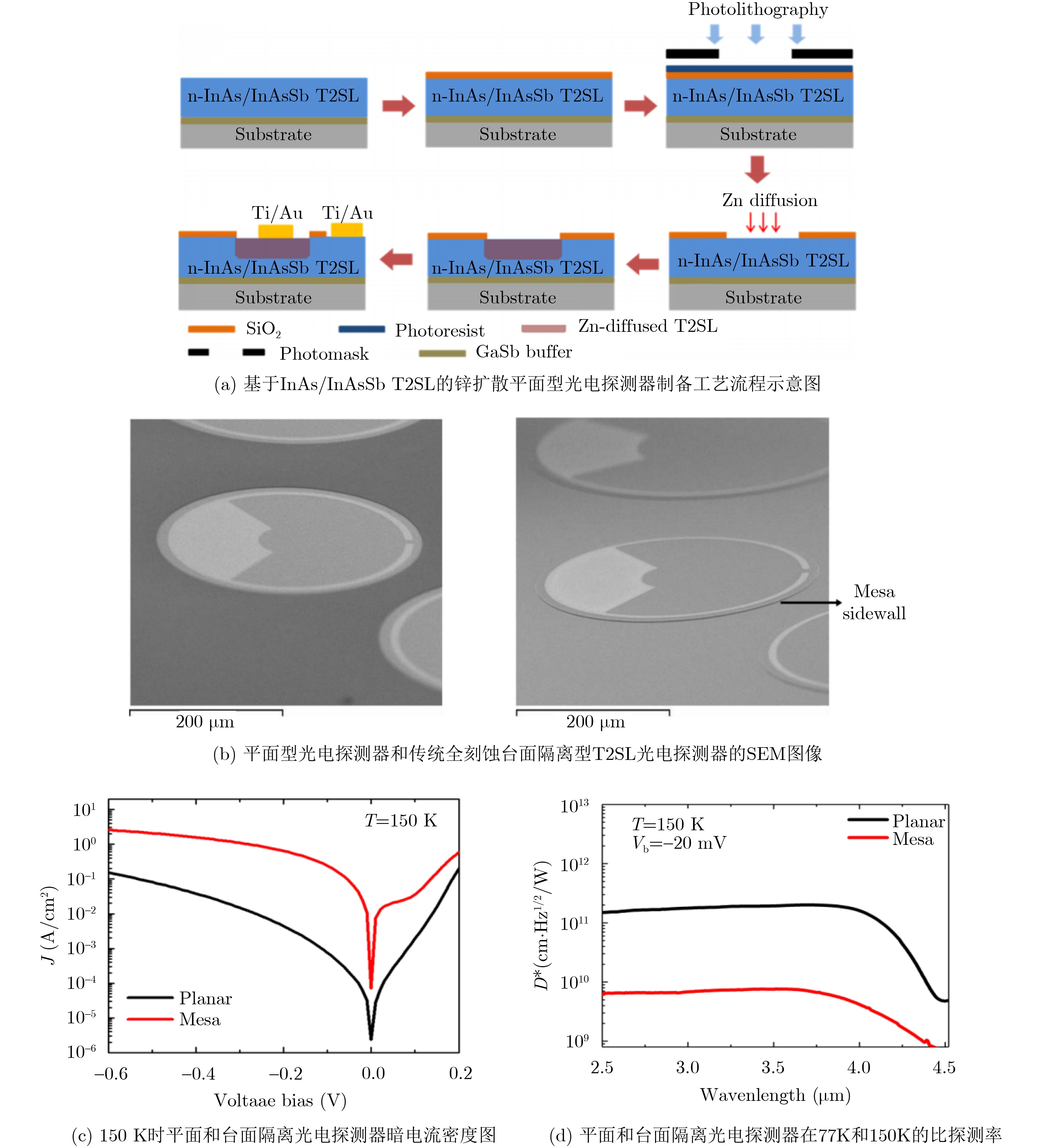
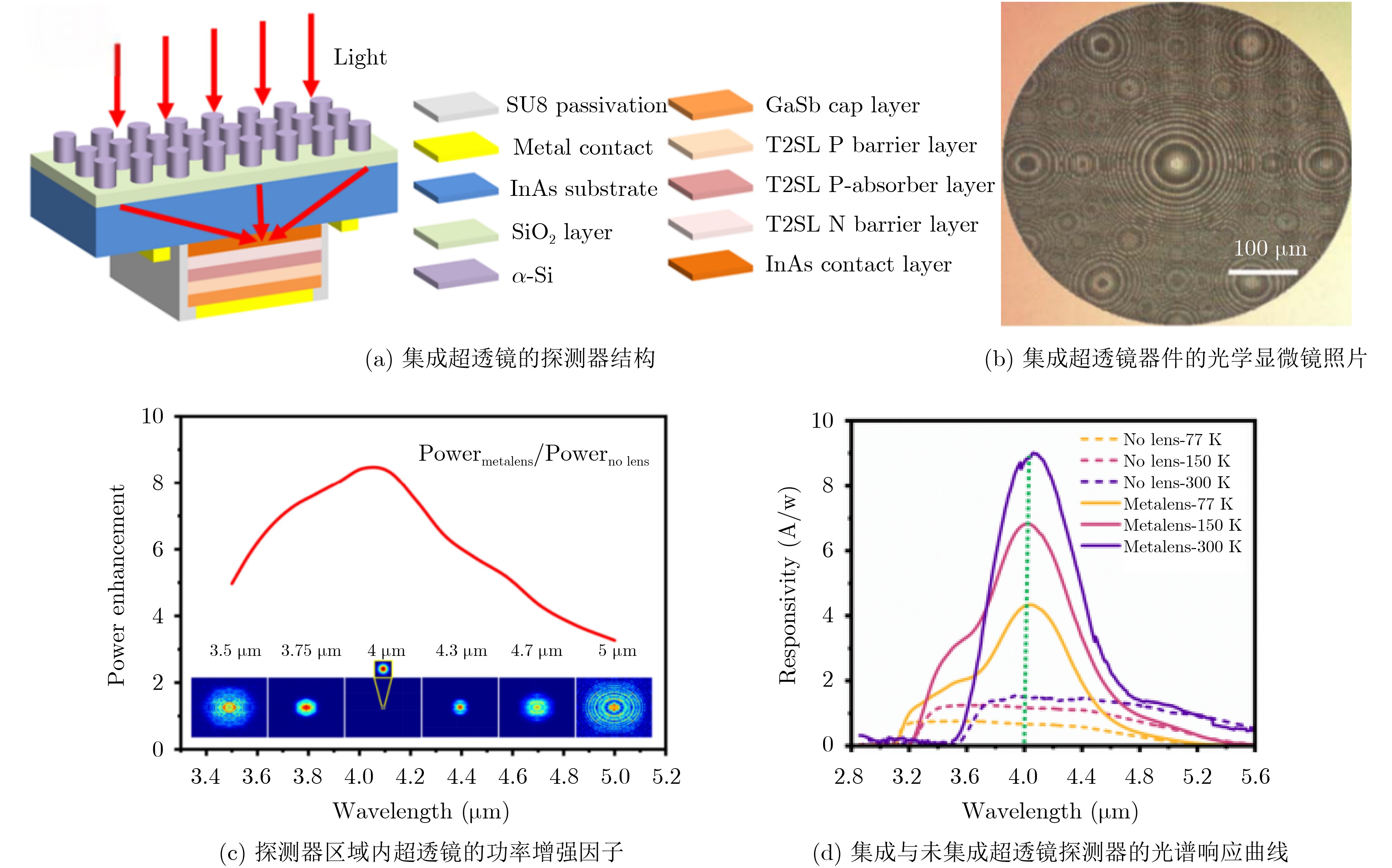
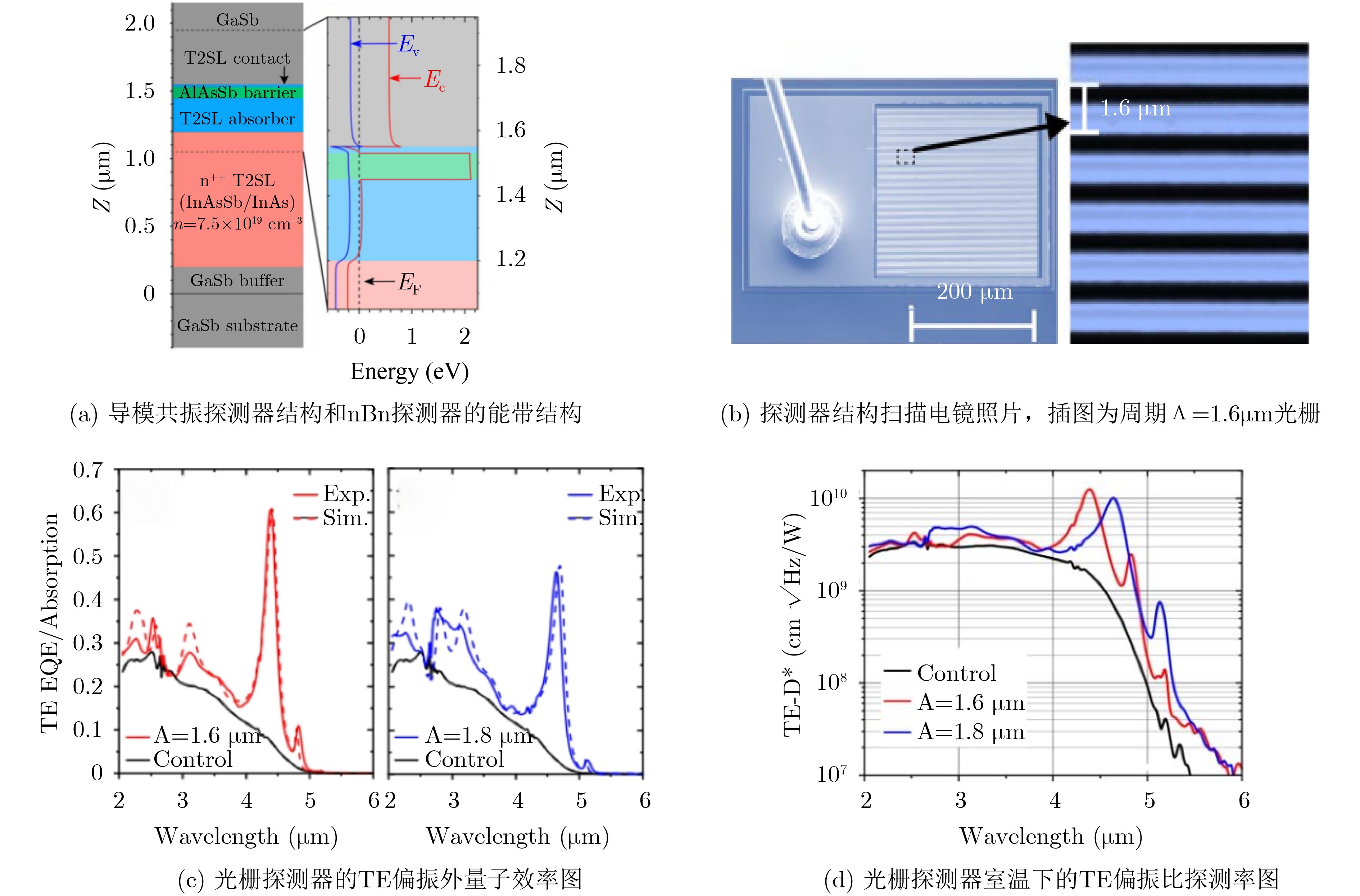
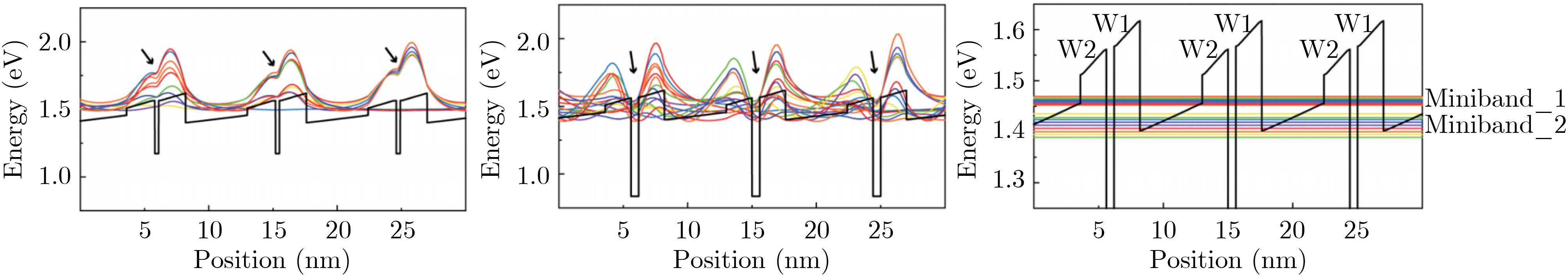
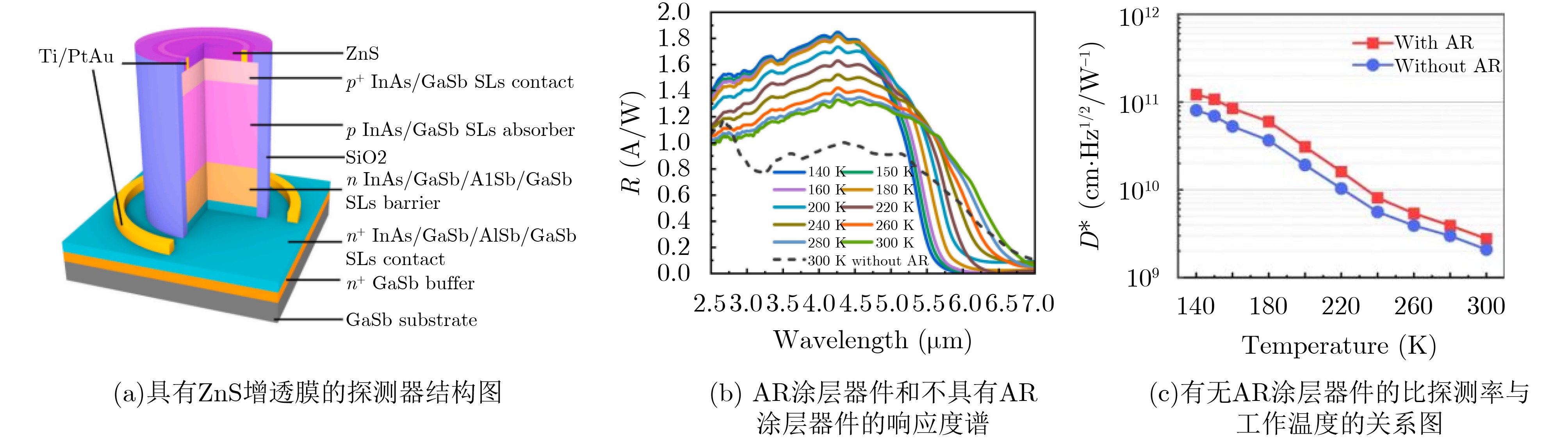
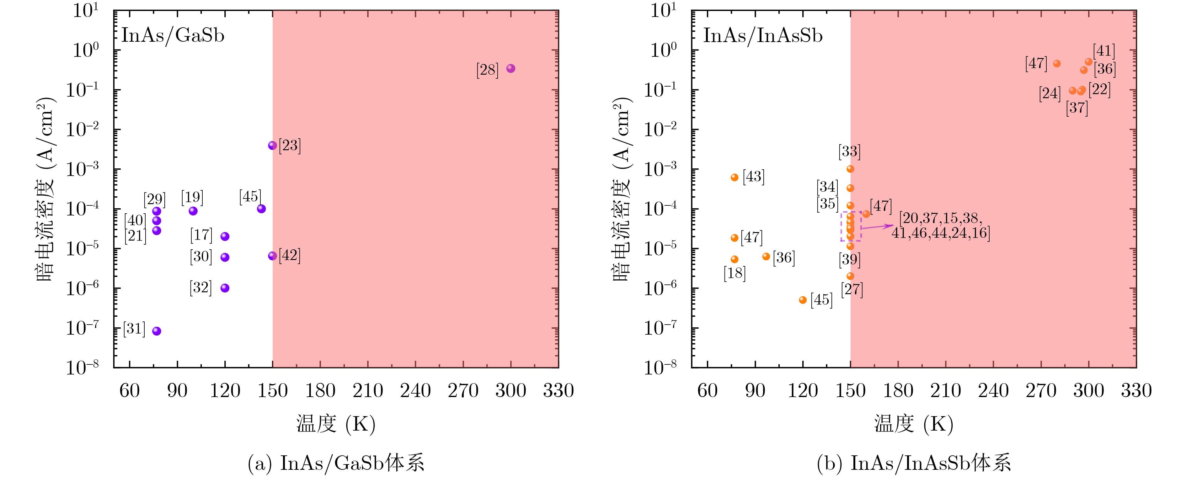
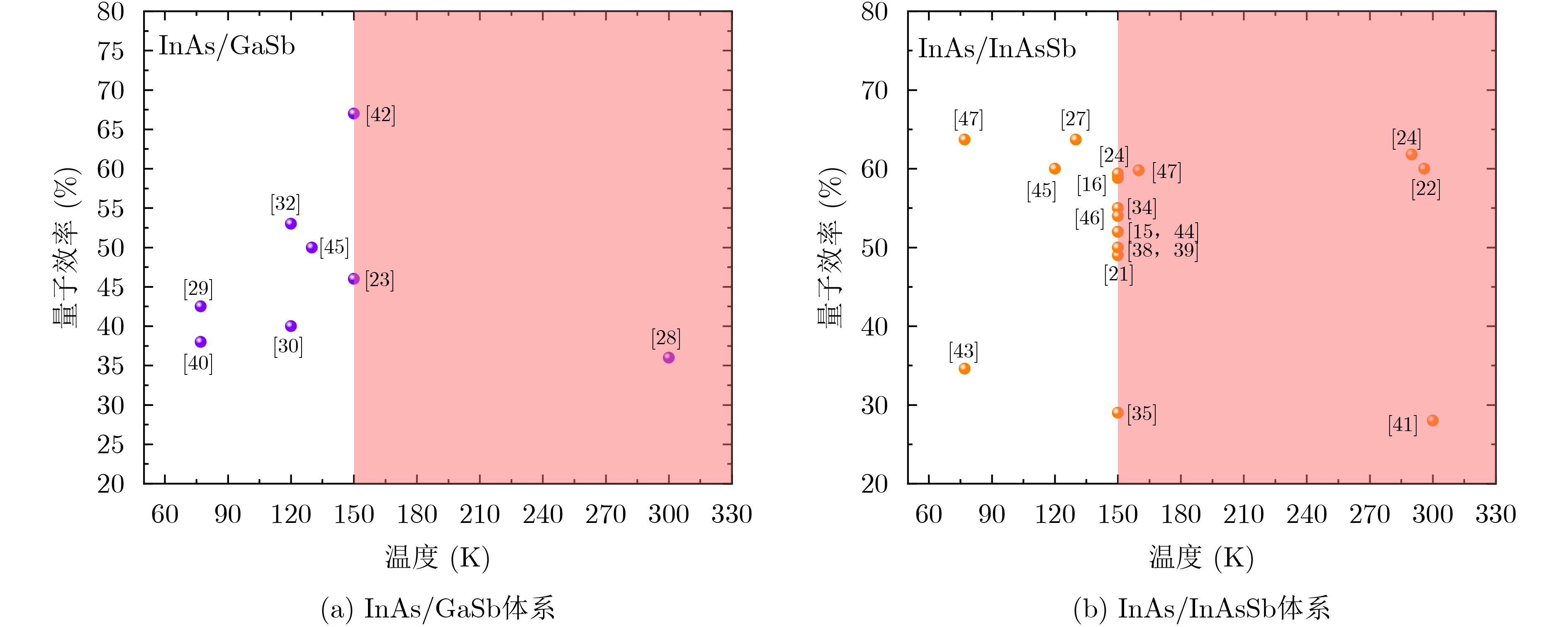
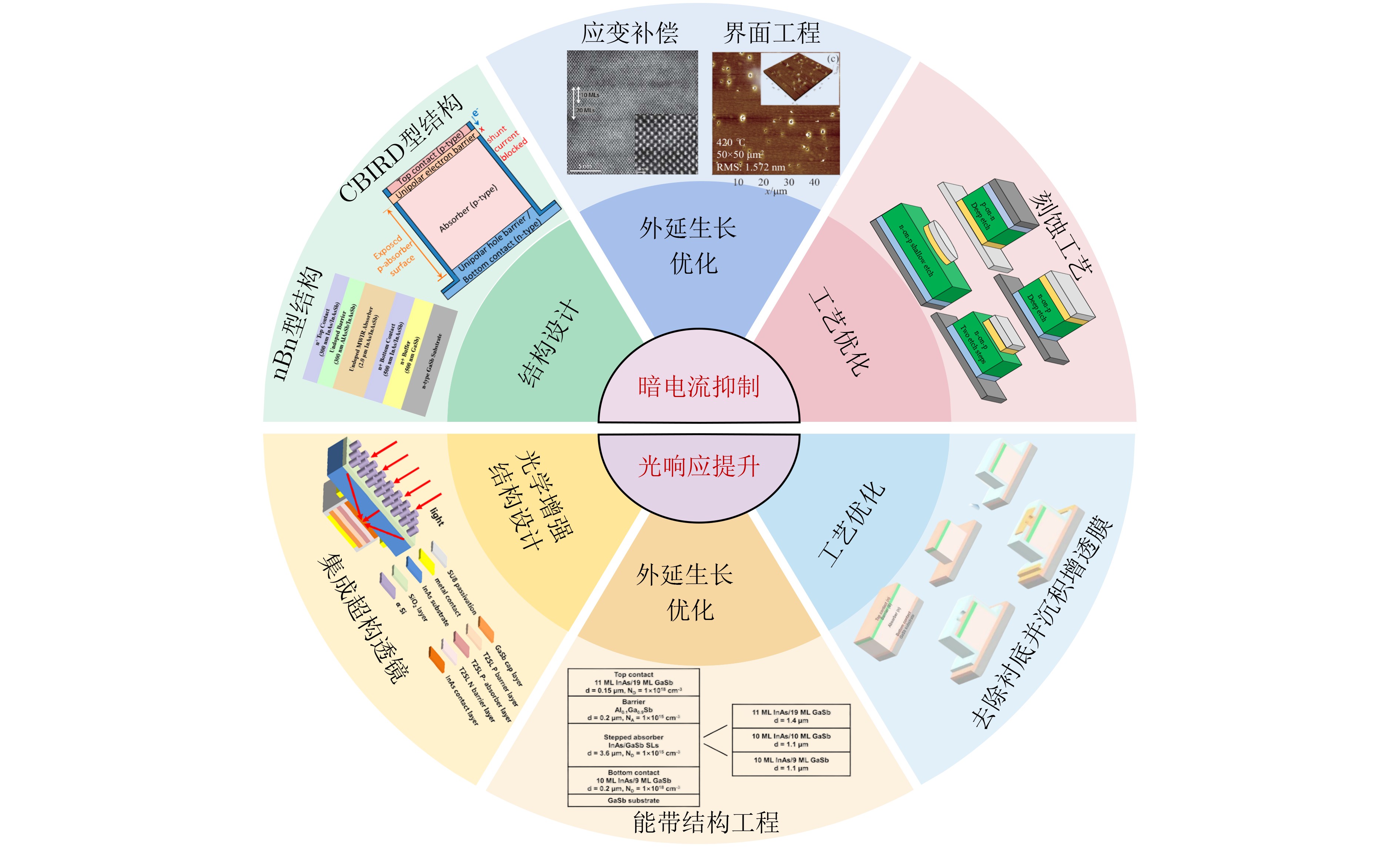
Abstract:Significance Mid-Wavelength Infrared (MWIR) detectors are widely used in civilian and military applications because of their high sensitivity and excellent temperature discrimination. Type-II SuperLattice (T2SL) materials, especially the InAs/GaSb and InAs/InAsSb systems, have become promising candidates for third-generation infrared photodetectors. This review systematically analyzes the research status and future trends of MWIR T2SL detector technology. It focuses on key photoelectric parameters, including Quantum Efficiency (QE), dark current density, and Specific Detectivity (D*). This work provides a reference for material selection and performance optimization in this rapidly developing field. Progress Considerable progress has been made in dark current suppression and photoresponse enhancement for MWIR T2SL detectors. For dark current suppression, advanced barrier structures, such as nBn, XBn, and M-structures, are designed through band-structure engineering. These structures effectively block majority-carrier transport while allowing efficient collection of photogenerated carriers. For instance, an nBn device with an AlAsSb/InAsSb superlattice barrier shows a dark current density of 2.01×10⁻⁵ A/cm2 at 150 K ( Fig. 2(c) ). Strain compensation and optimized epitaxial growth further reduce bulk dark current. One device achieves a dark current density of 4.5×10⁻⁷ A/cm2 at 140 K (Fig. 4(f) ). Device process optimization, including two-step etching and Zn-diffusion-based planar junction formation, also reduces surface leakage current (Fig. 5 ,Fig. 6 ). For photoresponse enhancement, the main strategies include micro/nano-optical structure integration, epitaxial growth optimization, and device process improvement. Monolithically integrated metalenses increase th,e peak responsivity to 9.01 A/W at 300 K (Fig. 7(d) ). Guided-mode resonance architectures enable a room-temperature External Quantum Efficiency (EQE) of approximately 60% (Fig. 8(c) ). Epitaxial optimization, including stepped absorption layers and interfacial graded doping, increases the QE to 59.4% at 150 K (Fig. 10(c) ). Device process optimization, such as substrate removal and Anti-Reflection (AR) coating deposition, also improves QE. An average QE of 63.7% is reported in the 3.7~4.8 μm range (Fig.13(c) ). Comparative analysis shows that InAs/GaSb detectors are mainly reported at 77~150 K, whereas InAs/InAsSb detectors show stronger potential for higher-temperature operation, especially near 150 K (Fig. 15 ,Fig. 16 ). Overall, at 150K, dark current densities are generally suppressed below 10–4 A/cm2, and peak QEs approach 70%.Conclusions T2SL materials, with tunable band structures and low Auger recombination rates, have become a core material platform for high-performance MWIR detection. Current studies have addressed key challenges in dark current suppression and photoresponse enhancement. Through advanced barrier design and device process optimization, dark current densities have been suppressed to the 10–6 A/cm2 level at approximately 150 K. Through optical and epitaxial engineering, QEs have been increased to approximately 60% or higher. The InAs/InAsSb material system is particularly promising for High-Operating-Temperature (HOT) applications. Prospects Future development will focus on four main directions. First, the HOT limit should be further increased, with the goal of maintaining diffusion-limited performance at 180 K or higher. Second, large-format Focal Plane Arrays (FPAs) should be developed based on highly uniform material growth through mature Molecular Beam Epitaxy (MBE), aiming for pixel operability higher than 99%. Third, multicolor and multispectral detection should be expanded by precisely tuning superlattice periods, enabling integrated dual-band or multiband MWIR detection with reduced crosstalk. Fourth, new device architectures and coupled physical mechanisms should be explored to extend detector performance and application boundaries. -
Key words:
- Type-II SuperLattice (T2SL) /
- Mid-Wavelength Infrared (MWIR) /
- InAs/GaSb /
- InAs/InAsSb
-
表 1 InAs/GaSb体系中波红外探测器性能参数对比
文献 温度(K) 截止波长(μm) 器件结构 暗电流密度
(A/cm2)量子效率(%) 比探测率
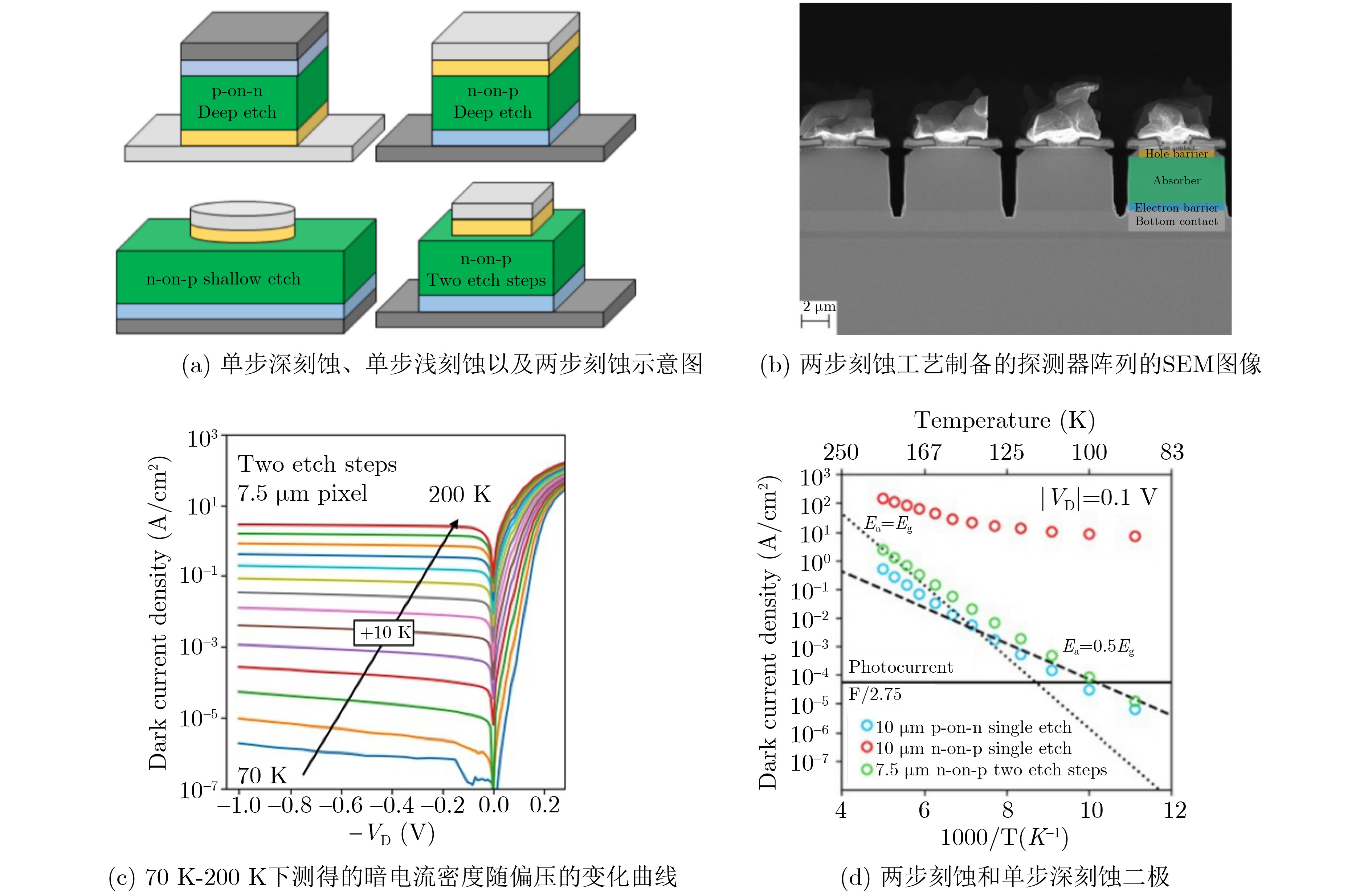
(cm·Hz1/2/W)[17] 120 5.2 nBn 2.00×10⁻⁵ / / [19] 100 5.0 n-on-p 8.80×10⁻⁵ / / [21] 300 5.0 BIRD 10.90 / 3.00×10⁹ [23] 150 6.0 nBn 3.90×10⁻⁵ 46.0 4.51×10¹⁰ [28] 300 7.5 pπMn 3.40×10⁻¹ 36.0 2.80×10⁹ [29] 77 5.7 pπMn 8.67×10⁻⁵ 42.5 3.90×10¹⁰ [30] 120 5.2 pin 6.00×10⁻⁵ 40.0 / [31] 77 5.2 pin 8.30×10⁻⁵ / / [32] 120 5.1 pπMn 1.00×10⁻⁶ 53.0 / [40] 77 5.1 nMπp 5.00×10⁻⁵ 38.0 1.00×10¹² [42] 150 6.0 / 6.50×10⁻⁶ 67.0 /  下载: 导出CSV
表 2 InAs/InAsSb体系中波红外探测器性能参数对比
文献 温度(K) 截止波长
(μm)器件结构 暗电流密度
(A/cm2)量子效率(%) 比探测率
(cm·Hz1/2/W)[16] 150 4.8 nBn 2.01×10⁻⁵ 58.8 6.47×10¹¹ [15] 150 6.0 nBn 4.50×10⁻⁵ 52.0 3.00×10¹¹ [18] 77 5.5 nBn 5.30×10⁻⁶ / 8.35×10¹¹ [20] 150 4.5 / 6.40×10⁻⁵ 49.0 2.00×10¹¹ [22] 296 5.0 nBn 1.00×10⁻¹ 60.0 1.20×10¹⁰ [24] 150 5.0 pBn 2.95×10⁻⁵ 59.4 1.24×10¹² [34] 150 5.5 pin 3.30×10⁻⁴ 55.0 1.20×10¹¹ [35] 150 5.0 p+-B-n 1.20×10⁻⁴ 29.0 1.20×10¹¹ [38] 150 6.0 XBn 3.50×10⁻⁵ 50.0 / [39] 150 6.0 CBIRD 1.14×10⁻⁵ 50.0 / [41] 300 3.5 pin 5.02×10⁻¹ 28.0 3.43×10⁹ [43] 77 5.2 pin 6.13×10⁻⁴ 34.6 / [44] 150 5.4 BIRD 3.00×10⁻⁵ 52.0 2.53×10¹¹ [47] 77 4.5 pBn 1.84×10⁻⁵ 63.7 8.65×10¹¹ 160 4.8 pBn 7.31×10⁻⁵ 59.8 4.96×10¹¹
下载: 导出CSV
-
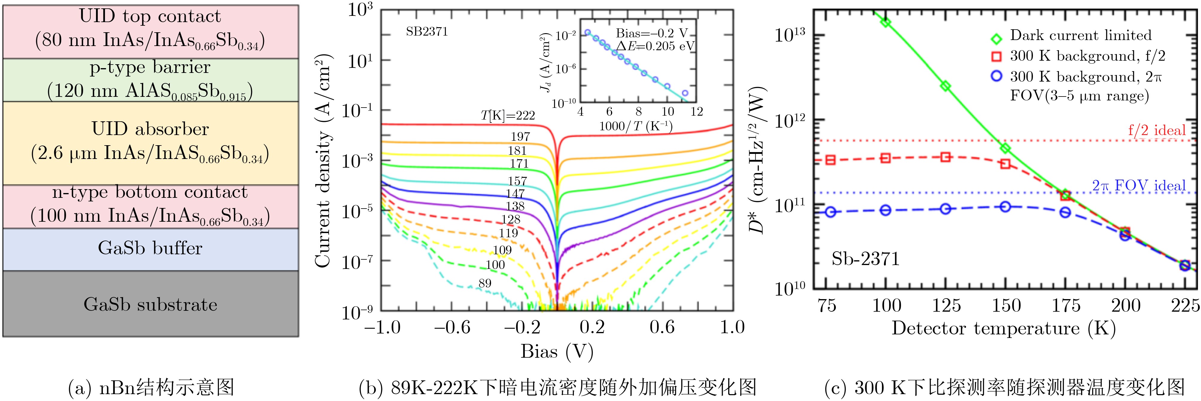
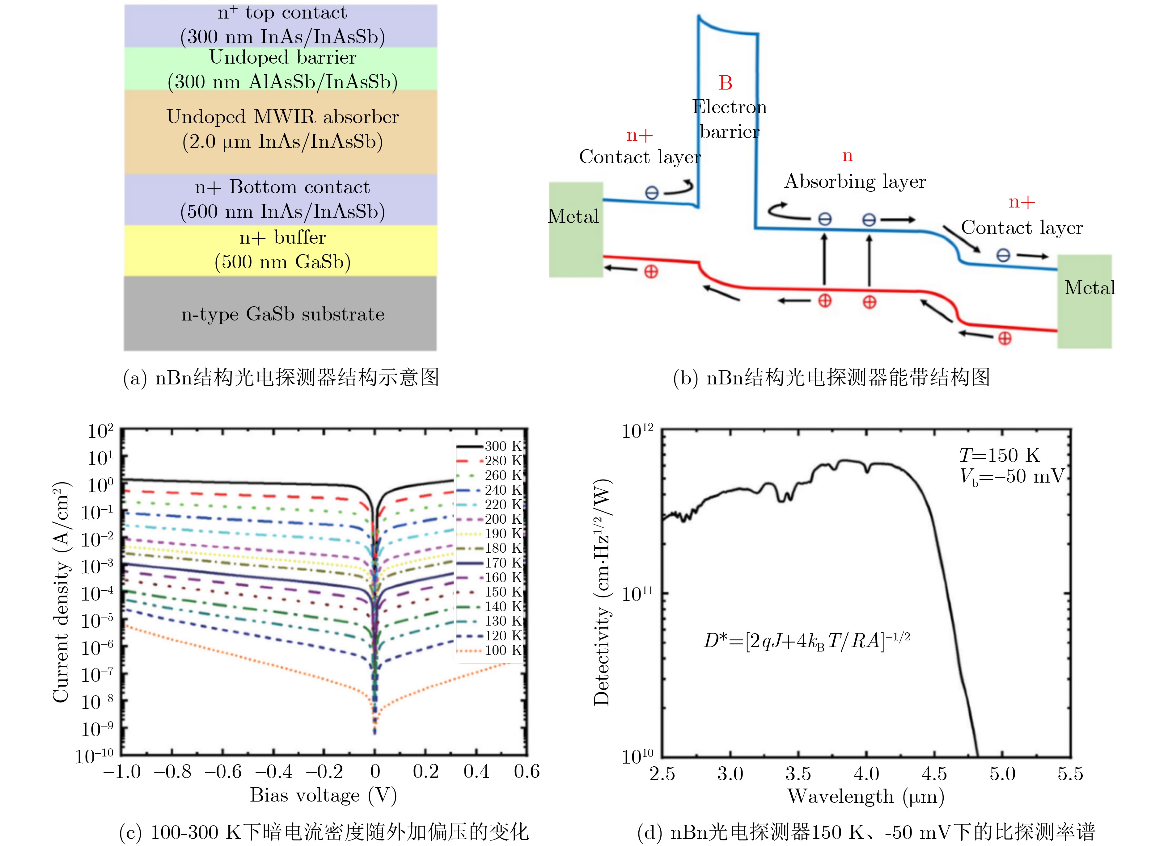
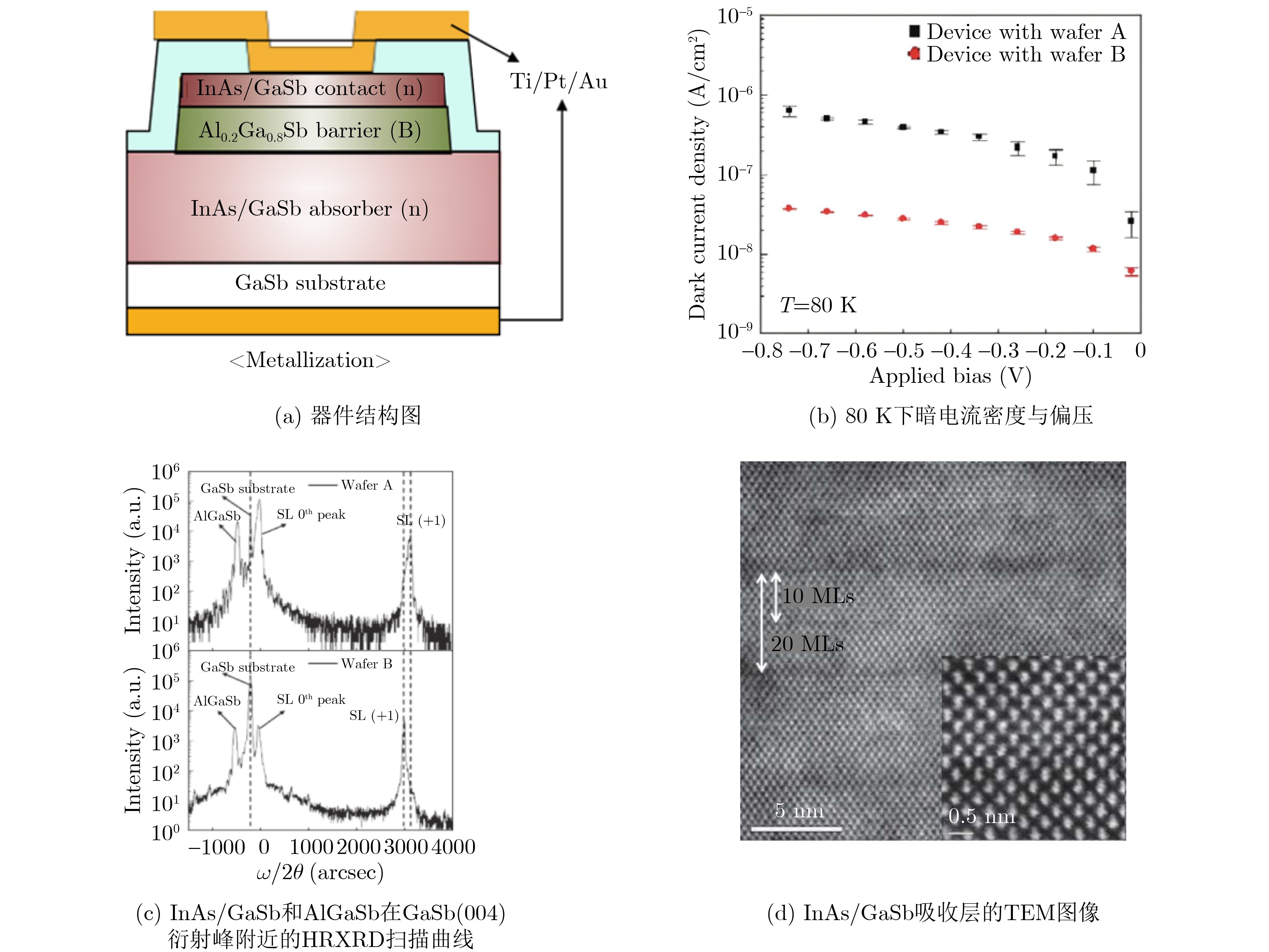
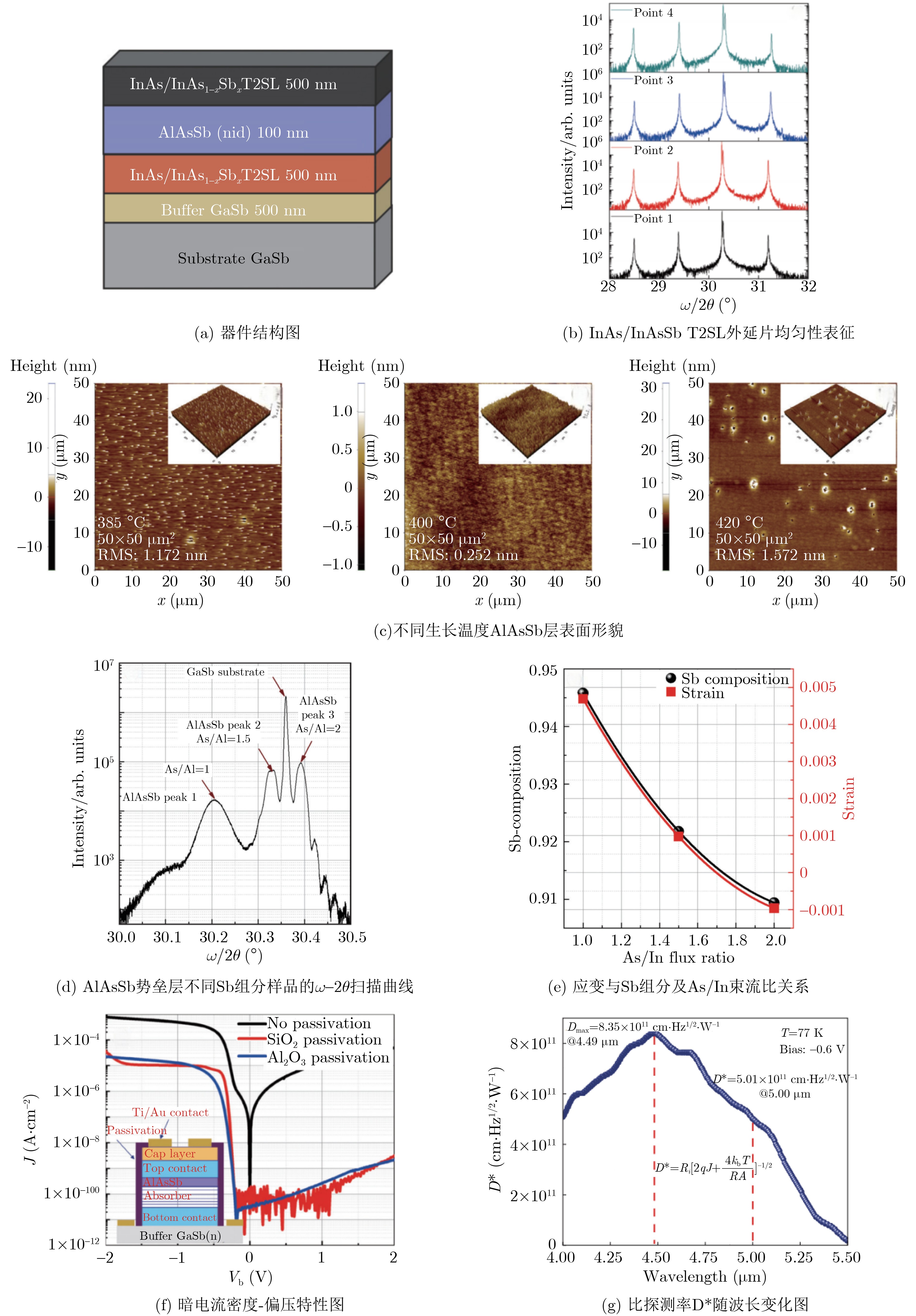
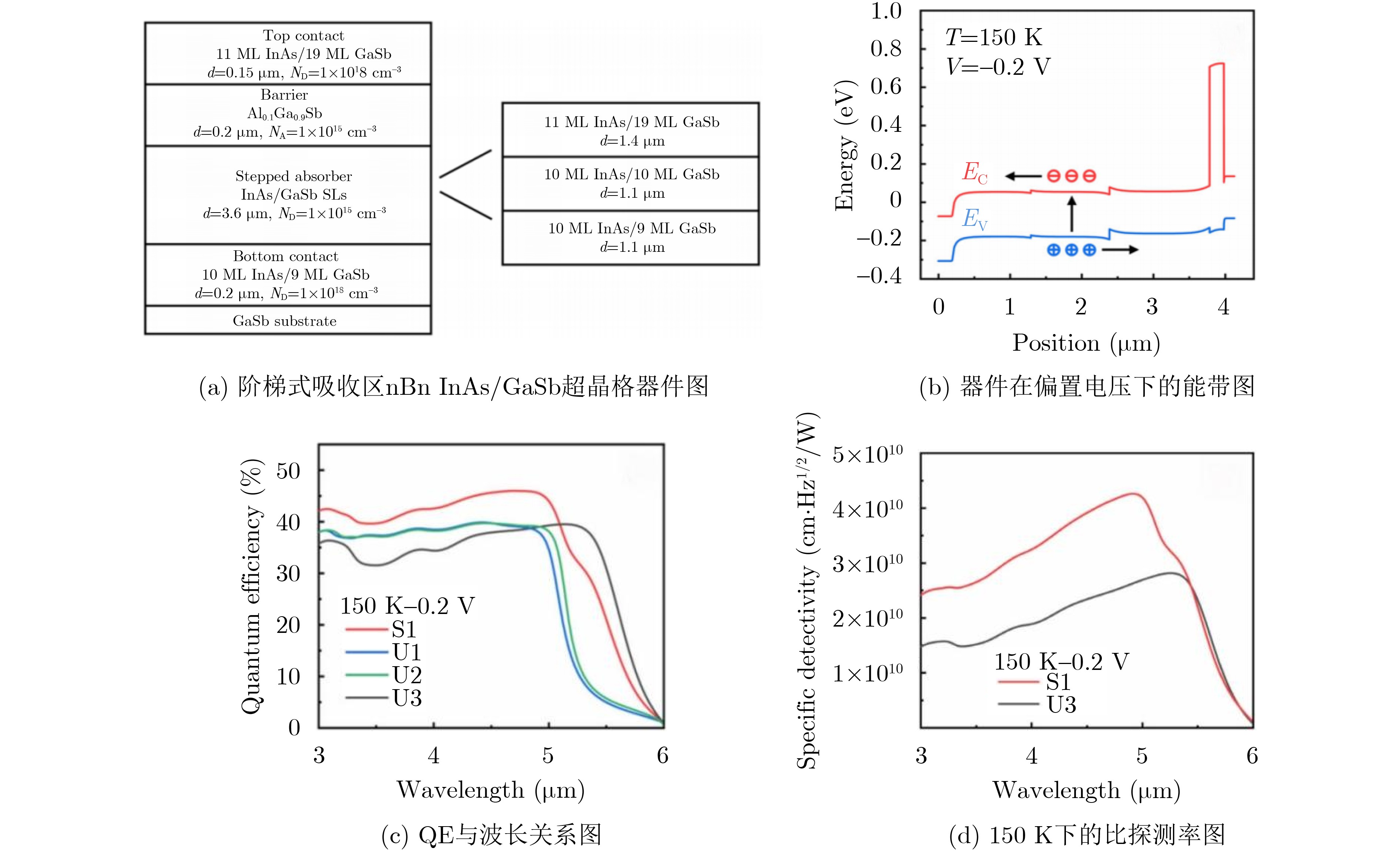
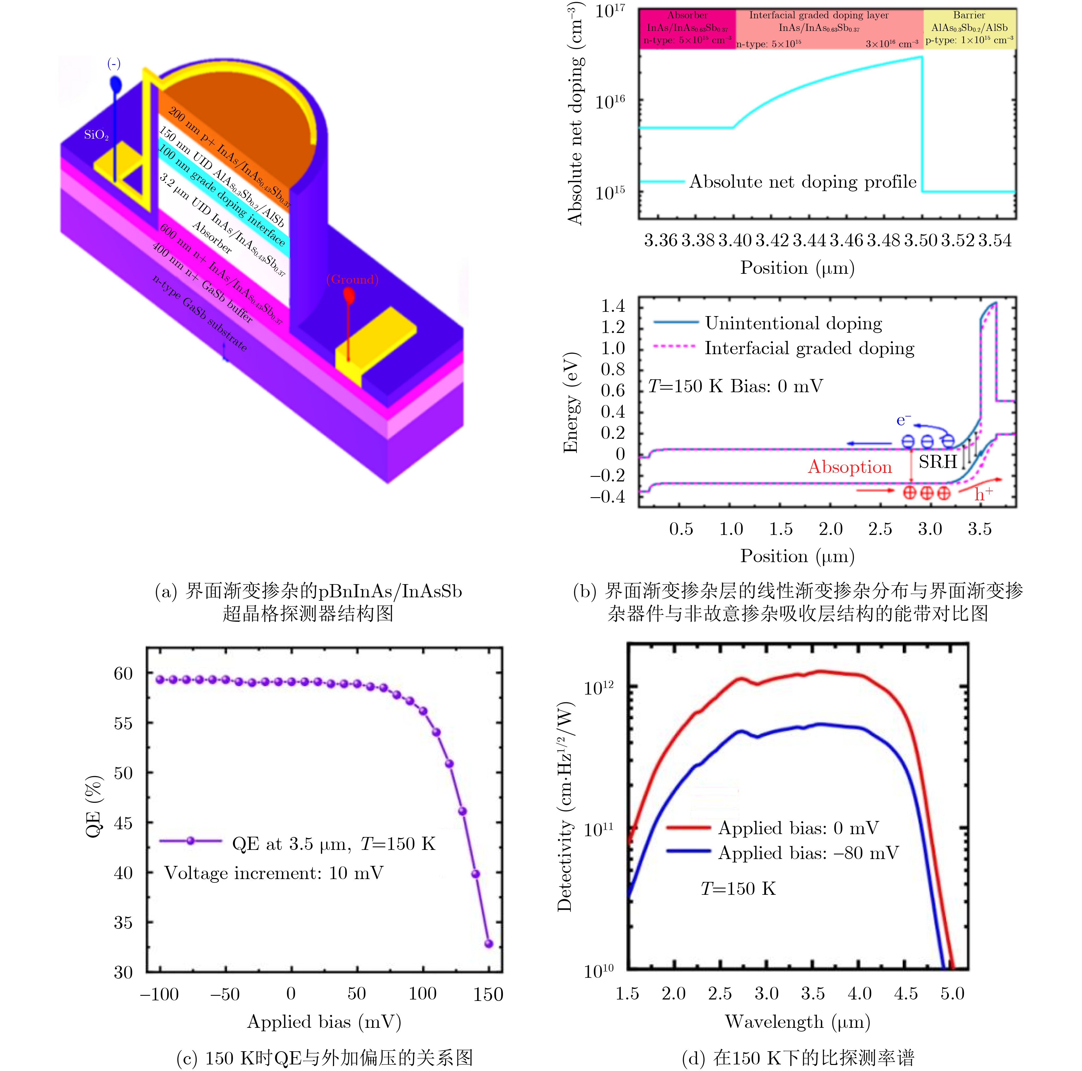
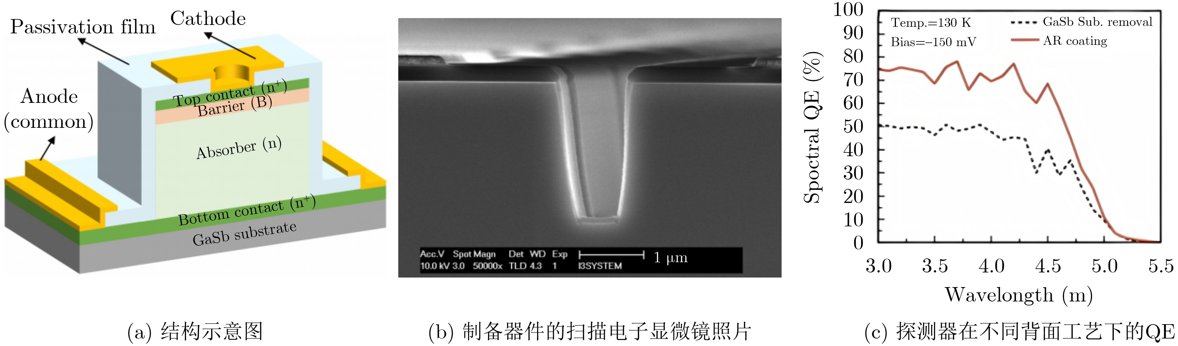
[1] SAI-HALASZ G A, TSU R, and ESAKI L. A new semiconductor superlattice[J]. Applied Physics Letters, 1977, 30(12): 651–653. doi: 10.1063/1.89273. [2] MAILHIOT C and SMITH D L. Electronic structure of (001) and (111) growth axis InAs-Ga1-x InxSb strained-layer superlattices[J]. Journal of Vacuum Science & Technology B: Microelectronics Processing and Phenomena, 1987, 5(4): 1268–1273. doi: 10.1116/1.583817. [3] 杨雪艳, 孙童, 关晓宁, 等. T2SL红外探测器高量子效率机理的研究进展[J]. 激光技术, 2024, 48(6): 822–831. doi: 10.7510/jgjs.issn.1001-3806.2024.06.007.YANG Xueyan, SUN Tong, GUAN Xiaoning, et al. Research progress on the high quantum efficiency mechanism of T2SL infrared detectors[J]. Laser Technology, 2024, 48(6): 822–831. doi: 10.7510/jgjs.issn.1001-3806.2024.06.007. [4] ALSHAHRANI D O, KESARIA M, ANYEBE E A, et al. Emerging type-II superlattices of InAs/InAsSb and InAs/GaSb for mid-wavelength infrared photodetectors[J]. Advanced Photonics Research, 2022, 3(2): 2100094. doi: 10.1002/adpr.202100094. [5] ROGALSKI A. New ternary alloy systems for infrared detectors[C]. SPIE 1845, Liquid and Solid State Crystals: Physics, Technology and Applications, Zakopane, Poland, 1993: 52–60. doi: 10.1117/12.156938. [6] WANG Xiaohua, LI Jingzhen, YAN Yong, et al. Dark current analysis of InAs/GaSb type II superlattice infrared detectors[J]. IEEE Transactions on Electron Devices, 2023, 70(11): 5517–5527. doi: 10.1109/ted.2023.3314574. [7] JONES R C. Performance of detectors for visible and infrared radiation[J]. Advances in Electronics and Electron Physics, 1953, 5: 1–96. doi: 10.1016/s0065-2539(08)60683-6. [8] SHI Qian, ZHANG Shukui, WANG Jianlu, et al. Progress on nBn infrared detectors[J]. Journal of Infrared and Millimeter Waves, 2022, 41(1): 139–150. doi: 10.11972/j.issn.1001-9014.2022.01.010. [9] KLIPSTEIN P C, BENNY Y, COHEN Y, et al. XBn and XBp detectors based on type II superlattices[J]. Journal of Electronic Materials, 2022, 51(9): 4752–4757. doi: 10.1007/s11664-022-09661-0. [10] KLIPSTEIN P C. Perspective on III-V barrier detectors[J]. Applied Physics Letters, 2022, 120(6): 060502. doi: 10.1063/5.0084100. [11] LI Mingluo, GUAN Xiaoning, YANG Xueyan, et al. nBp-type InAs/InAsSb midwave infrared detector with multistep absorption[J]. Infrared Physics & Technology, 2026, 152: 106159. doi: 10.1016/j.infrared.2025.106159. [12] JIANG Junkai, CHANG Faran, ZHOU Wenguang, et al. High-performance extended short-wavelength infrared PBn photodetectors based on InAs/GaSb/AlSb superlattices[J]. Chinese Physics B, 2023, 32(3): 038503. doi: 10.1088/1674-1056/acaa2e. [13] MARCHEWKA M, JAROSZ D, RUSZAŁA M, et al. Interfaces-engineered M-structure for infrared detectors[J]. Opto-Electronics Review, 2024, 32(2): e150183. doi: 10.24425/opelre.2024.150183. [14] TING D Z, SOIBEL A, KHOSHAKHLAGH A, et al. Complementary barrier infrared detector architecture for long-wavelength infrared InAs/InAsSb type-II superlattice[J]. Applied Sciences, 2022, 12(24): 12508. doi: 10.3390/app122412508. [15] TING D Z, SOIBEL A, KHOSHAKHLAGH A, et al. Mid-wavelength high operating temperature barrier infrared detector and focal plane array[J]. Applied Physics Letters, 2018, 113(2): 021101. doi: 10.1063/1.5033338. [16] 单一凡, 吴东海, 谢若愚, 等. 基于AlAsSb/InAsSb超晶格势垒的InAs/InAsSb Ⅱ类超晶格nBn中波红外探测器[J]. 红外与毫米波学报, 2024, 43(4): 450–456. doi: 10.11972/j.issn.1001-9014.2024.04.003.SHAN Yifan, WU Donghai, XIE Ruoyu, et al. Mid-wavelength infrared nBn photodetectors based on InAs/InAsSb type-II superlattice with an AlAsSb/InAsSb superlattice barrier[J]. Journal of Infrared and Millimeter Waves, 2024, 43(4): 450–456. doi: 10.11972/j.issn.1001-9014.2024.04.003. [17] LEE H J, KO S Y, KIM Y H, et al. Strain-induced the dark current characteristics in InAs/GaSb type-II superlattice for mid-wave detector[J]. Journal of Semiconductors, 2020, 41(6): 062302. doi: 10.1088/1674-4926/41/6/062302. [18] 刘炳锋, 祝连庆, 鹿利单, 等. 中波InAs/InAsSb超晶格红外探测器设计及势垒外延优化制备[J]. 红外与激光工程, 2025, 54(8): 20250340. doi: 10.3788/IRLA20250340.LIU Bingfeng, ZHU Lianqing, LU Lidan, et al. Design of mid-wavelength InAs/InAsSb superlattice infrared detectors and barrier epitaxial optimization[J]. Infrared and Laser Engineering, 2025, 54(8): 20250340. doi: 10.3788/IRLA20250340. [19] RAMOS D, DELMAS M, IVANOV R, et al. Two-step etch in n-on-p type-II superlattices for surface leakage reduction in mid-wave infrared megapixel detectors[J]. Opto-Electronics Review, 2023, 31(S1): e144556. doi: 10.24425/opelre.2023.144556. [20] LI Jiakai, SAROJ R K, SLIVKEN S, et al. High performance planar antimony-based superlattice photodetectors using zinc diffusion grown by MBE[J]. Photonics, 2022, 9(9): 664. doi: 10.3390/photonics9090664. [21] YUE Jiaxin, ZHANG Jinyu, QIN Le, et al. Enhancing mid-wavelength InAs/GaSb type II superlattice infrared detector with monolithically integrated metalens[J]. Optics Express, 2025, 33(15): 30948–30956. doi: 10.1364/OE.568141. [22] KAMBOJ A, NORDIN L, MUHOWSKI A J, et al. Room-temperature mid-wave infrared guided-mode resonance detectors[J]. IEEE Photonics Technology Letters, 2022, 34(11): 615–618. doi: 10.1109/LPT.2022.3175110. [23] YUAN Qi, LI Chuang, GUO Daqian, et al. High-performance midwave type-II superlattice infrared photodetectors with a stepped InAs/GaSb absorber[J]. IEEE Transactions on Electron Devices, 2023, 70(5): 2347–2351. doi: 10.1109/TED.2023.3256965. [24] ZHANG Ye, SHAN Yifan, CHANG Faran, et al. High operating temperature mid-wavelength infrared detectors based on InAs/InAsSb superlattices with electron block interfacial graded doping[J]. Optics Express, 2025, 33(17): 36672–36681. doi: 10.1364/oe.572457. [25] WU Yuyang, ZHANG Yahui, ZHANG Yi, et al. Dual strategy of modulating growth temperature and inserting ultrathin barrier to enhance the wave function overlap in type-II superlattices[J]. Nano Research, 2022, 15(6): 5626–5632. doi: 10.1007/s12274-022-4151-7. [26] MILOSAVLJEVIC M S, CARRASCO R A, NEWELL A T, et al. Spectroscopic ellipsometry measurement and analysis of the optical constants of InAs/InAsSb and InGaAs/InAsSb superlattices and their bulk constituents[J]. Journal of Applied Physics, 2025, 138(9): 093103. doi: 10.1063/5.0285129. [27] LEE H J, KIM Y C, EOM J H, et al. Development of MWIR and LWIR nBn photodetectors at i3system[C]. SPIE 12107, Infrared Technology and Applications XLVIII, Orlando, United States, 2022: 1210713. doi: 10.1117/12.2607715. [28] YAO Lingze, SHAN Yifan, XIE Ruoyu, et al. Room-temperature mid-wave infrared InAs/GaSb type-II superlattice photodetectors enhanced by ZnS anti-reflection coating[J]. Optical Materials, 2025, 165: 117155. doi: 10.1016/j.optmat.2025.117155. [29] ZHANG Shihao, HAO Hongyue, ZHANG Ye, et al. Mid-wavelength infrared planar junction photodetector based on InAs/GaSb Type-II superlattices[J]. Journal of Semiconductors, 2025, 46(11): 112404. doi: 10.1088/1674-4926/24120014. [30] ASPLUND C, MARCKS VON WÜRTEMBERG R, LANTZ D, et al. Performance of mid-wave T2SL detectors with heterojunction barriers[J]. Infrared Physics & Technology, 2013, 59: 22–27. doi: 10.1016/j.infrared.2012.12.004. [31] DELMAS M, DEBNATH M C, LIANG Baolai, et al. Material and device characterization of Type-II InAs/GaSb superlattice infrared detectors[J]. Infrared Physics & Technology, 2018, 94: 286–290. doi: 10.1016/j.infrared.2018.09.012. [32] HÖGLUND L, ASPLUND C, MARCKS VON WÜRTEMBERG R, et al. Manufacturability of type-II InAs/GaSb superlattice detectors for infrared imaging[J]. Infrared Physics & Technology, 2017, 84: 28–32. doi: 10.1016/j.infrared.2017.03.002. [33] DURLIN Q, PEREZ J P, CERUTTI L, et al. Midwave infrared barrier detector based on Ga-free InAs/InAsSb type-II superlattice grown by molecular beam epitaxy on Si substrate[J]. Infrared Physics & Technology, 2019, 96: 39–43. doi: 10.1016/j.infrared.2018.10.006. [34] WU Donghai, DURLIN Q, DEHZANGI A, et al. High quantum efficiency mid-wavelength infrared type-II InAs/InAs1-xSbx superlattice photodiodes grown by metal-organic chemical vapor deposition[J]. Applied Physics Letters, 2019, 114(1): 011104. doi: 10.1063/1.5058714. [35] SHE Lifang, JIANG Junkai, CHEN Weiqiang, et al. Mid-wave infrared p+-B-n InAs/InAsSb type-II superlattice photodetector with an AlAsSb/InAsSb superlattice barrier[J]. Infrared Physics & Technology, 2022, 121: 104015. doi: 10.1016/j.infrared.2021.104015. [36] CAO Peng, WANG Tiancai, PENG Hongling, et al. Mid-wavelength nBn photodetector with high operating temperature and low dark current based on InAs/InAsSb superlattice absorber[J]. Chinese Optics Letters, 2024, 22(1): 012502. doi: 10.3788/col202422.012502. [37] 刘炳锋, 祝连庆, 鹿利单, 等. nBn型高温中波InAs/InAsSb超晶格红外焦平面探测器[J]. 光学学报, 2025, 45(7): 0712001. doi: 10.3788/AOS241909.LIU Bingfeng, ZHU Lianqing, LU Lidan, et al. High operating temperature InAs/InAsSb Type-II superlattice mid-wave infrared nBn focal plane detectors[J]. Acta Optica Sinica, 2025, 45(7): 0712001. doi: 10.3788/AOS241909. [38] BOUSCHET M, AROUNASSALAME V, RAMIANDRASOA A, et al. Temperature dependence study of electrical and electro-optical performances of midwave infrared Ga-free T2SL barrier photodetector[J]. Applied Sciences, 2022, 12(20): 10358. doi: 10.3390/app122010358. [39] TING D Z, SOIBEL A, KHOSHAKHLAGH A, et al. The effect of p-doping in mid-and long-wavelength InAs/InAsSb superlattice complementary barrier infrared detectors[J]. Applied Physics Letters, 2024, 125(19): 191106. doi: 10.1063/5.0236130. [40] SUN Yaoyao, WANG Guowei, HAN Xi, et al. 320×256 high operating temperature mid-infrared focal plane arrays based on type-II InAs/GaSb superlattice[J]. Superlattices and Microstructures, 2017, 111: 783–788. doi: 10.1016/j.spmi.2017.07.037. [41] JIANG Junkai, WANG Guowei, WU Donghai, et al. High-performance infrared photodetectors based on InAs/InAsSb/AlAsSb superlattice for 3.5 µm cutoff wavelength spectra[J]. Optics Express, 2022, 30(21): 38208–38215. doi: 10.1364/OE.469147. [42] DELMAS M, HÖGLUND L, IVANOV R, et al. HOT SWaP and HD detectors based on Type-II superlattices at IRnova[C]. SPIE 12107, Infrared Technology and Applications XLVIII, Orlando, United States, 2022: 121070R. doi: 10.1117/12.2618752. [43] HAO Ruiting, REN Yang, LIU Sijia, et al. Fabrication and characterization of high lattice matched InAs/InAsSb superlattice infrared photodetector[J]. Journal of Crystal Growth, 2017, 470: 33–36. doi: 10.1016/j.jcrysgro.2017.03.052. [44] TING D Z, RAFOL S B, KEO S A, et al. InAs/InAsSb type-II superlattice mid-wavelength infrared focal plane array with significantly higher operating temperature than InSb[J]. IEEE Photonics Journal, 2018, 10(6): 6804106. doi: 10.1109/JPHOT.2018.2877632. [45] KLIPSTEIN P C, ARMON E, AVNON E, et al. HOT MWIR technology at SCD[C]. SPIE 12107, Infrared Technology and Applications XLVIII, Orlando, United States, 2022: 121070Q. doi: 10.1117/12.2615622. [46] KOPYTKO M, MADEJCZYK P, MURAWSKI K, et al. Comparison of type II superlattice InAs/InAsSb barrier detectors operating in the mid-wave infrared range[J]. Journal of Applied Physics, 2024, 136(1): 014501. doi: 10.1063/5.0202170. [47] HUANG Jianliang, YAN Shaolong, XUE Ting, et al. Mid-wavelength InAs/InAsSb superlattice photodetector with background limited performance temperature higher than 160 K[J]. IEEE Transactions on Electron Devices, 2022, 69(8): 4392–4395. doi: 10.1109/TED.2022.3186648. -

 下载:
下载:


图(17) / 表(2)
计量
- 文章访问数: 553
- HTML全文浏览量: 195
- PDF下载量: 74
- 被引次数: 0
