

A Method for Parallel Testing of Interlayer Vias in Monolithic 3D Integrated Circuits
-
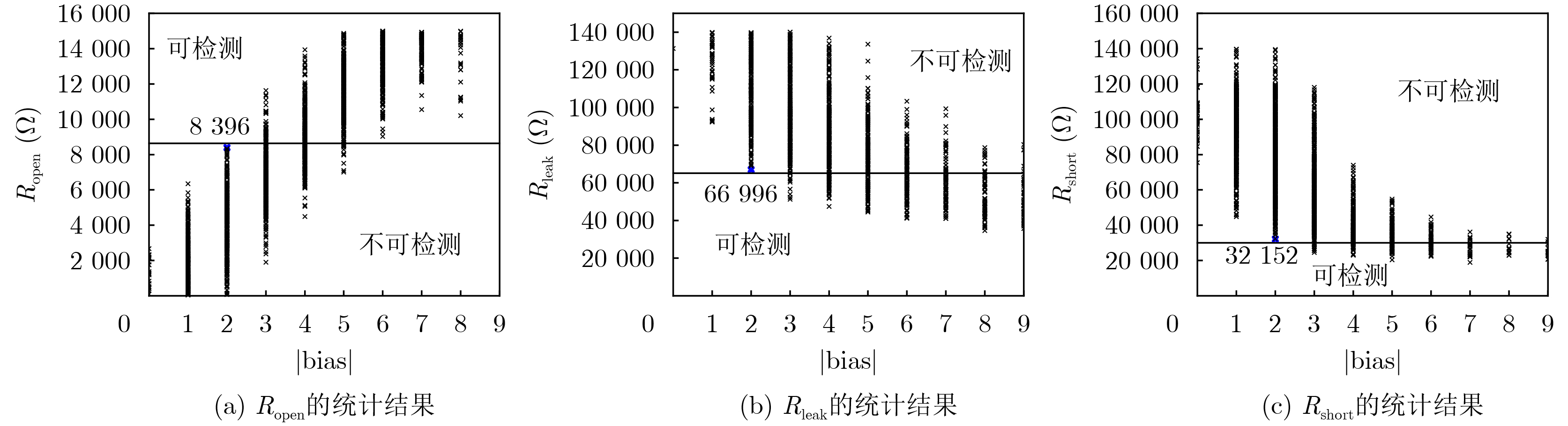
摘要: 在单片三维集成电路中,单片层间通孔(MIV)是实现垂直互连的关键结构,其制造缺陷会严重影响芯片可靠性。然而,面对MIV数量庞大、电气参数微小、故障类型多样的特点,实现高精度、低开销的测试是一个重要挑战。该文提出一种基于时间数字转换器(TDC)的MIV并行测试方法。通过行列分组将待测MIV构建成行或列的测试链,并通过数控延迟线(DCDL)来生成具有特定相位关系的测试激励信号。利用TDC测量电路的响应,并通过分析响应序列的规律性偏差,可以实现MIV硬故障和小延迟故障的测试。仿真结果表明,该方法在45 nm工艺下可检测阻值高于8.4 kΩ的开路故障,低于67 kΩ的泄漏故障以及低于32 kΩ的短路故障,而且测试结果在不同工艺-电压-温度(PVT)条件下保持稳定。与现有方案相比,该方法在检测精度、条件鲁棒性及硬件开销方面展现出更好的综合性能,为高密度M3D IC的MIV测试提供了一种有效解决方案。Abstract:
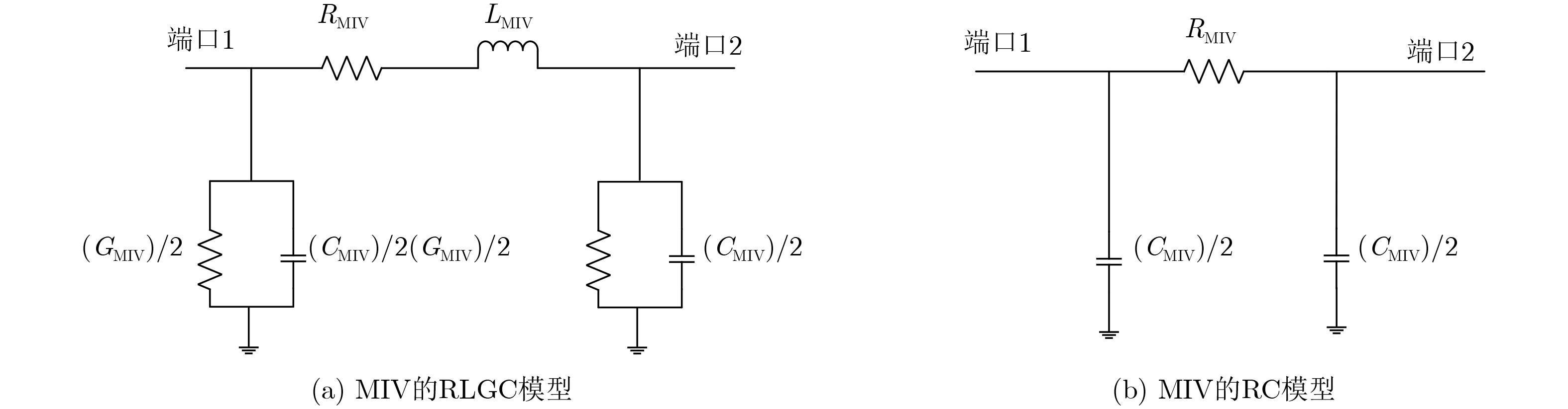
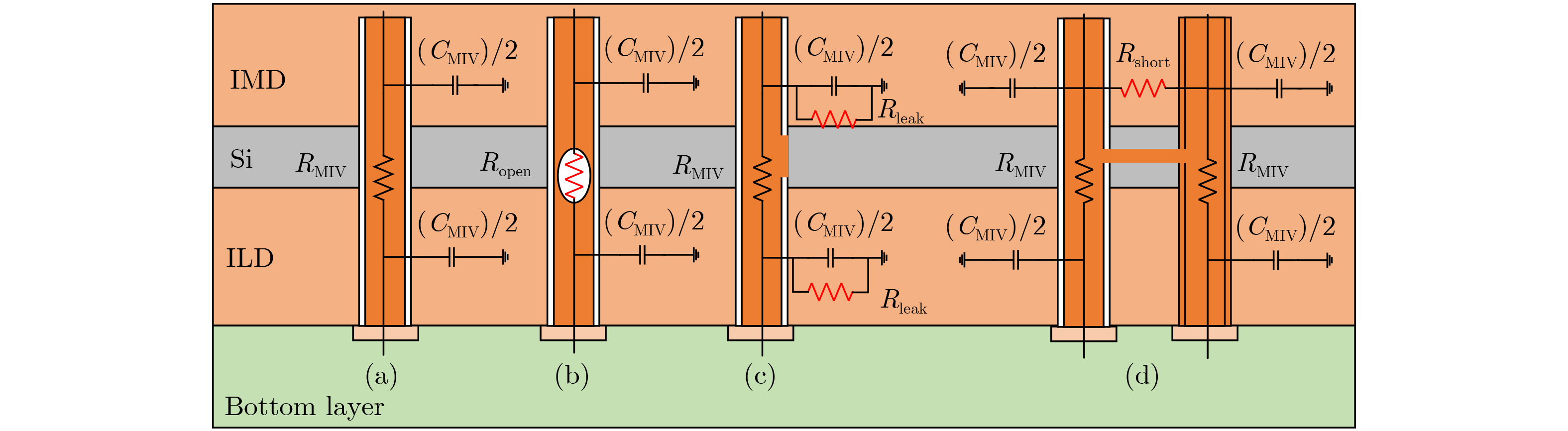
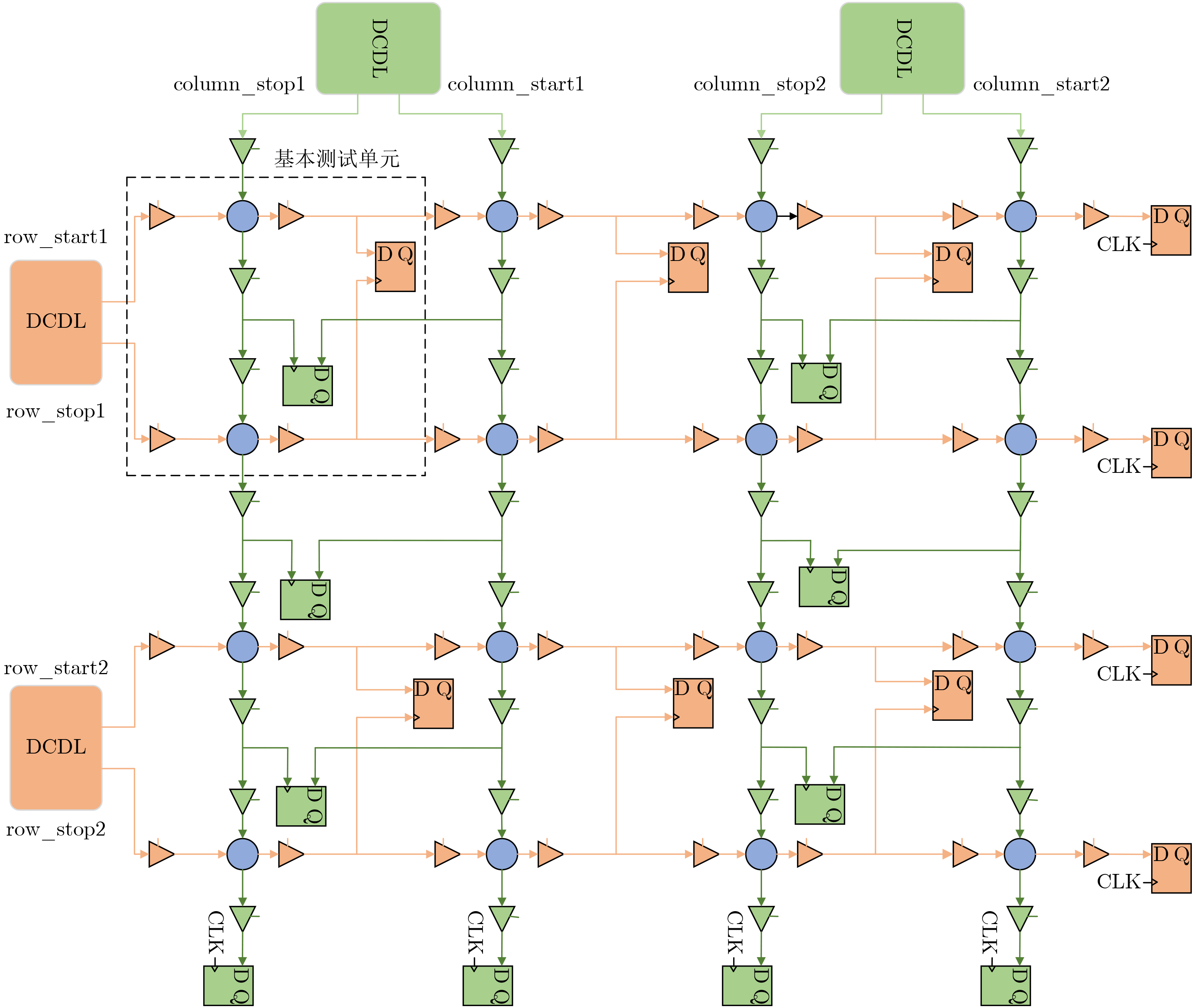
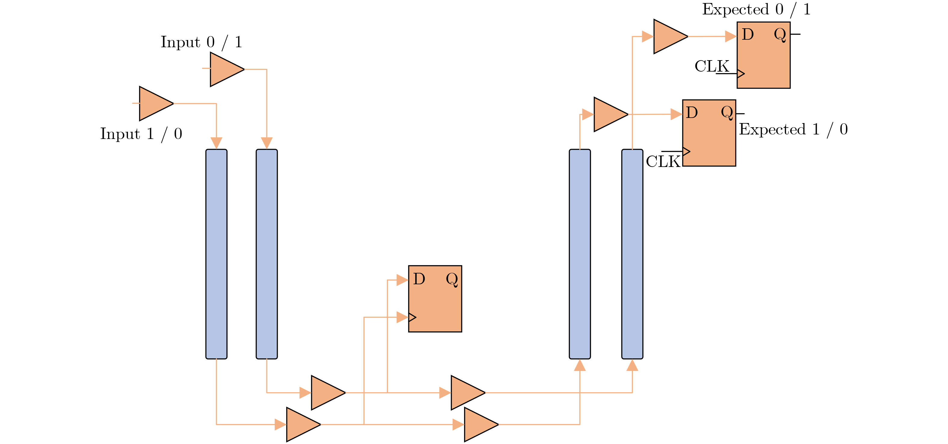
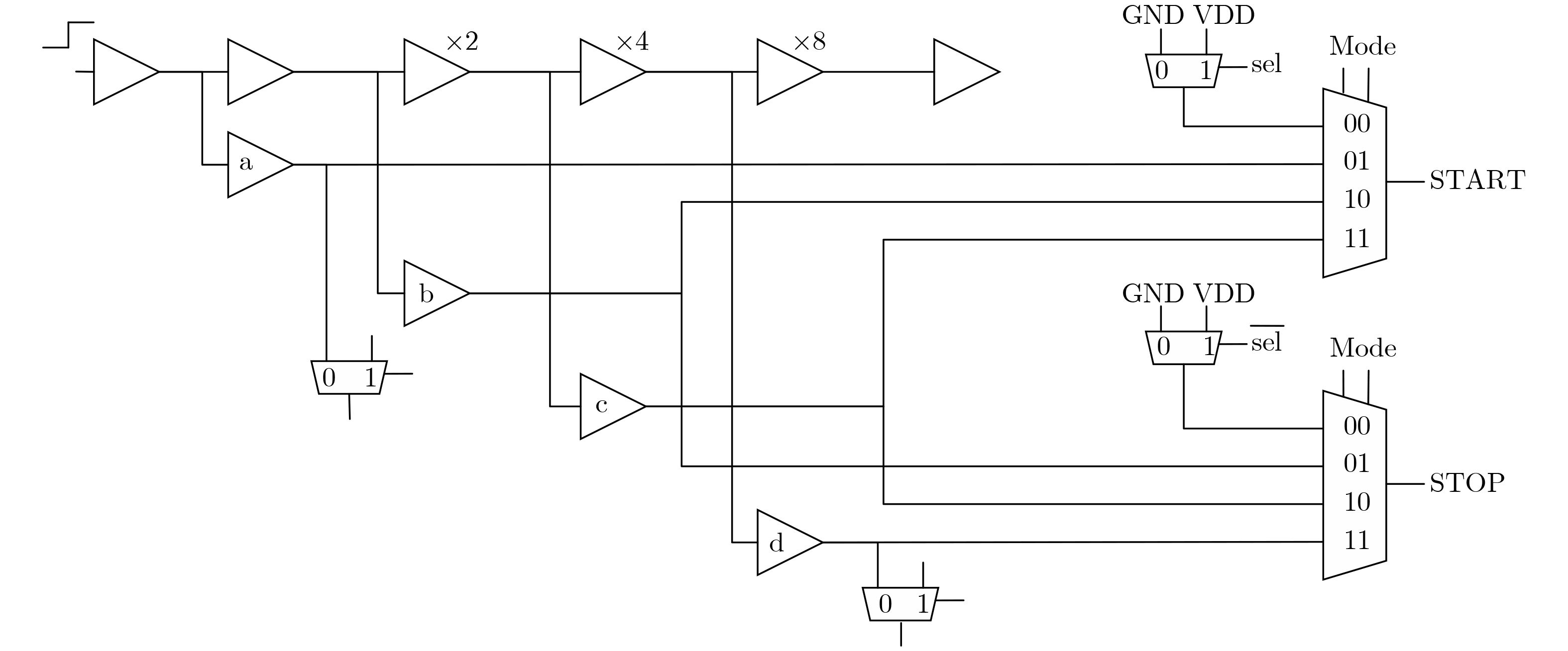
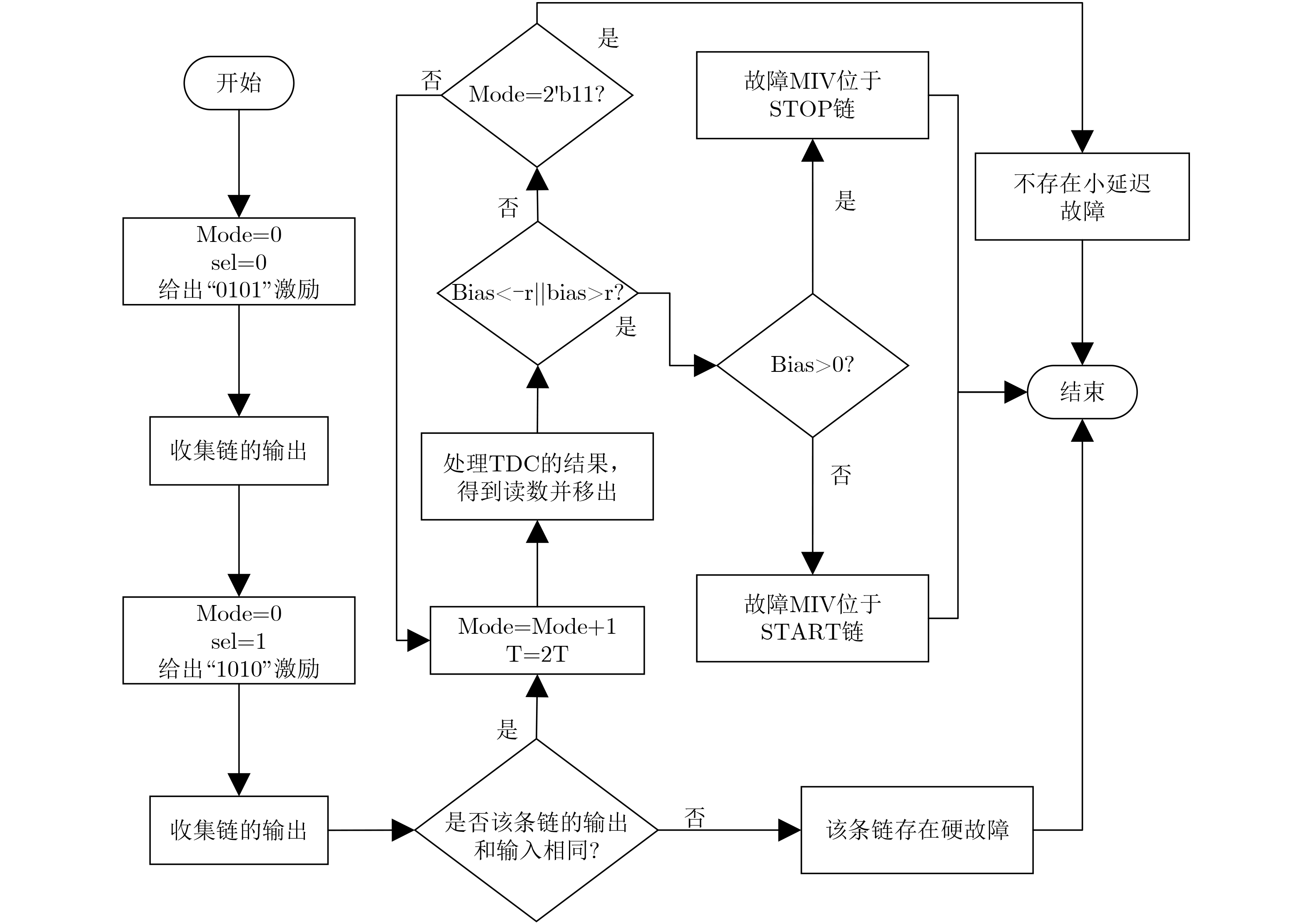
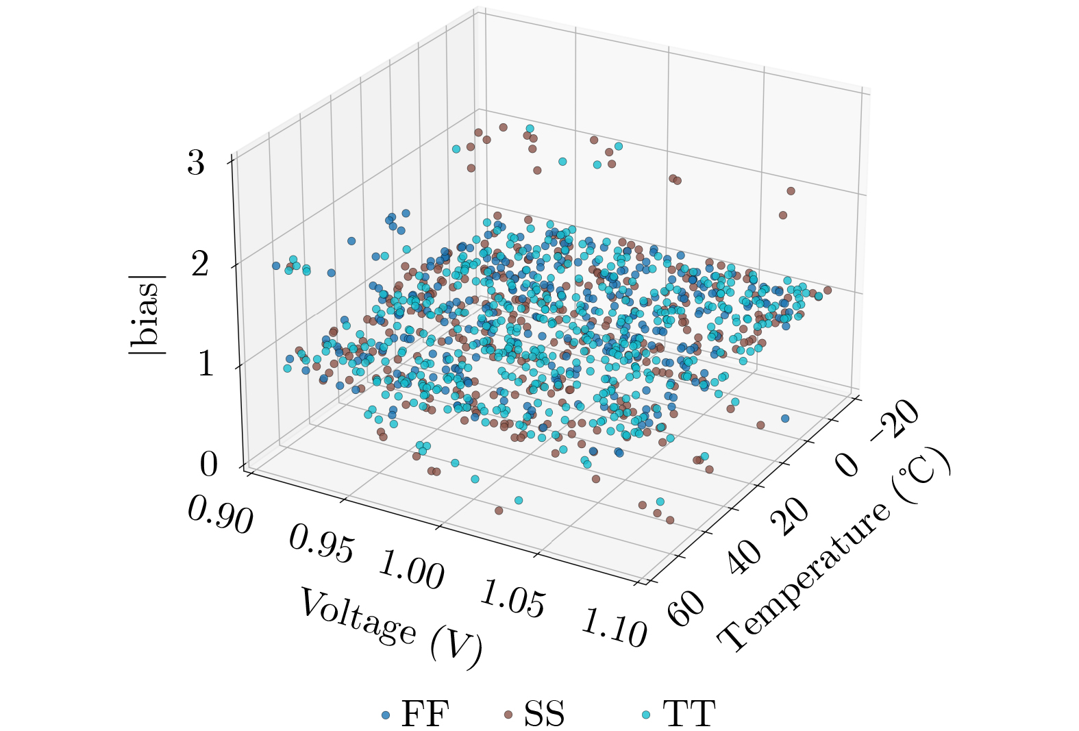
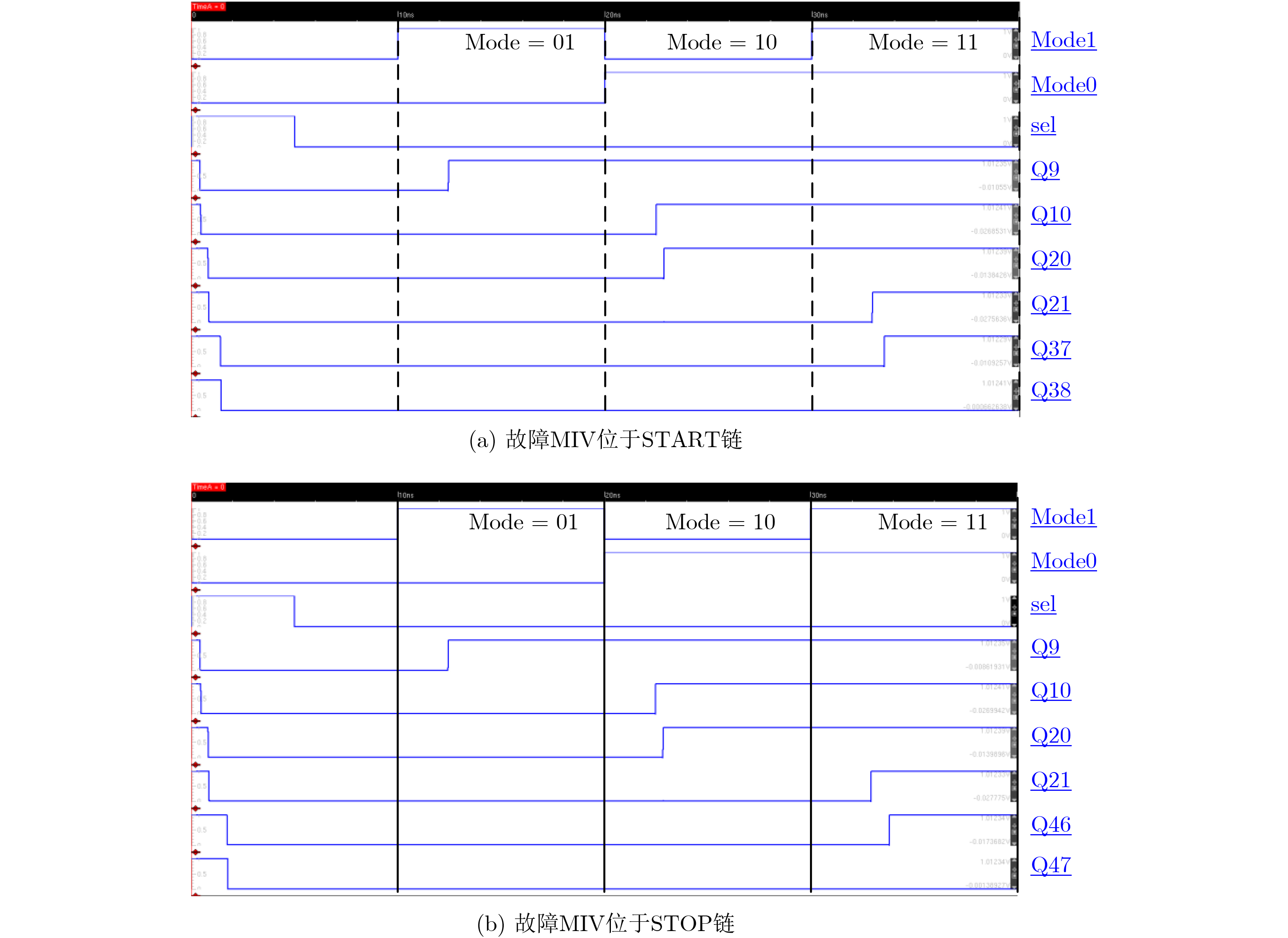
Objective As device dimensions in conventional two-dimensional integrated circuits approach fundamental physical limits, further improvements in performance and integration density face major challenges. Monolithic Three-Dimensional Integrated Circuits (M3D ICs), in which multiple active device layers are sequentially stacked on a single wafer, provide an effective way to address these limitations. In M3D ICs, Monolithic Inter-tier Vias (MIVs) are used to realize vertical interconnections between device tiers. Compared with Through-Silicon Vias (TSVs), MIVs have much smaller dimensions, lower parasitic capacitance, and shorter interconnect delay. However, because of their small electrical variations and large numbers, defects are mainly manifested as subtle delay shifts. This places stringent demands on test accuracy, efficiency, and robustness to Process, Voltage, and Temperature (PVT) variations. Existing MIV test methods have limited scalability, show strong sensitivity to PVT variations, and have difficulty achieving both small-delay defect detection and fault localization in large-scale arrays. To address these issues, a parallel MIV test method based on a Time-to-Digital Converter (TDC) is presented to enable efficient and reliable testing of large MIV arrays with low area and time overhead. Methods Large-scale MIVs are logically organized into a two-dimensional array. Each basic test cell consists of a device-under-test MIV, a tri-state buffer, and a D flip-flop, and multiple cells are cascaded to form row and column test chains. By systematically exploiting the inherent input capacitance mismatch between the data and clock terminals of the D flip-flop, an embedded TDC structure that incorporates the MIV under test is constructed. Test stimuli are generated by a Digitally Controlled Delay Line (DCDL), which produces START and STOP pulse signals with multiplicatively adjustable phase differences. These signals are injected into different propagation paths of the test chains, so that time quantization is achieved through a signal-chasing mechanism. Structural symmetry between the test chains is used to reduce the effect of PVT variations. As the phase difference between START and STOP is progressively amplified, multiple TDC readings are collected to characterize defect-induced small delay variations and to distinguish them from measurement noise and PVT-induced fluctuations. After fault information is obtained for individual test chains, cross-analysis of the row and column test results is used to localize faults within the two-dimensional MIV array. Results and Discussions Simulation results based on the Nangate 45 nm standard cell library show that, under fault-free conditions, TDC readings obtained at different phase-difference settings exhibit a stable linear proportional relationship ( Fig. 7 ). Extensive Monte Carlo simulations are conducted to determine a robust deviation tolerance threshold of 2, which effectively separates normal variations caused by PVT fluctuations from abnormal shifts induced by defects. Fault-injection experiments confirm that small-delay defects occurring in both the START chain and the STOP chain can be effectively detected and distinguished (Fig. 8 ). In terms of quantitative detection capability, the minimum detectable resistive open defect is approximately 8.4 kW, whereas the maximum detectable leakage defect and resistive short defect are about 67 kW and 32 kW, respectively, outperforming existing methods (Fig. 9 ). Moreover, the row-column decomposition architecture effectively alleviates the increase in test time as the MIV array size grows, which substantially reduces the overall test overhead. Area evaluation indicates that the average area overhead of the embedded built-in self-test structure is only 5.594 µm2 per MIV, which makes the method suitable for high-density M3D integration.Conclusions A parallel testing approach based on a TDC is presented for large-scale MIV arrays. By combining row-column decomposition, phase-difference multiplication, and a proportional deviation-based decision mechanism, efficient detection and accurate localization of both hard faults and small-delay defects are achieved. Structural symmetry within the test chains effectively improves robustness to PVT variations. Simulation results confirm that the proposed method can reliably detect resistive open, leakage, and short defects while maintaining low area and time overhead. Compared with existing techniques, the proposed method achieves a favorable balance among test accuracy, robustness to PVT variations, test efficiency, and hardware cost. Owing to its scalability and practical feasibility, it provides an effective and reliable solution for MIV testing in advanced M3D ICs. -
表 1 仿真参数
参数 值 电压VDD(V) 0.9−1.1 温度(℃) –20-60 Ropen范围(kΩ) 0-15 Rleak范围(kΩ) 10-70 Rshort范围(kΩ) 10-140 CD均值(fF) 0.955 Cclk均值(fF) 0.864  下载: 导出CSV
-
[1] 张芊帆, 何茜, 田雨, 等. 3D IC封装技术中硅通孔研究进展综述[J]. 电子与信息学报, 2025, 47(9): 3057–3069. doi: 10.11999/JEIT250377.ZHANG Qianfan, HE Xi, TIAN Yu, et al. Review of research progress on TSV technology in 3D IC packaging[J]. Journal of Electronics & Information Technology, 2025, 47(9): 3057–3069. doi: 10.11999/JEIT250377. [2] 卢美璇, 许浩博, 王颖, 等. 芯粒集成芯片架构-封装协同设计[J]. 电子与信息学报, 2025, 47(9): 2994–3009. doi: 10.11999/JEIT250626.LU Meixuan, XU Haobo, WANG Ying, et al. Co-design of architecture and packaging in chiplet[J]. Journal of Electronics & Information Technology, 2025, 47(9): 2994–3009. doi: 10.11999/JEIT250626. [3] LU Tiantao, SERAFY C, YANG Zhiyuan, et al. TSV-based 3-D ICs: Design methods and tools[J]. IEEE Transactions on Computer-Aided Design of Integrated Circuits and Systems, 2017, 36(10): 1593–1619. doi: 10.1109/TCAD.2017.2666604. [4] RADU I, GAUDIN G, VAN DEN DAELE W, et al. Novel low temperature 3D wafer stacking technology for high density device integration[C]. 2013 Proceedings of the European Solid-State Device Research Conference (ESSDERC), Bucharest, Romania, 2013: 151–154. doi: 10.1109/ESSDERC.2013.6818841. [5] RADU I, NGUYEN B Y, GAUDIN G, et al. 3D monolithic integration: Stacking technology and applications[C]. 2015 International Conference on IC Design & Technology (ICICDT), Leuven, Belgium, 2015: 1–3. doi: 10.1109/ICICDT.2015.7165915. [6] BISHOP M D, WONG H S P, MITRA S, et al. Monolithic 3-D integration[J]. IEEE Micro, 2019, 39(6): 16–27. doi: 10.1109/MM.2019.2942982. [7] VIVET P, THURIÈS S, BILLOINT O, et al. Monolithic 3D: An alternative to advanced CMOS scaling, technology perspectives and associated design methodology challenges[C]. 2018 25th IEEE International Conference on Electronics, Circuits and Systems (ICECS), Bordeaux, France, 2018: 157–160. doi: 10.1109/ICECS.2018.8617955. [8] KONERU A, KANNAN S, and CHAKRABARTY K. Impact of electrostatic coupling and wafer-bonding defects on delay testing of monolithic 3D integrated circuits[J]. ACM Journal on Emerging Technologies in Computing Systems (JETC), 2017, 13(4): 54. doi: 10.1145/3041026. [9] KONERU A, KANNAN S, and CHAKRABARTY K. Impact of wafer-bonding defects on Monolithic 3D integrated circuits[C]. 2016 IEEE 25th Conference on Electrical Performance of Electronic Packaging and Systems (EPEPS), San Diego, USA, 2016: 91–94. doi: 10.1109/EPEPS.2016.7835425. [10] 陈田, 章云飞, 刘军, 等. 基于可重配置环形振荡器的TSV诊断方法[J]. 微电子学与计算机, 2025, 42(3): 92–99. doi: 10.19304/J.ISSN1000-7180.2024.0150.CHEN Tian, ZHANG Yunfei, LIU Jun, et al. A TSV diagnosis method based on reconfigurable ring oscillator[J]. Microelectronics & Computer, 2025, 42(3): 92–99. doi: 10.19304/J.ISSN1000-7180.2024.0150. [11] LIU Xiaoting, ZHANG Xuewei, HONG Haofei, et al. A high-precision delay faults testing technique based on the improved DWR structure[C]. 2023 8th International Conference on Integrated Circuits and Microsystems (ICICM), Nanjing, China, 2023: 240–245. doi: 10.1109/ICICM59499.2023.10365804. [12] LIU Jun, CHENG Songren, CHEN Tian, et al. A self-biased current reference source-based pre-bond TSV test solution[J]. IEEE Transactions on Very Large Scale Integration (VLSI) Systems, 2024, 32(4): 774–781. doi: 10.1109/TVLSI.2023.3344272. [13] 窦贤锐, 梁华国, 黄正峰, 等. MOS管选通的硅通孔键合前测试[J]. 电子与信息学报, 2025, 47(9): 3286–3291. doi: 10.11999/JEIT250285.DOU Xianrui, LIANG Huaguo, HUANG Zhengfeng, et al. MOS-gated prebond through-silicon via testing[J]. Journal of Electronics & Information Technology, 2025, 47(9): 3286–3291. doi: 10.11999/JEIT250285. [14] NI Tianming, CHANG Hao, SONG Tai, et al. Non-intrusive online distributed pulse shrinking-based interconnect testing in 2.5D IC[J]. IEEE Transactions on Circuits and Systems II: Express Briefs, 2020, 67(11): 2657–2661. doi: 10.1109/TCSII.2019.2962824. [15] KONERU A and CHAKRABARTY K. An interlayer interconnect BIST and diagnosis solution for monolithic 3-D ICs[J]. IEEE Transactions on Computer-Aided Design of Integrated Circuits and Systems, 2020, 39(10): 3056–3066. doi: 10.1109/TCAD.2019.2935410. [16] CHAUDHURI A, BANERJEE S, PARK H, et al. Built-in self-test for inter-layer vias in monolithic 3D ICs[C]. 2019 IEEE European Test Symposium (ETS), Baden-Baden, Germany, 2019: 1–6. doi: 10.1109/ETS.2019.8791515. [17] CHEN Tian, DING Ruiyuan, LIU Jun, et al. A scan-chain-based built-in self-test for ILV in monolithic 3-D ICs[J]. IEEE Transactions on Instrumentation and Measurement, 2024, 73: 3536013. doi: 10.1109/TIM.2024.3472787. [18] FANG Xu and ZHAO Xiaofeng. A post-bond ILV test method in monolithic 3-D ICs[J]. IEEE Transactions on Very Large Scale Integration (VLSI) Systems, 2024, 32(12): 2377–2388. doi: 10.1109/TVLSI.2024.3450452. [19] XIAO Ziwen, DU Lifu, YANG Zhiming, et al. An MIV fault diagnosis method based on signal transmission performance analysis[J]. IEEE Transactions on Very Large Scale Integration (VLSI) Systems, 2025, 33(4): 1145–1156. doi: 10.1109/TVLSI.2024.3518554. [20] HUNG S C, BANERJEE S, CHAUDHURI A, et al. Transferable graph neural network-based delay-fault localization for monolithic 3-D ICs[J]. IEEE Transactions on Computer-Aided Design of Integrated Circuits and Systems, 2023, 42(11): 4296–4309. doi: 10.1109/TCAD.2023.3275532. -

 下载:
下载:


图(9) / 表(2)
计量
- 文章访问数: 337
- HTML全文浏览量: 316
- PDF下载量: 24
- 被引次数: 0
