

A Fast and Accurate Programming Strategy for Analog In-Memory Computing Validated With a Transposable RRAM Macro and 0.64% Fully-Parallel RMS Error
-
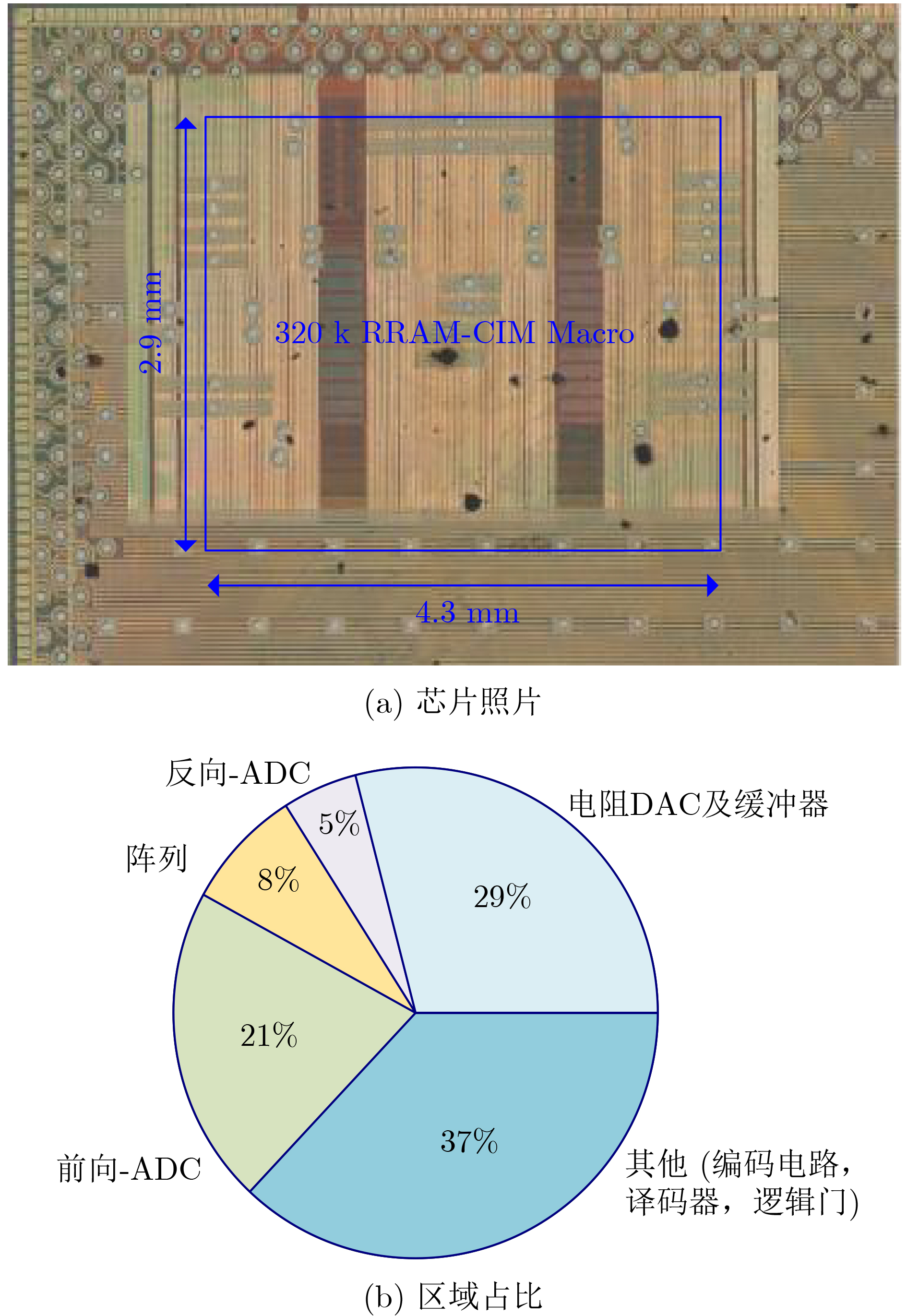
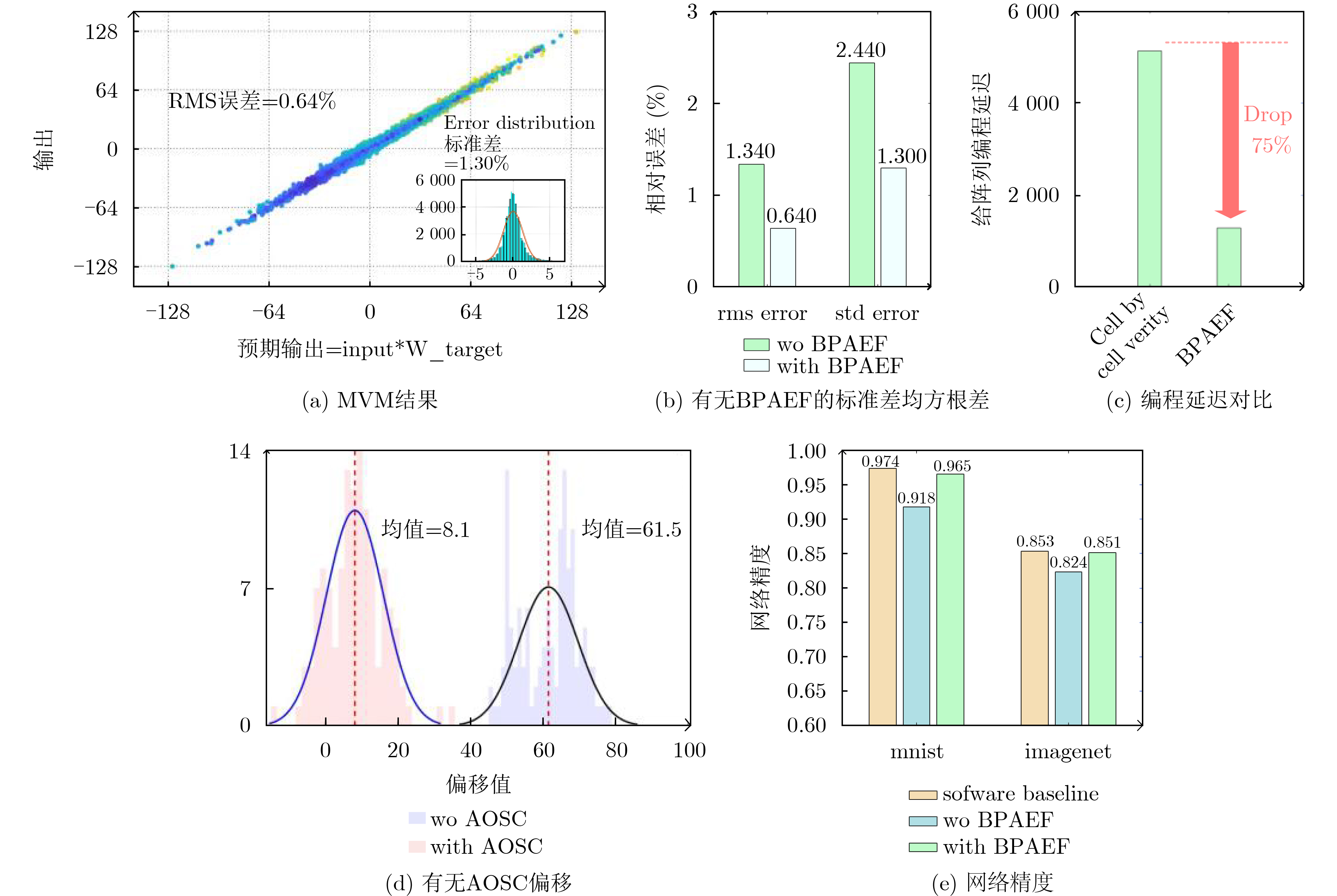
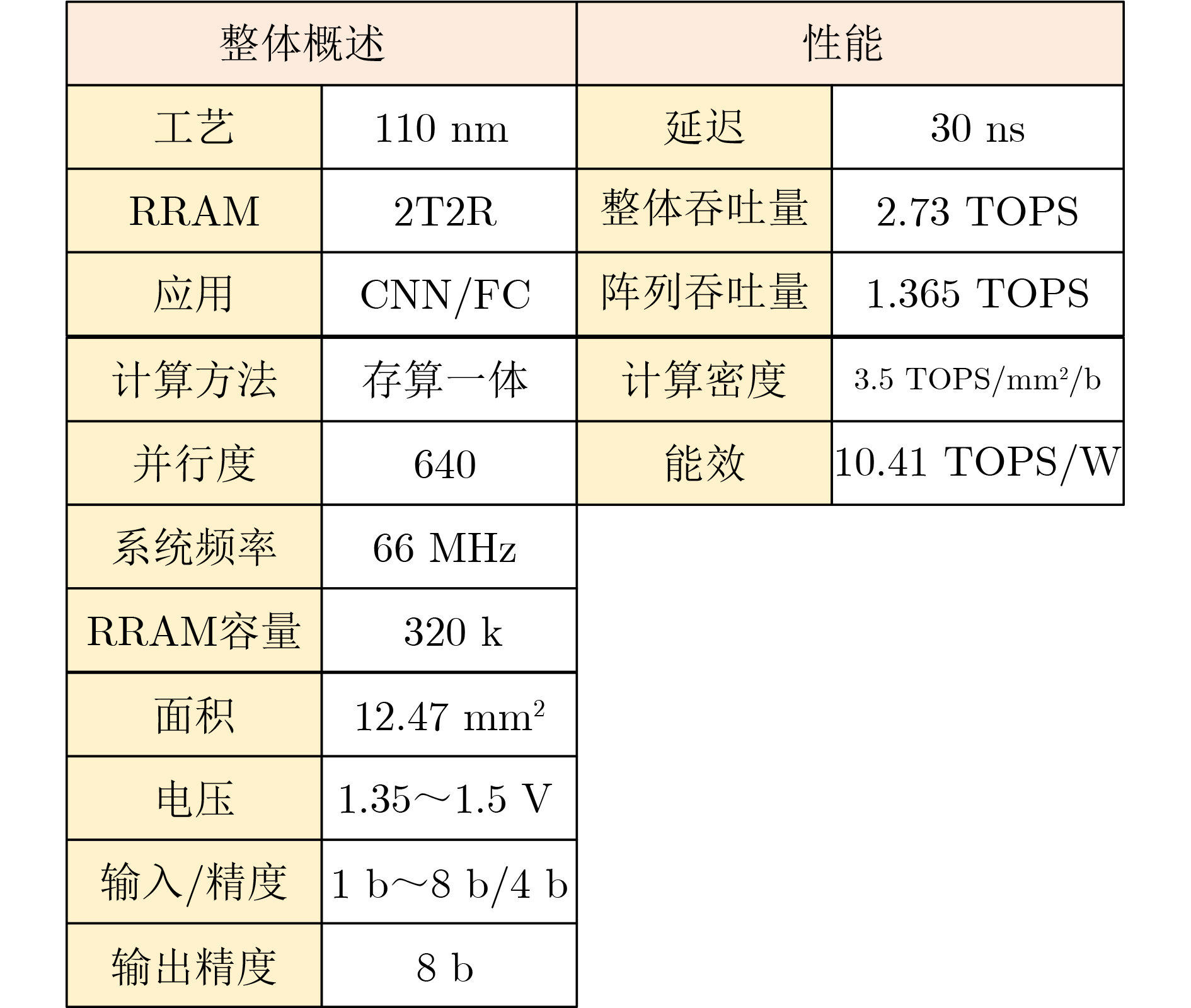
摘要: 推理大模型等人工智能的发展需要高能效、高算力芯片阻变随机存取存储器(RRAM)存算一体技术可以克服传统架构的“存储墙”瓶颈,大幅降低数据搬移的开销,实现高速、低功耗智能计算。当前,RRAM存算一体技术缺乏适配计算的高速、高精度编程方法,传统编程策略面临单器件校验耗时长以及电路非理想因素带来的精度损失挑战。为了提升RRAM高并行度模拟存算一体(CIM)的编程速度并提高权重编程精度,本文提出一种新型系统化编程策略:利用双向矩阵向量乘法(MVM)检测映射故障,并引入基于权重冗余行的原位偏移补偿方案,以高效校准不同通道的偏移。基于上述策略,制备了包含640×256子阵列与双通道ADC的RRAM存算一体芯片。在4位输入、4位权重、8位输出的配置下,该宏单元实现了编程延迟降低4倍,且在全并行MVM计算中取得0.64%的最低均方根(RMS)误差,提出的编程方法在图像识别任务中将识别准确率分别提升了4.7%和4.8%。Abstract:
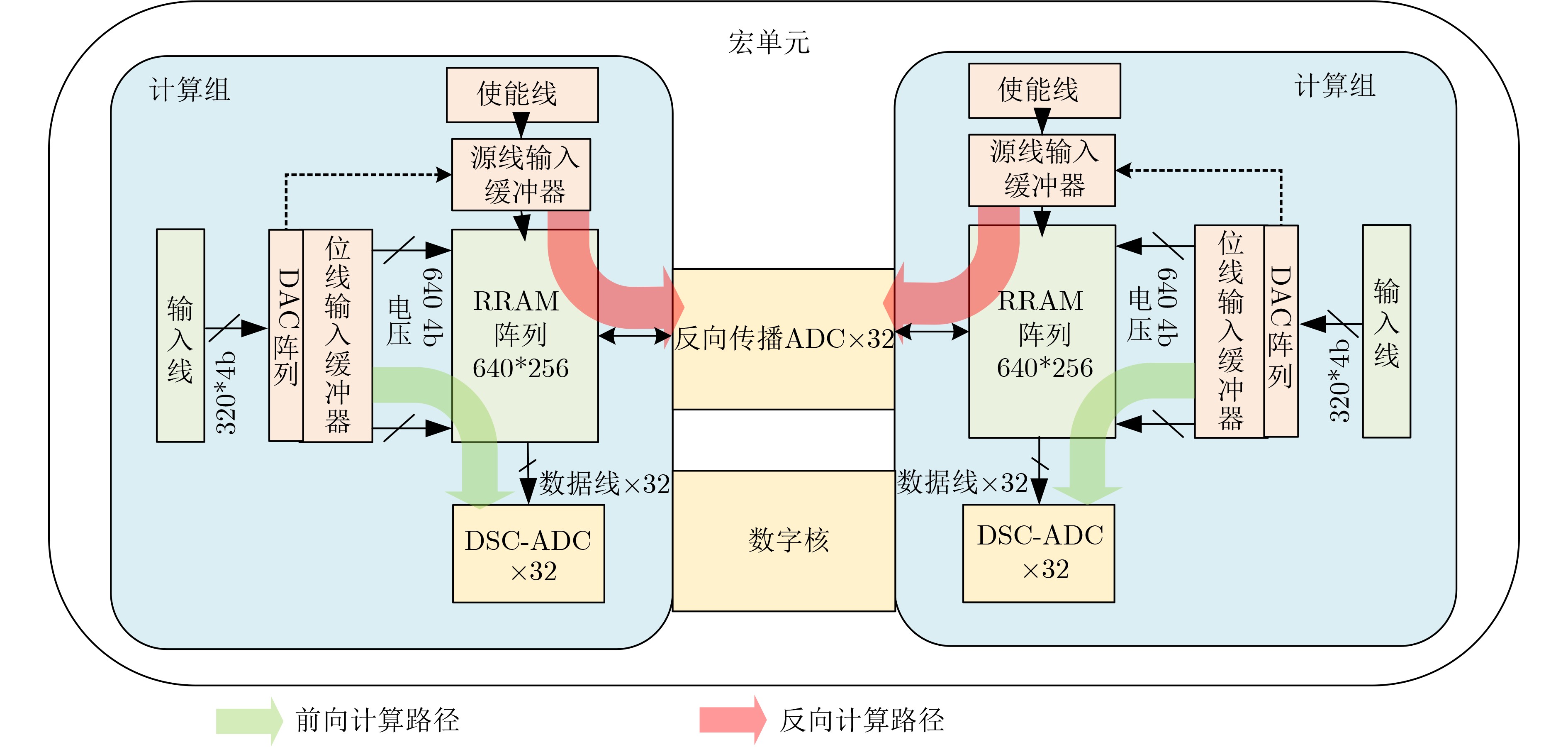
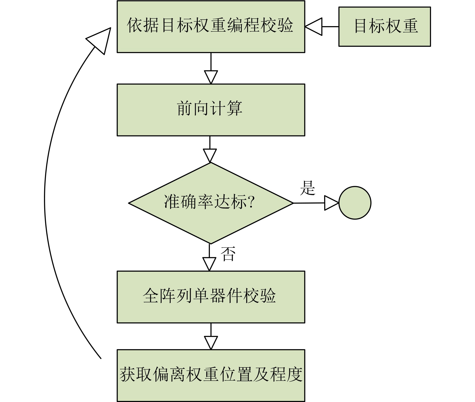
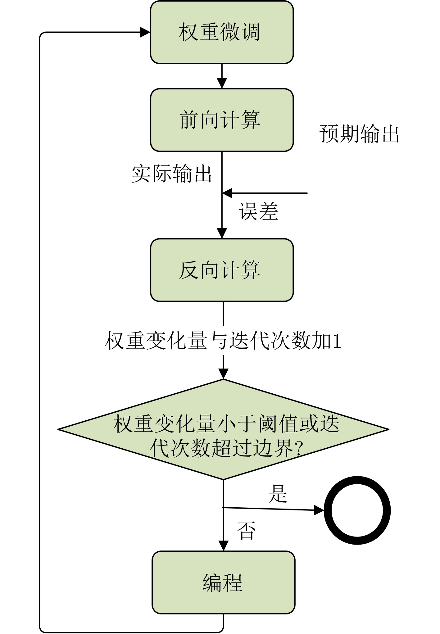
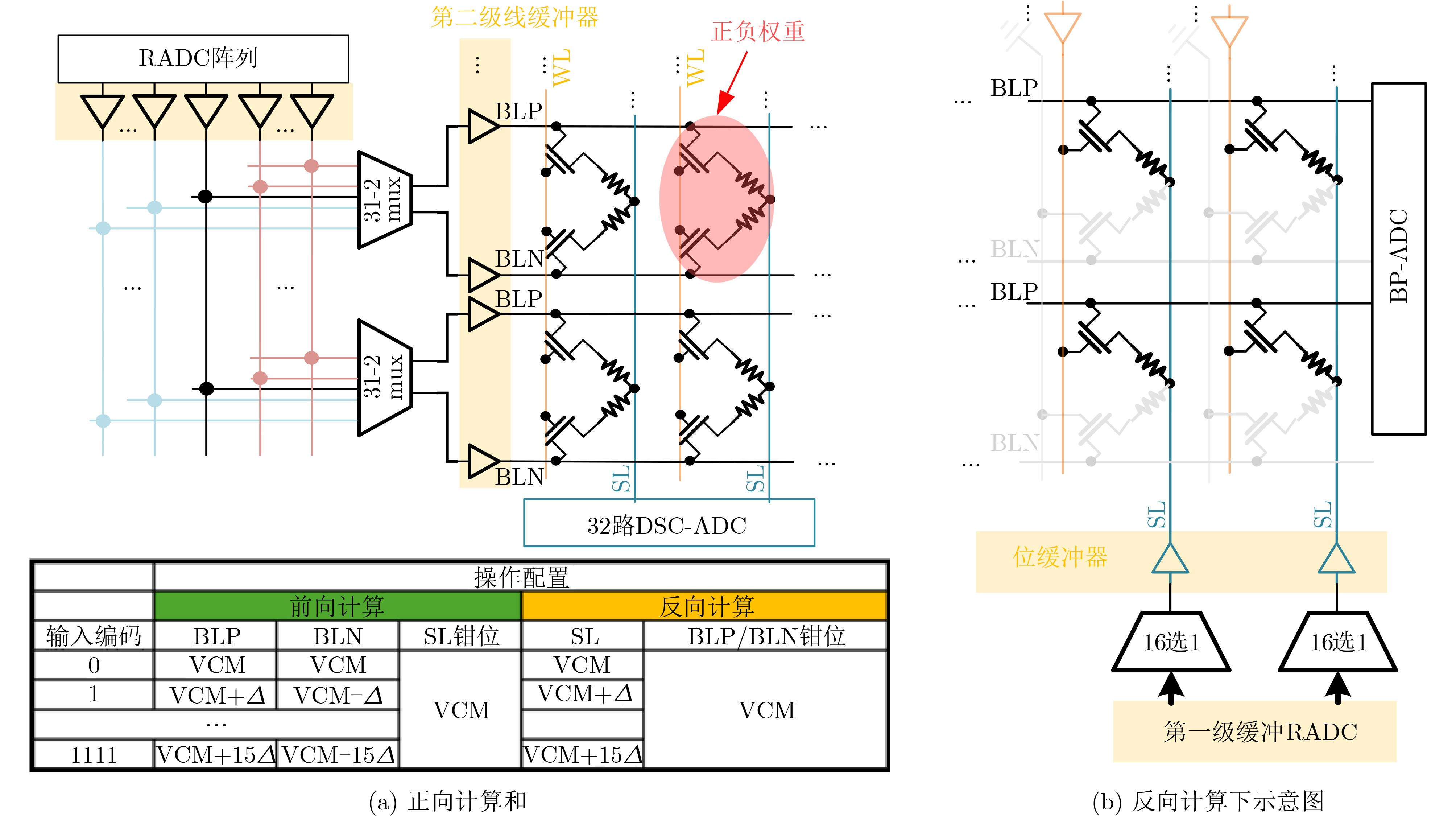
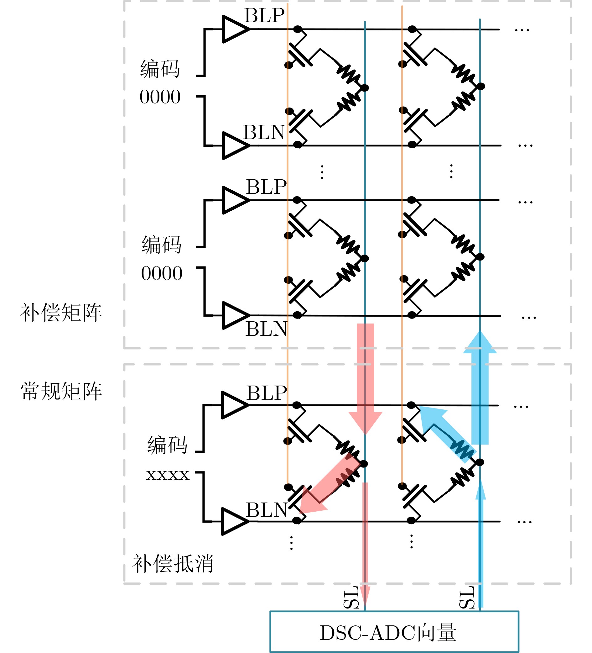
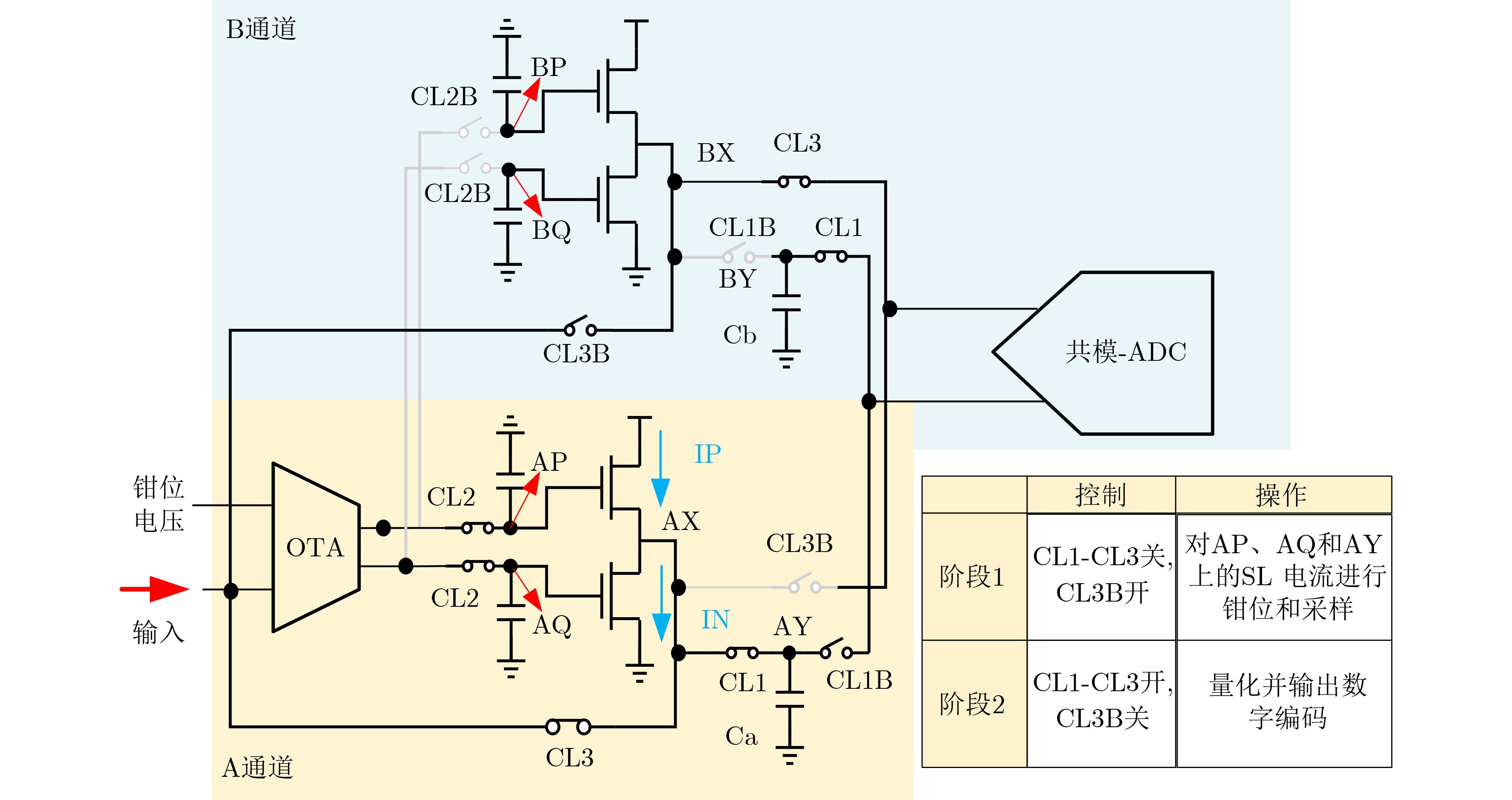
Objective Non-Volatile Memory (NVM)-based Compute-in-Memory (CIM) is considered a promising candidate for next-generation artificial intelligence accelerators because of its high energy efficiency and instant wake-up capability. However, the conventional Write-and-Verify (W&V) scheme cannot satisfy the speed and precision requirements of highly parallel CIM macros. The main limitation arises from the inefficient verification stage. Cell-by-cell reading must be repeated for the entire array, which significantly increases programming time. In addition, switching from the verify state, where only one row is active, to the compute state, where all rows are active, introduces systematic errors such as reference drift and IR-drop-induced weight inaccuracy. Analog CIM macros with on-chip programming must also tolerate large and non-uniform offsets under massive parallel operation. This work proposes three techniques: (1) a Back-Propagation-Assisted Programming (BPAP) scheme that rapidly and accurately locates failing cells without full-array verification; (2) an Analog-domain Offset-Canceling Structure (AOSC) that compensates channel-wise offsets in situ; and (3) a transposable Resistive Random-Access Memory (RRAM) macro equipped with parallel Two-Channel current-domain Analog-to-Digital Converters (TC-ADC), which doubles the effective sampling rate with only 15% additional ADC area. Methods As shown in Fig. 2 , the transposable RRAM macro contains two processing elements (PEs) and a shared backward-processing ADC (BP-ADC). Each PE includes an input loader (IL), a Digital-to-Analog Converter (DAC) array, a Bit-Line (BL) buffer and switch array, and 32 TC-ADCs. This configuration supports fully parallel forward computation. An Error Loader (EL) and a Source-Line (SL) buffer are also included to provide an error input vector for transposed matrix-vector multiplication (MVM).Fig. 3 illustrates the programming flow of the BPAP scheme. After AOSC calibration, a forward calculation is first executed. The differences between the expected outputs (yexp) and the measured outputs (yreal) are then computed on chip and used as inputs for the following back-propagation phase. The derivatives of the RRAM weights are calculated using several validation patterns. This training-like process adapts to the actual RRAM states and detects programming failures under the highly parallel computing condition. Weights with derivatives exceeding a predefined error threshold are selected for remapping. This approach enables accurate programming without performing cell-by-cell verification across the entire array. In the forward phase (Fig. 4a ), each 2T2R cell is configured as a signed weight, and the SLs are clamped at VCM by the TC-ADCs. For each PE, a fully parallel 4b-IN/4b-W MVM operation is completed with 320 active rows of 2T2R cells, and 32 ADCs perform simultaneous conversions. In the backward phase (Fig. 4b ), only the upper half of the reference voltages drives the SL buffers, and the weight is configured in 1T1R mode. Differential computation between the positive and negative 1T1R cells is performed by an external processor. Fig. 5 shows the operation of the AOSC scheme. Redundant rows in the RRAM array are programmed to compensate the analog computing offsets in situ. Offset currents are first measured by applying an all-zero input pattern to the regular weights. The redundant RRAM weights are then programmed to minimize the offset currents under a constant input voltage. During normal computation, these programmed redundancy rows receive the same input voltage to cancel the offsets. The macro supports this AOSC operation with only about 1% additional array area.Fig. 6 shows the TC-ADC architecture. A class-AB output stage, together with associated switches and capacitors, enables two-channel conversion and reduces the computation latency by half. This design increases the ADC area by only about 15% while achieving a 2× sampling rate.Conclusions Replacing the conventional W&V procedure with BPAP, together with AOSC calibration and TC-ADC acceleration, enables reliable and high-precision programming of analog RRAM-CIM macros under massive parallel operation. The measured results show 96.5% classification accuracy on MNIST and a 4.8% improvement on ImageNet. The proposed techniques are compatible with standard 2T2R and 1T1R RRAM bit cells and can be extended to larger arrays and deeper neural networks. -
表 1 与同类项目的对比
方法 本项目 VLSI[15] ISSCC 2022[16] ISSCC 2023[17] 工艺(nm) 110 14 22 22 年份 2024 2021 2022 2023 计算域 电流 电流 电荷 电流 支持反向传播 是 否 否 否 存算器件 模拟RRAM 模拟PCM SLC-PCM SLC/MLC RRAM 输入 4位电压 串行脉冲 位串行 位串行 并行度 640 256 8 16~128 输入 / 权重精度 4/8 8 8 4/8 电源电压 1.5 0.8 0.8 0.7~0.8 阵列吞吐量(TOPS) 1.365 | 0.341 1.008 0.004 0.843 | 0.257 阵列容量(K) 160(640×256) 252(256× 1024 )256( 1024 ×256)1024 (1024 ×1024 )能效(TOPS / W) 10.410 | 2.603 2.480 21.600 241.800 | 67.200 标准偏差 标准偏差:1.16%σ 标准偏差:1.94%σ 均方根误差 均方根误差:0.59% 均方根误差:1%~2%  下载: 导出CSV
-
[1] XU Xiaowei, DING Yukun, HU S X, et al. Scaling for edge inference of deep neural networks[J]. Nature Electronics, 2018, 1(4): 216–222. doi: 10.1038/s41928-018-0059-3. [2] RADFORD A, WU J, CHILD R, et al. Language models are unsupervised multitask learners[J/OL]. Computer Science, Linguistics, 2019. [3] KRIZHEVSKY A, SUTSKEVER I, and HINTON G E. ImageNet classification with deep convolutional neural networks [J]. Communications of the ACM, 2017, 60 (6):84–90. [4] FUJIWARA H, MORI H, ZHAO Weichang, et al. A 3nm, 32.5TOPS/W, 55.0TOPS/mm2 and 3.78Mb/mm2 fully-digital compute-in-memory macro supporting INT12 × INT12 with a parallel-MAC architecture and foundry 6T-SRAM bit cell[C]. 2024 IEEE International Solid-State Circuits Conference, San Francisco, USA, 2024: 572–573. doi: 10.1109/ISSCC49657.2024.10454556. [5] GHOLAMI A, YAO Zhewei, KIM S, et al. AI and memory wall[J]. IEEE Micro, 2024, 44(3): 33–39. doi: 10.1109/MM.2024.3373763. [6] BÜCHEL J, VASILOPOULOS A, KERSTING B, et al. Gradient descent-based programming of analog in-memory computing cores[C]. 2022 International Electron Devices Meeting, San Francisco, USA, 2022: 779–782. doi: 10.1109/IEDM45625.2022.10019486. [7] JACOB B, KLIGYS S, CHEN Bo, et al. Quantization and training of neural networks for efficient integer-arithmetic-only inference[EB/OL]. https://doi.org/10.48550/arXiv.1712.05877, 2017. [8] RADHAKRISHNAN J, BELMONTE A, CLIMA S, et al. Improving post-cycling low resistance state retention in resistive RAM with combined oxygen vacancy and copper filament[J]. IEEE Electron Device Letters, 2019, 40(7): 1072–1075. doi: 10.1109/LED.2019.2917553. [9] SHIM W, MENG Jian, PENG Xiaochen, et al. Impact of multilevel retention characteristics on RRAM based DNN inference engine[C]. Proceedings of 2021 IEEE International Reliability Physics Symposium, Monterey, USA, 2021: 1–4. doi: 10.1109/IRPS46558.2021.9405210. [10] CHIU Y C, KHWA W S, LI C Y, et al. A 22nm 8Mb STT-MRAM near-memory-computing macro with 8b-precision and 46.4–160.1TOPS/W for edge-AI devices[C]. Proceedings of 2023 IEEE International Solid-State Circuits Conference, San Francisco, USA, 2023: 496–497. doi: 10.1109/ISSCC42615.2023.10067563. [11] YOU Deqi, KHWA W S, WU J J, et al. A 22nm nonvolatile AI-edge processor with 21.4TFLOPS/W using 47.25Mb lossless-compressed-computing STT-MRAM near-memory-compute macro[C]. 2024 IEEE Symposium on VLSI Technology and Circuits, Honolulu, USA, 2024: 1–2. doi: 10.1109/VLSITechnologyandCir46783.2024.10631408. [12] WANG Yang, YANG Xiaolong, QIN Yubin, et al. A 28nm 83.23TFLOPS/W POSIT-based compute-in-memory macro for high-accuracy AI applications[C]. 2024 IEEE International Solid-State Circuits Conference, San Francisco, USA, 2024: 566–567. doi: 10.1109/ISSCC49657.2024.10454567. [13] KHWA W S, WU Pingchun, WU J J, et al. A 16nm 96Kb integer/floating-point dual-mode-gain-cell-computing-in-memory macro achieving 73.3–163.3TOPS/W and 33.2–91.2TFLOPS/W for AI edge-devices[C]. 2024 IEEE International Solid-State Circuits Conference, San Francisco, USA, 2024: 568–569. doi: 10.1109/ISSCC49657.2024.10454447. [14] MORI H, ZHAO Weichang, LEE C E, et al. A 4nm 6163-TOPS/W/b 4790-TOPS/mm2/b SRAM based digital-computing-in-memory macro supporting bit-width flexibility and simultaneous MAC and weight update[C]. 2023 IEEE International Solid-State Circuits Conference, San Francisco, USA, 2023: 132–133. doi: 10.1109/ISSCC42615.2023.10067555. [15] KHADDAM-ALJAMEH R, STANISAVLJEVIC M, FORNT MAS J, et al. HERMES core – A 14nm CMOS and PCM-based in-memory compute core using an array of 300ps/LSB linearized CCO-based ADCs and local digital processing[C]. 2021 Symposium on VLSI Circuits, Kyoto, Japan, 2021: 1–2. doi: 10.23919/VLSICircuits52068.2021.9492362. [16] HUNG J M, HUANG Y H, HUANG S P, et al. An 8-Mb DC-current-free binary-to-8b precision ReRAM nonvolatile computing-in-memory macro using time-space-readout with 1286.4–21.6TOPS/W for edge-AI devices[C]. 2022 IEEE International Solid-State Circuits Conference, San Francisco, USA, 2022: 1–3. doi: 10.1109/ISSCC42614.2022.9731715. [17] HUANG W H, WEN Taihao, HUNG J M, et al. A nonvolatile Al-edge processor with 4MB SLC-MLC hybrid-mode ReRAM compute-in-memory macro and 51.4–251TOPS/W[C]. 2023 IEEE International Solid-State Circuits Conference, San Francisco, USA, 2023: 15–17. doi: 10.1109/ISSCC42615.2023.10067610. -

 下载:
下载:


图(9) / 表(1)
计量
- 文章访问数: 1190
- HTML全文浏览量: 510
- PDF下载量: 188
- 被引次数: 0
