

A 64 Gb/s Single-Ended Simultaneous Bi-Directional Transceiver for Die-to-Die Interfaces
-
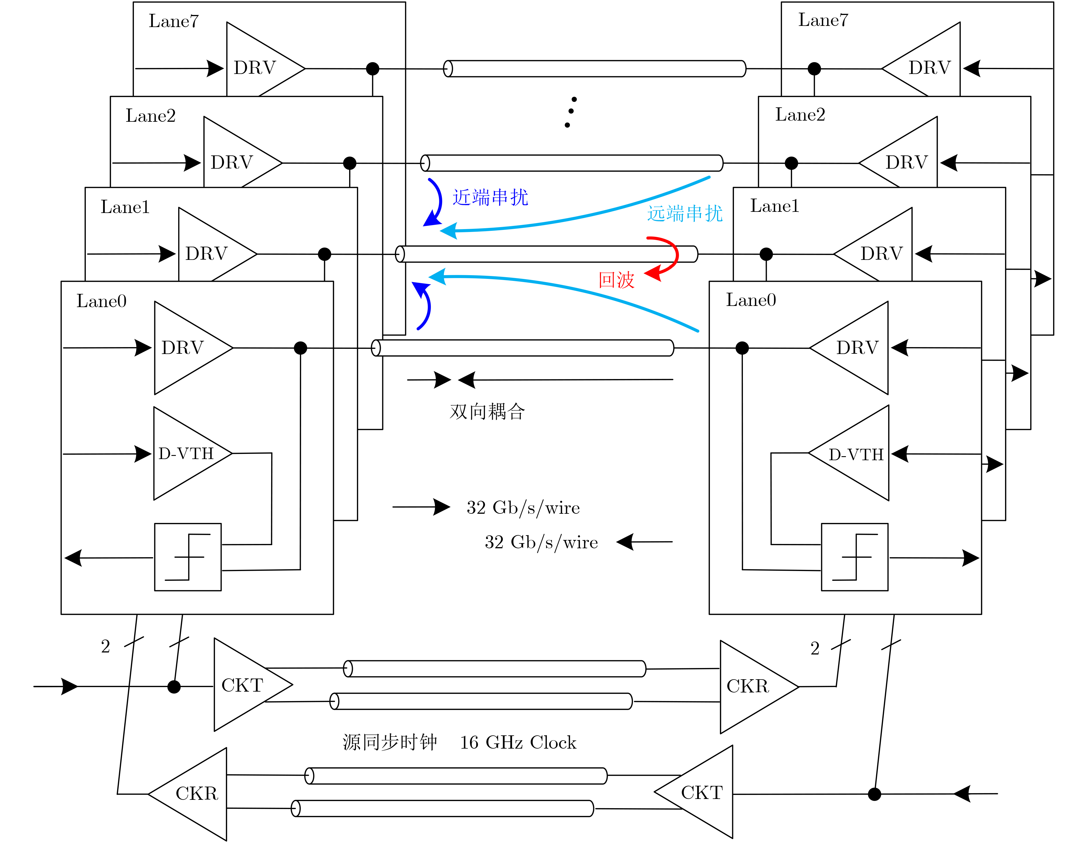
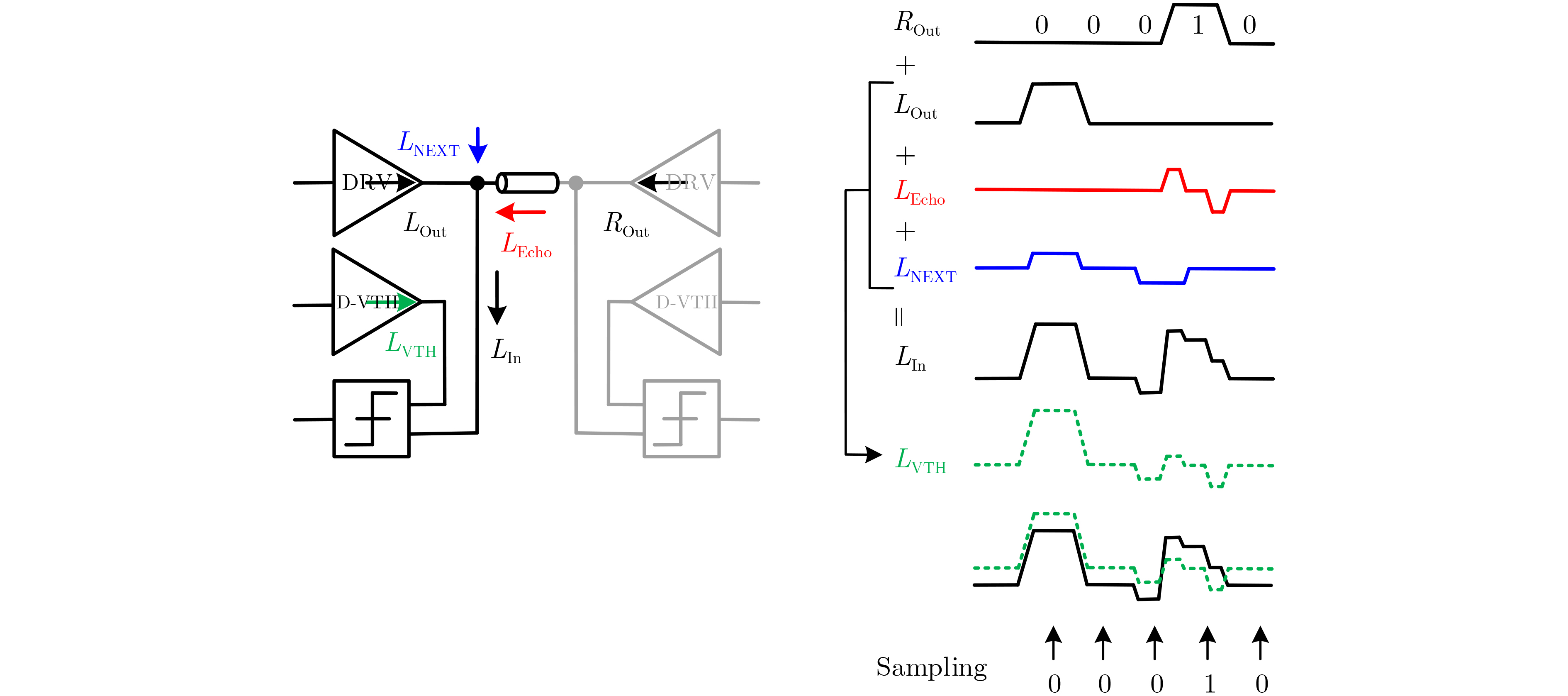
摘要: 芯粒集成将多颗不同功能、工艺的芯粒封装在一起,为高性能芯片发展开辟了新的思路。芯粒间互连接口电路作为数据传输的纽带,其带宽密度、误码率和功耗对芯片算力和数据吞吐量等关键性能至关重要。针对带宽密度提升带来的信号反射和串扰等问题,该文提出了一种具备回波、近端串扰和远端串扰消除功能的全双工收发机电路,并基于28 nm工艺进行了流片验证。其利用全双工技术提升了单通道数据速率,利用动态阈值判决技术实现了双向收发信号分离、回波与近端串扰消除,利用信道间容性与感性耦合的平衡实现了远端串扰消除。此外,延时匹配的源同步时钟结构降低了时钟相对数据抖动、提升了噪声容限,驻波与重置信号传输电路实现了发送信号的同步,提高了近端串扰消除精度。测试结果表明,在3 mm长的无屏蔽互连信道上,此收发机可以64 Gb/s的单通道速率、10.5 Tb/(s·mm)的带宽密度,实现低于10–16的误码率,能效为1.21 pJ/b。Abstract:
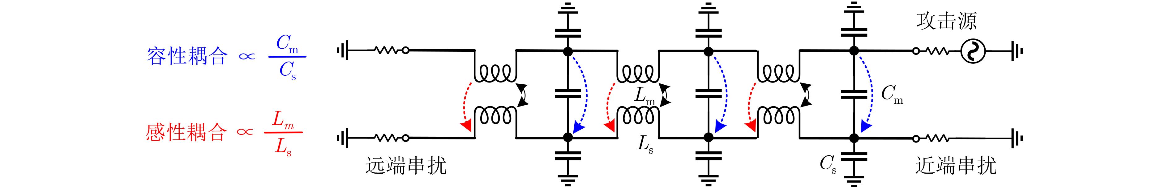
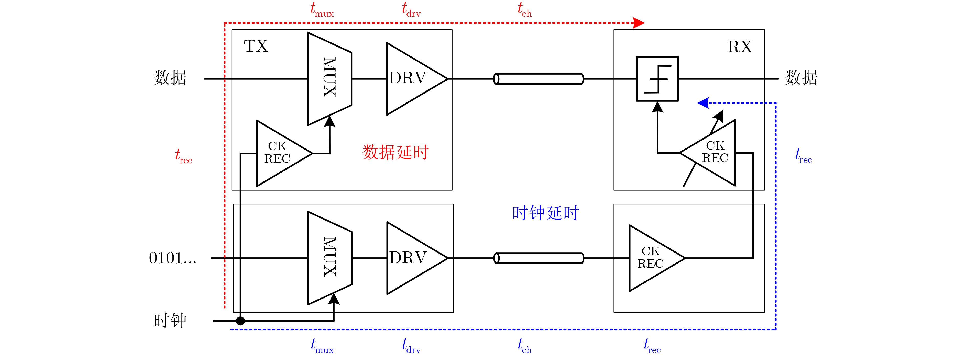
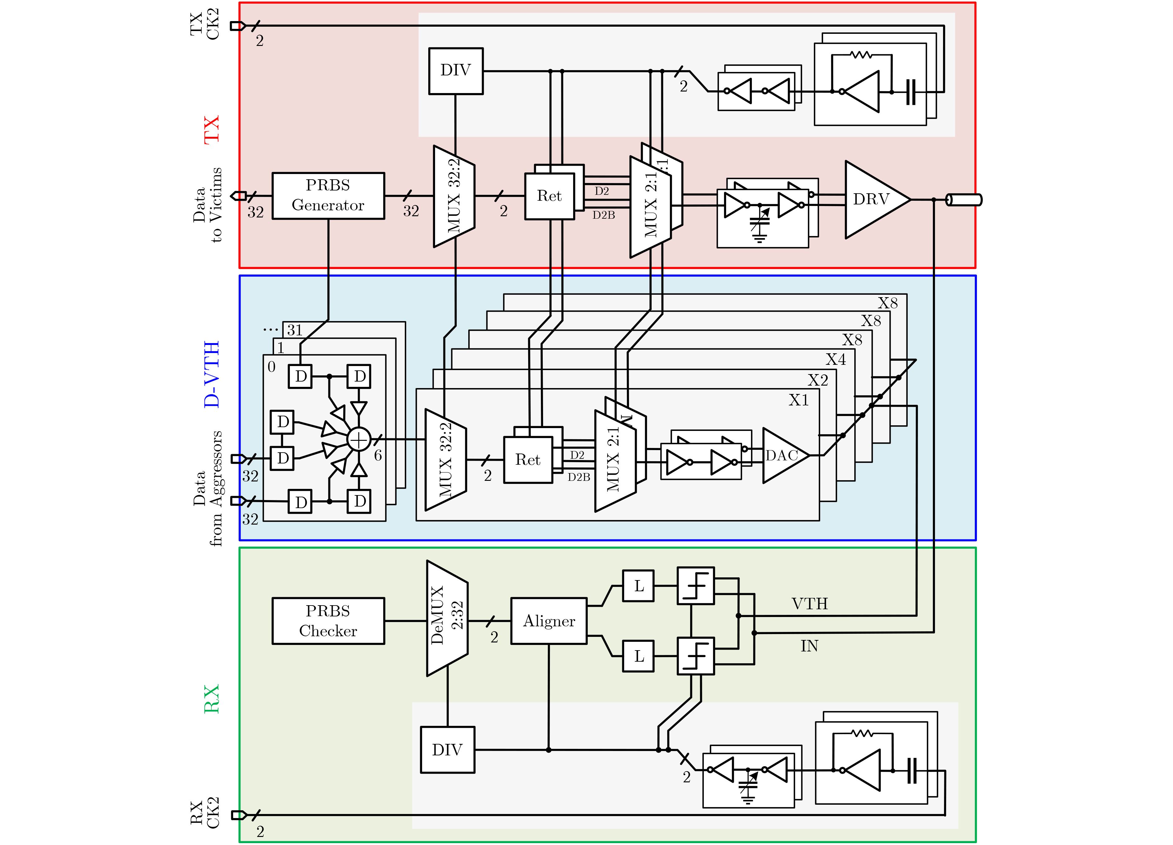
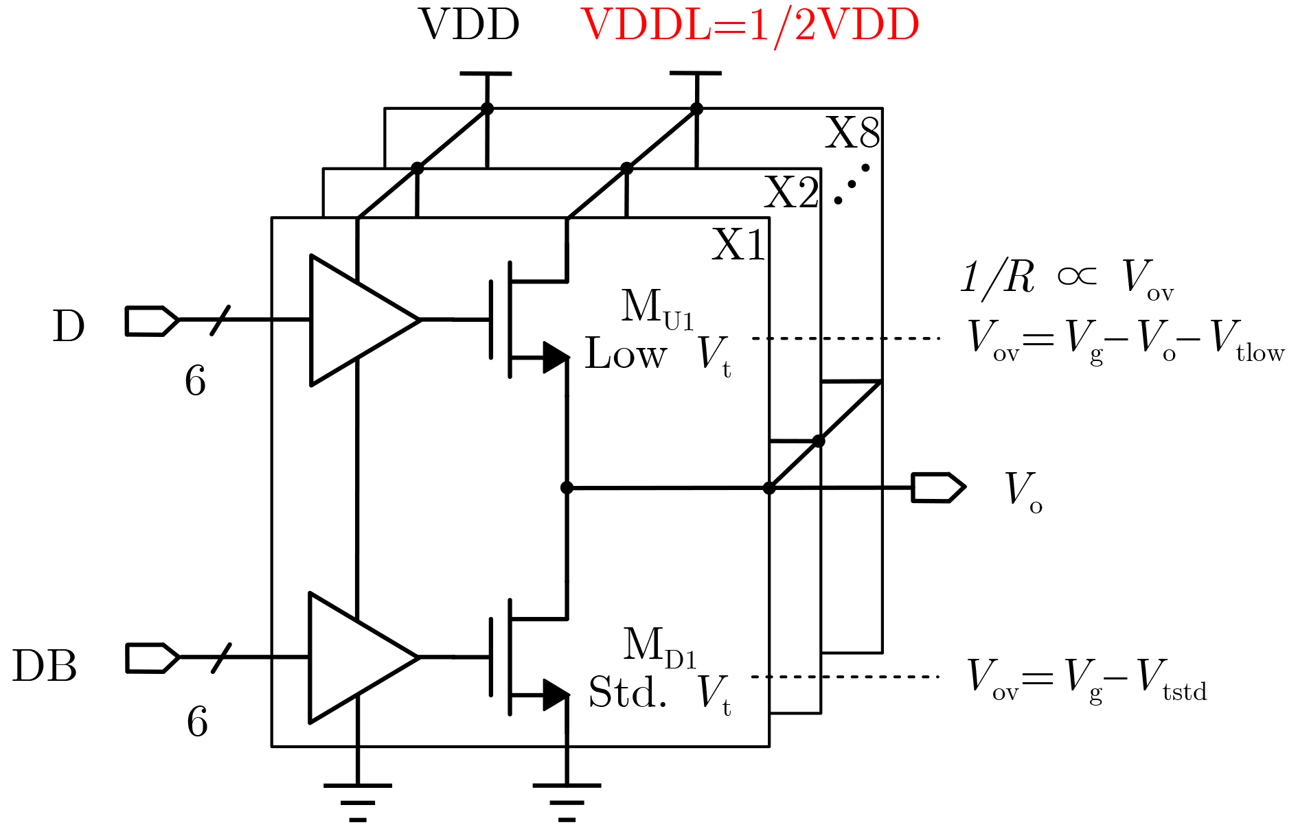
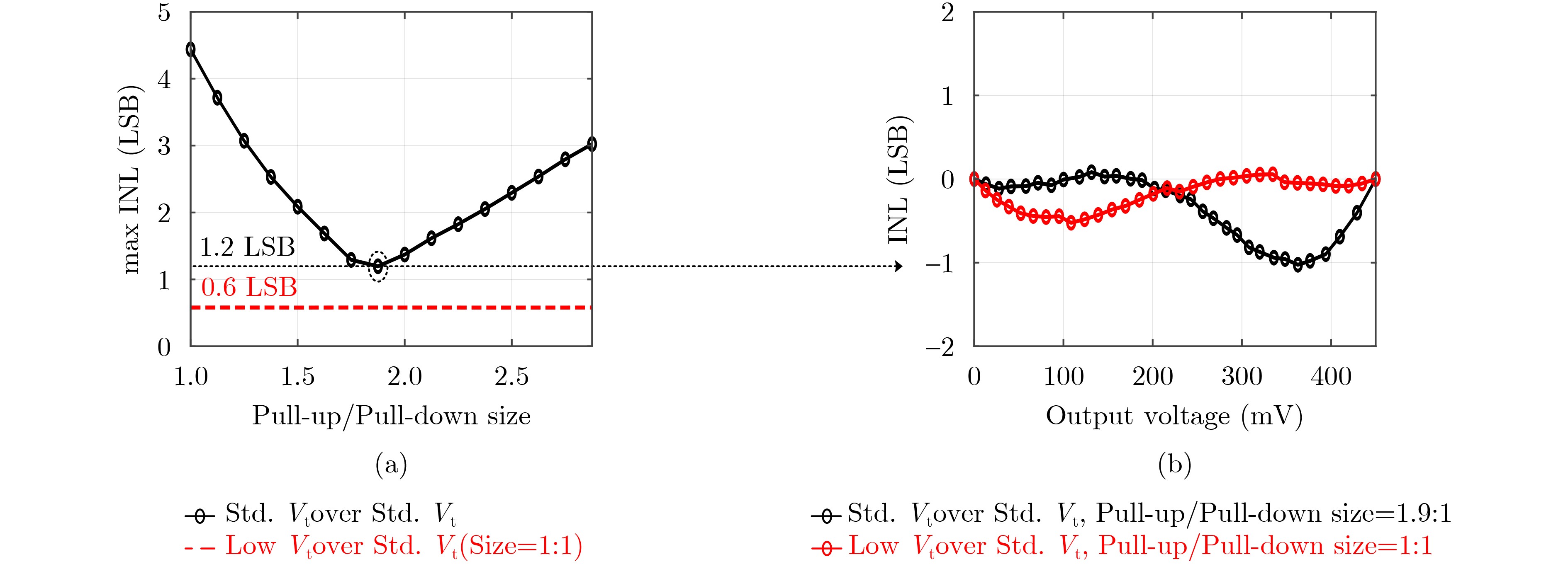
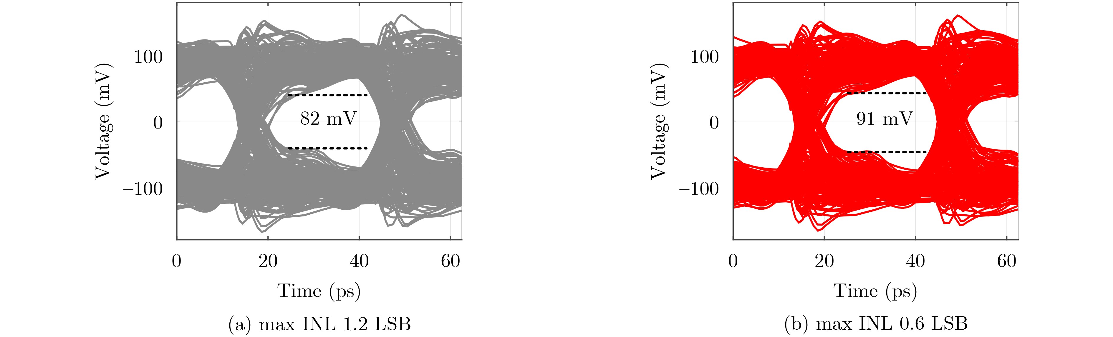
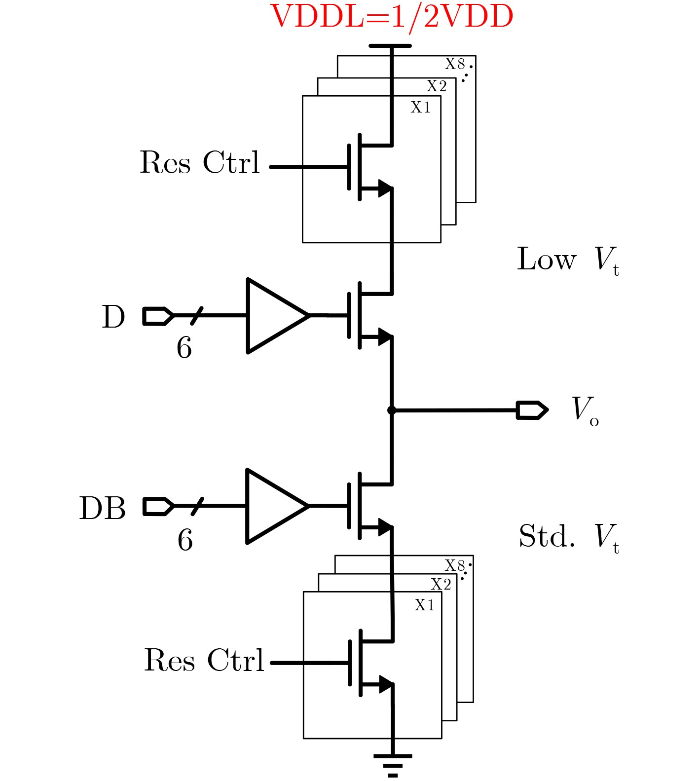
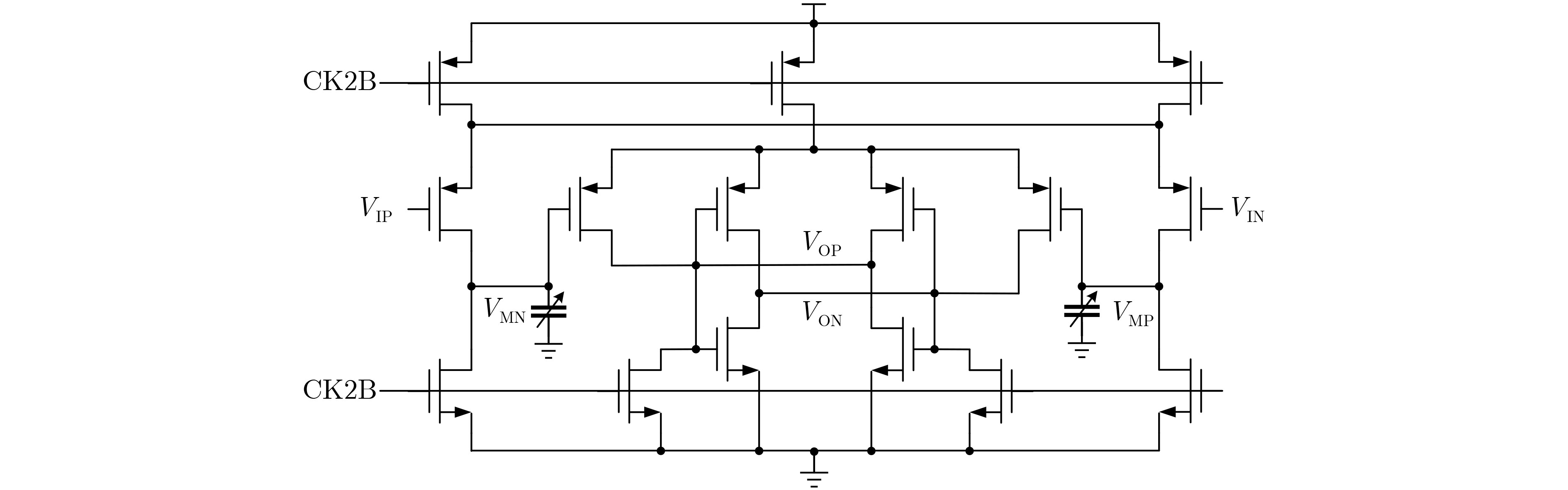
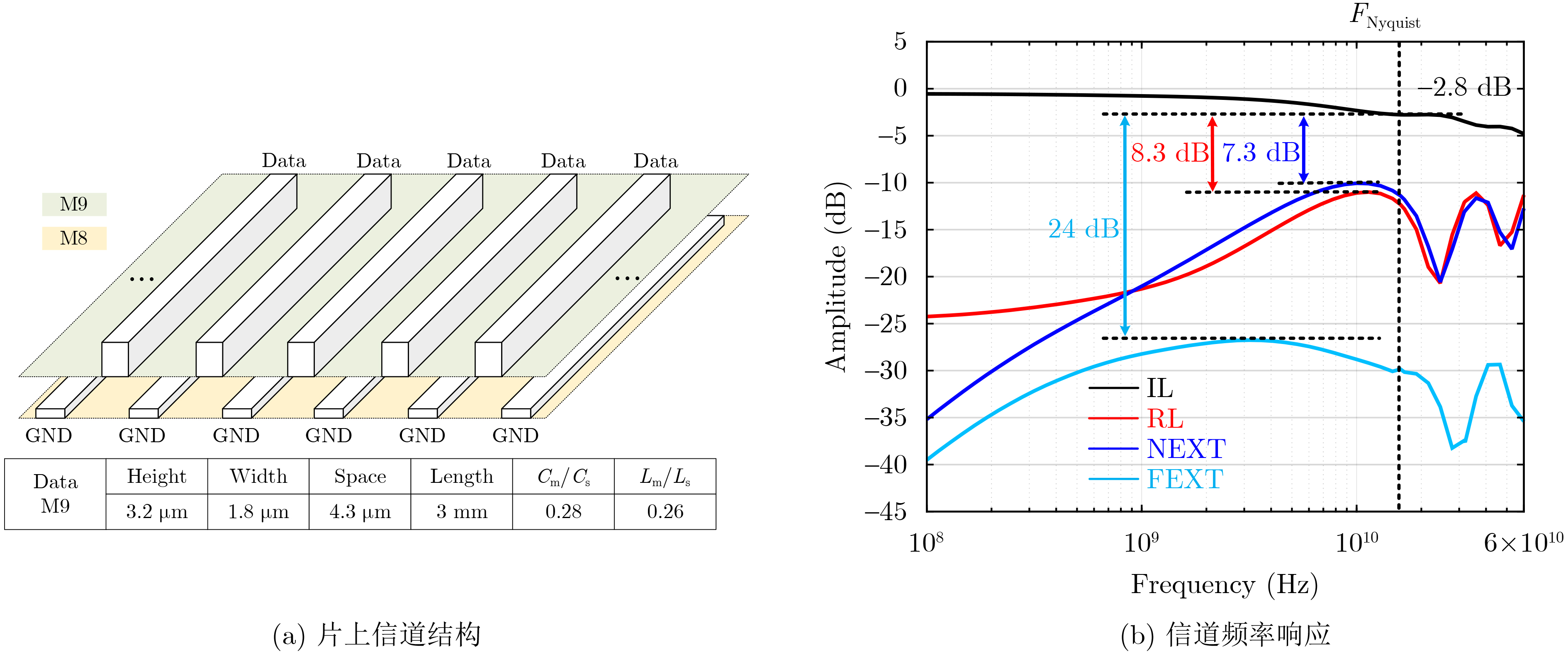
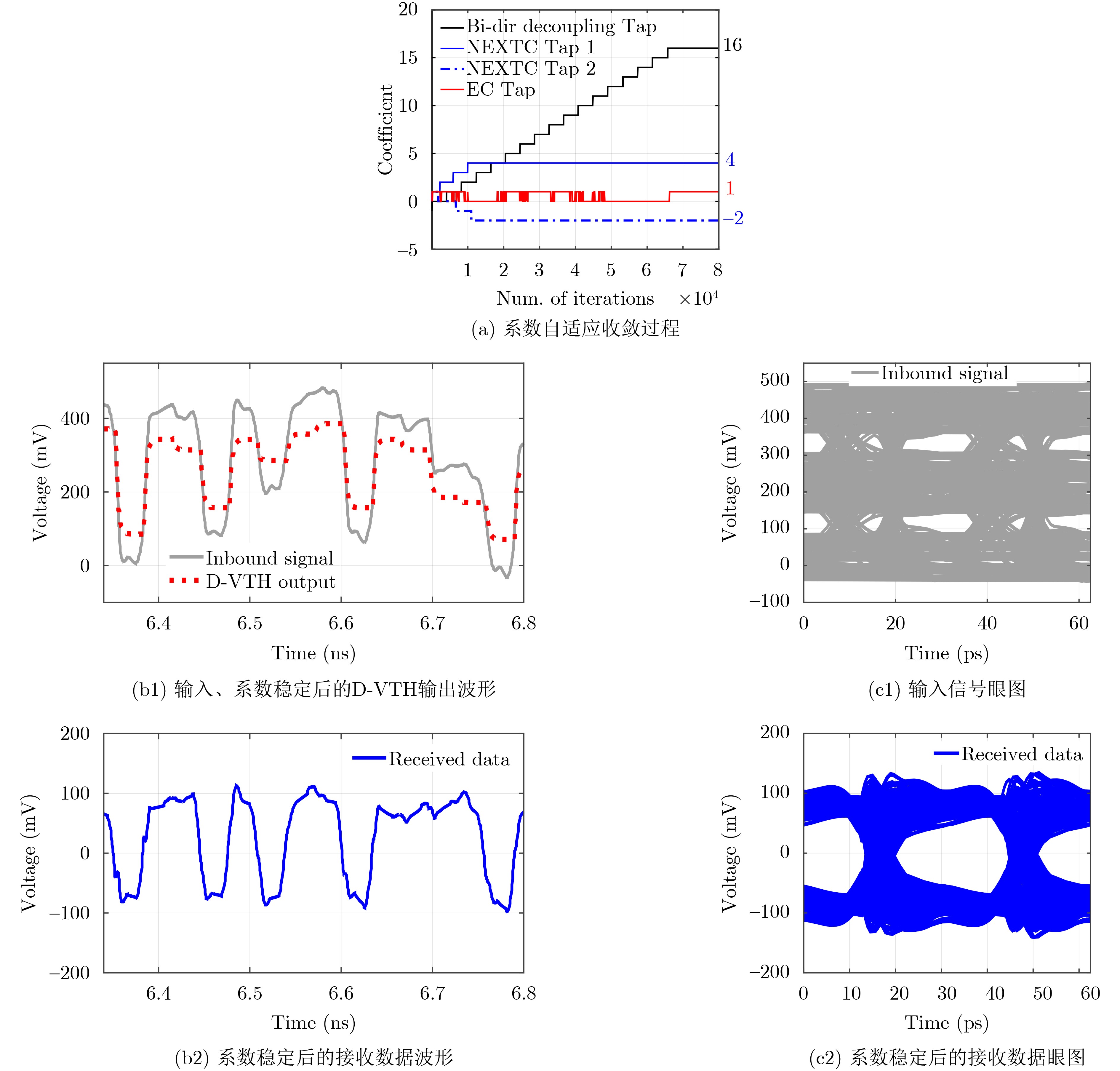
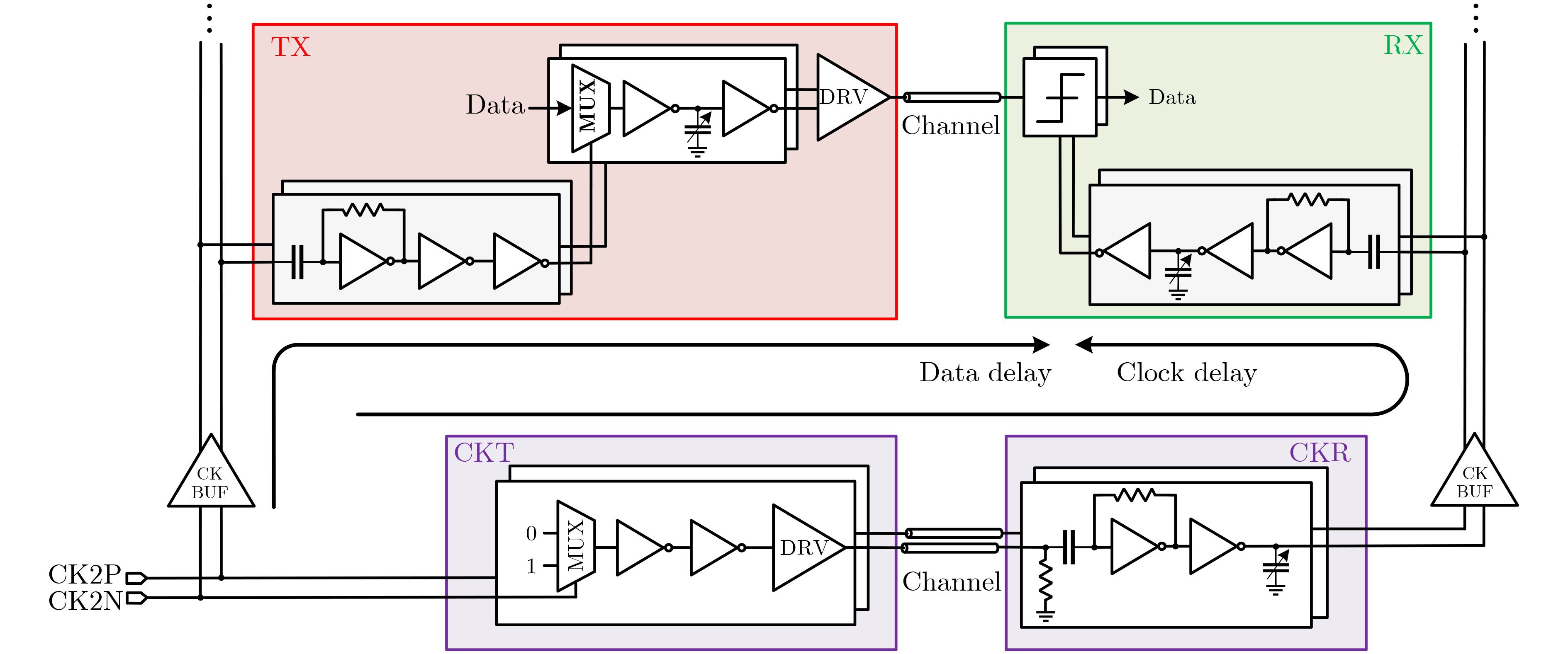
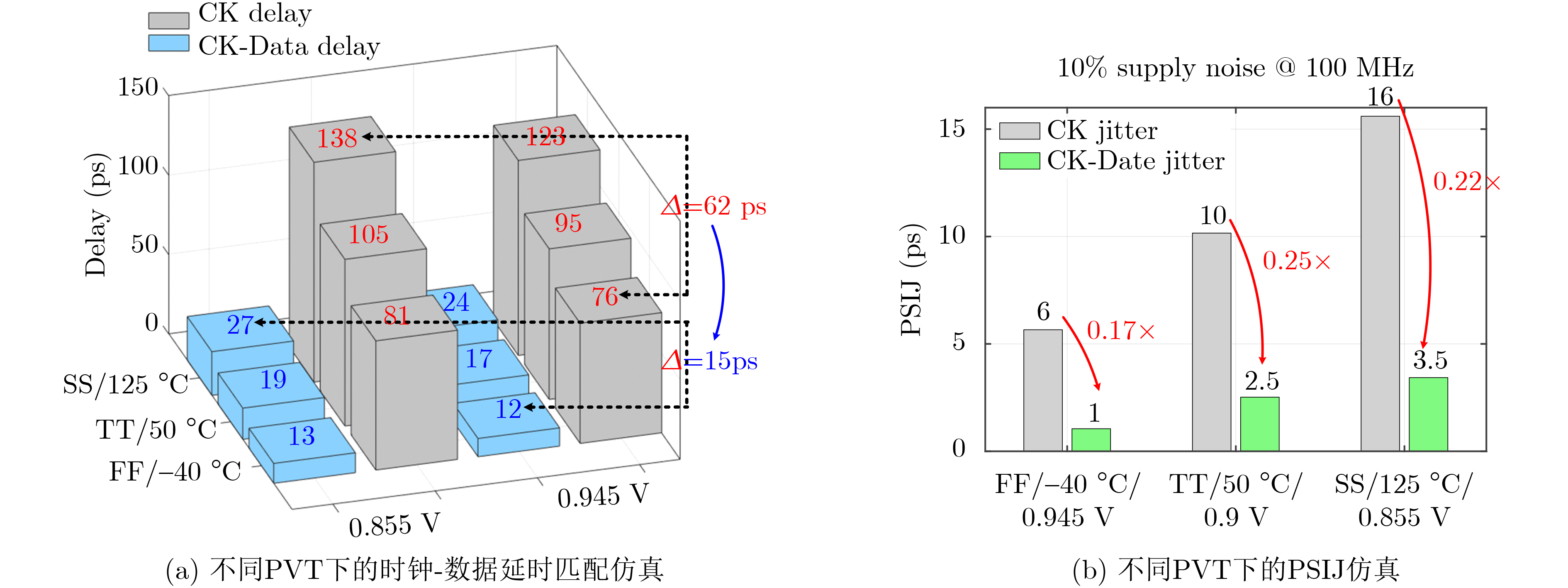
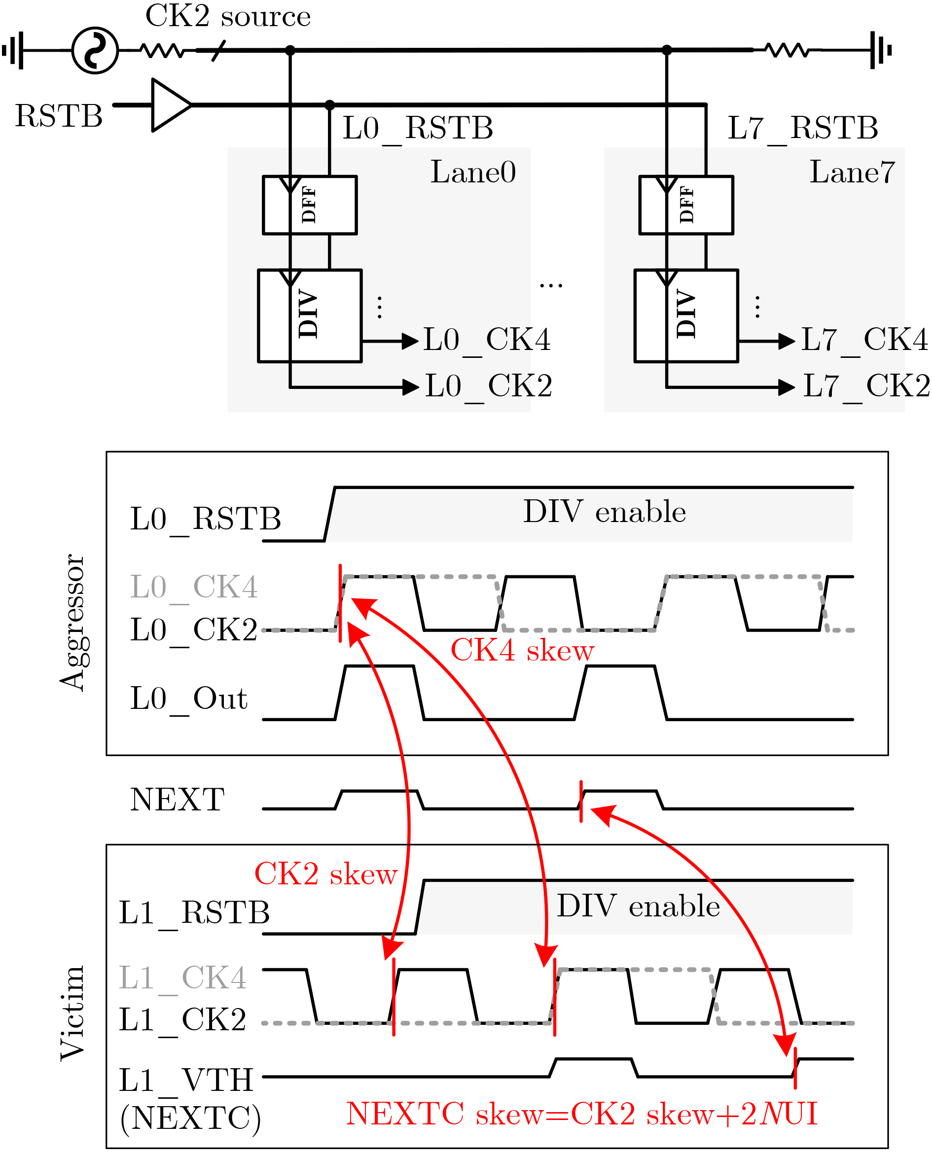
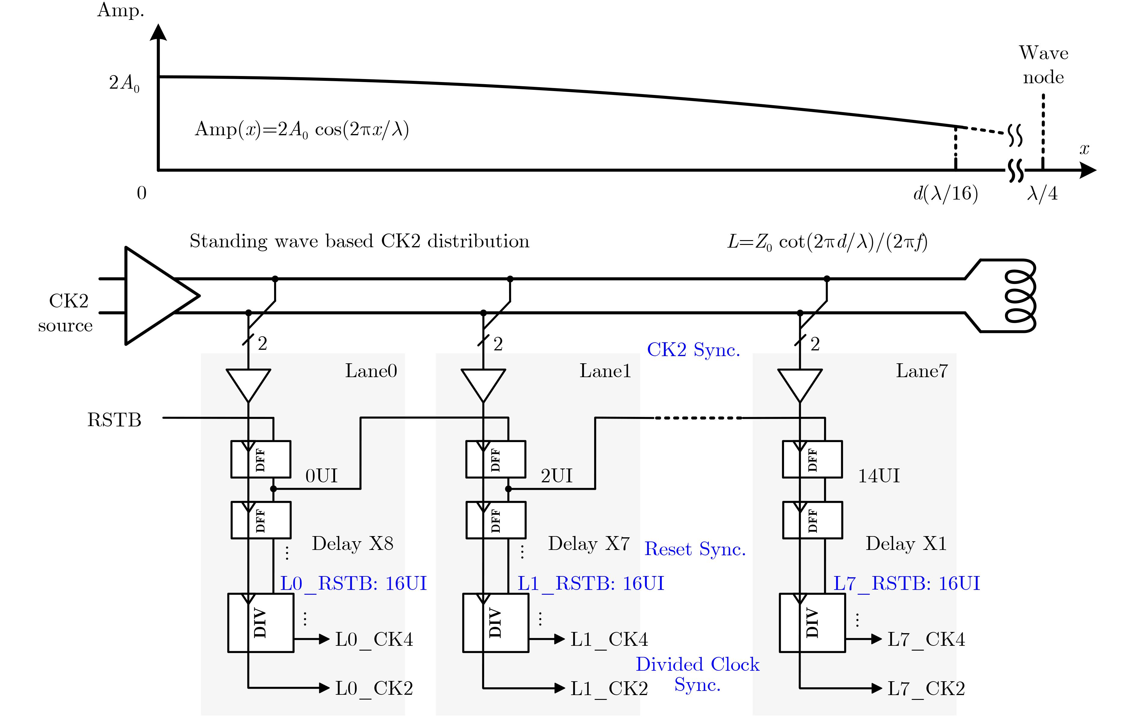
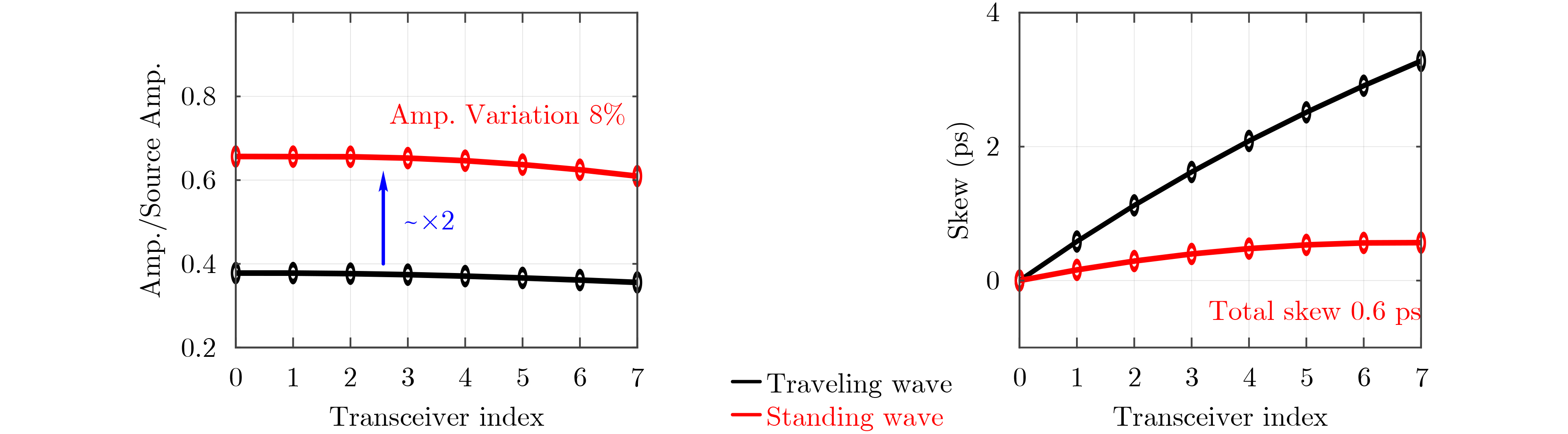
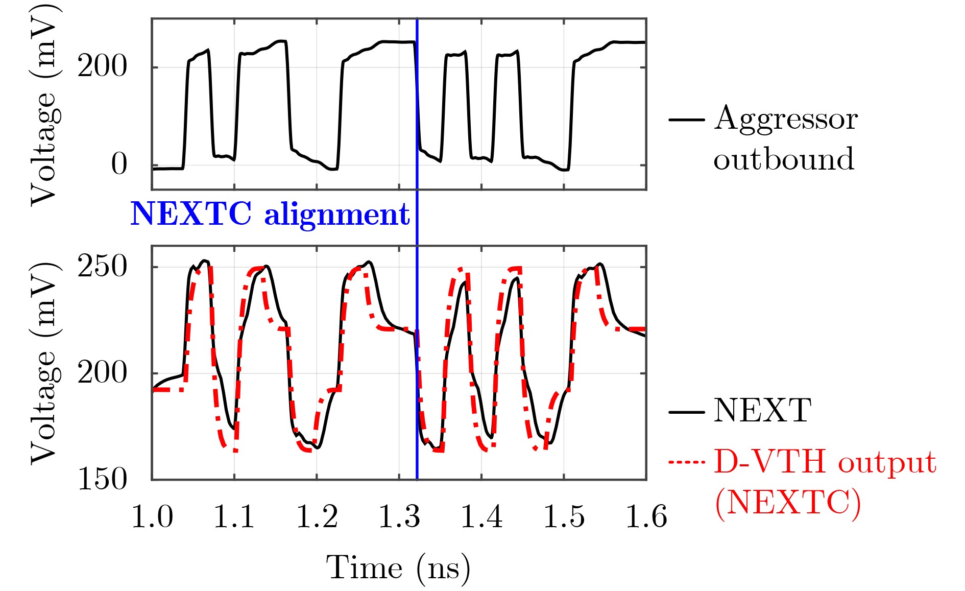
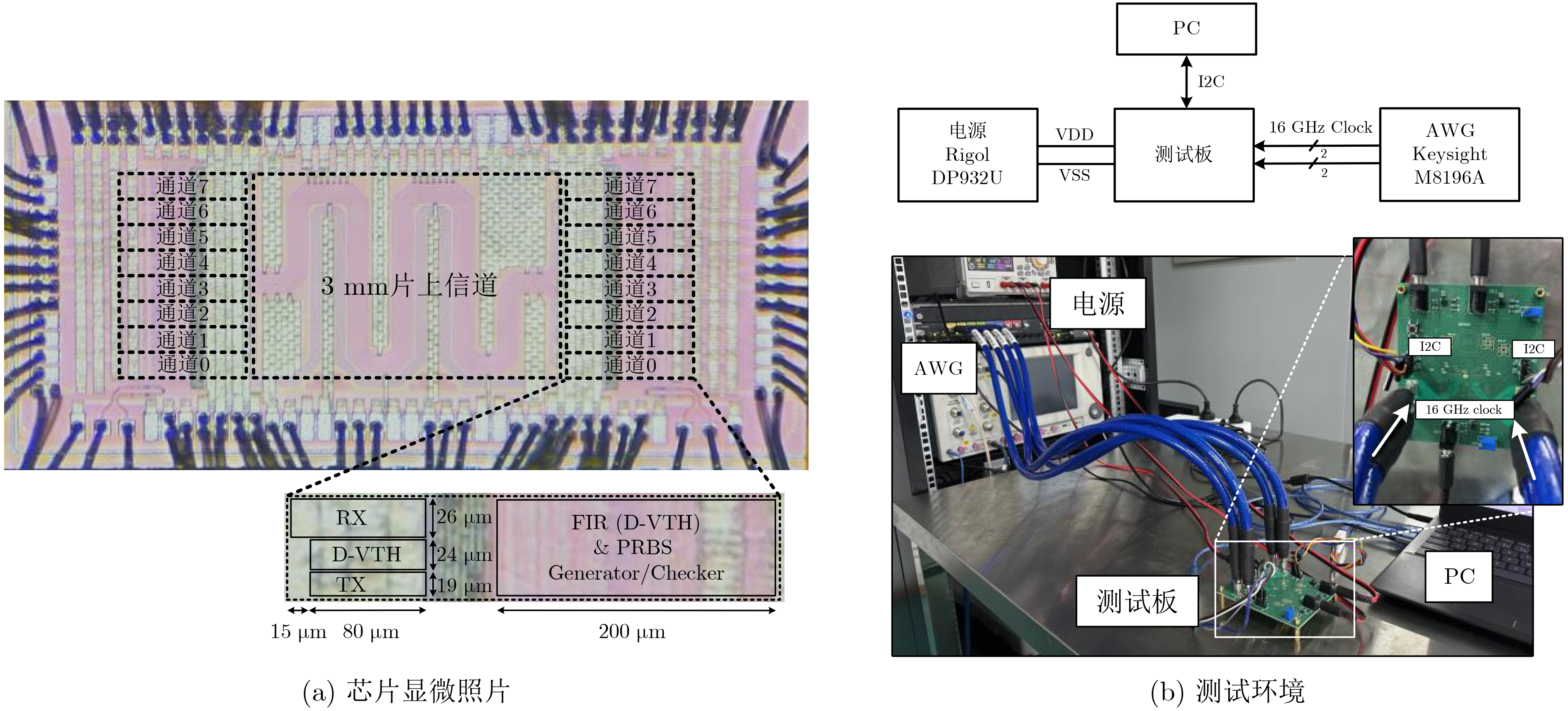
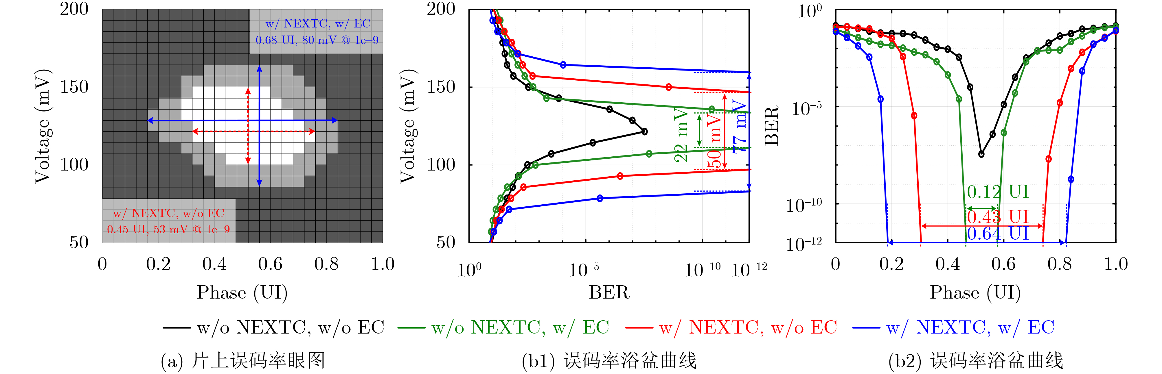
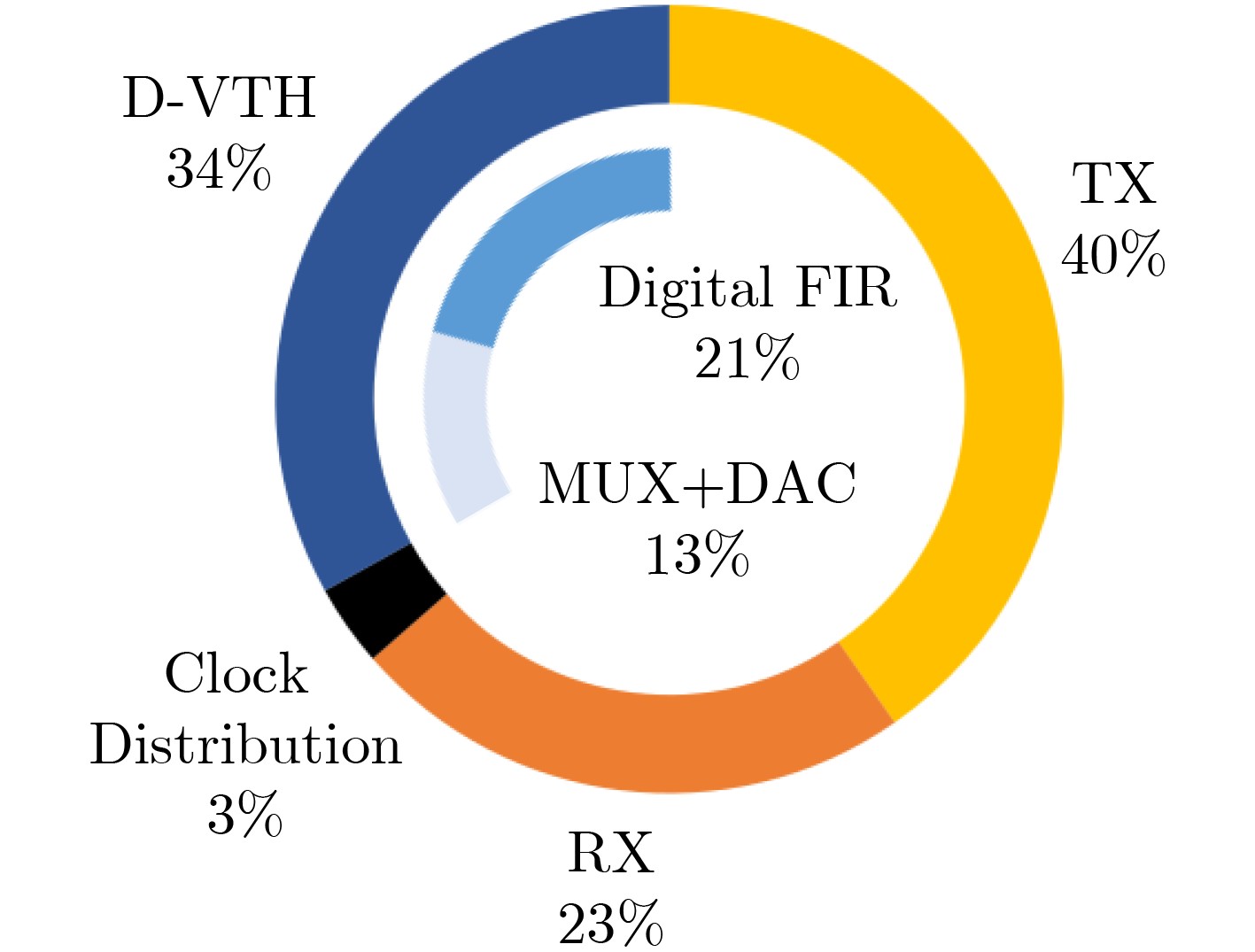
Objective Chiplet technology, which packages multiple dies with different functions and processes together, offers a cost-effective way for fabricating high-performance chips. For die-to-die data transmission, the edge density, Bit Error Rate (BER), and power consumption of the interface are crucial to the chip’s key performance metrics, such as computing power and throughput. Simultaneous Bi-Directional (SBD) signaling is an effective way to double the edge density by transmitting and receiving data on the same channel. However, with higher data rate and smaller channel pitch, channel reflection and crosstalk bring severe challenges to the design of interface circuits. This paper presents a single-ended SBD transceiver with echo and crosstalk cancellation to achieve a larger edge density and a lower BER. Methods The transceiver improves the per-wire data rate by utilizing the SBD signaling and denser shield-less channels. However, as both ends of the channel transmit data simultaneously, bi-directional signal coupling arises. Signal coupling, echo from impedance mismatch, and crosstalk from adjacent channels degrade the received data’s Signal-to-Noise Ratio (SNR). To decouple the bi-directional signal and cancel the echo and Near-End Crosstalk (NEXT), this paper proposes a Dynamic Voltage ThresHold generator (D-VTH). It generates the slicer’s threshold voltage according to the interfering signals needing to be subtracted. To cancel the Far-End Crosstalk (FEXT), a channel with the same capacitive and inductive coupling is designed by adjusting its width and space. FEXT is the subtraction of these two kinds of coupling, so it is canceled as expected. The source-synchronize architecture enhances the clock-data tracking performance, thereby reducing the clock-to-data jitter to improve the link’s noise margin. The synchronous clock distribution circuit includes a standing wave-based half-rate clock (CK2) distribution and a delay-controlled reset chain. The end of the CK2’s Transmission Line (TL) is terminated by a dedicated inductor, making the reflected wave have a proper amplitude and phase relative to the incident wave; thus, a standing wave can be formed, and CK2 synchronization is realized. To ensure the divided clocks (up to 1/32-rate) are synchronous, the dividers’ reset signals must be released at the same time or skewed with an integer multiple of 32 Unit Interval (UI). A reset chain is proposed to release the reset signals with controlled delay. The delay increases by 2 UI at each lane and is compensated by different stages of DFFs. After the CK2 and the divided clocks’ synchronization, the transmitter’s output and NEXT cancellation synchronization are achieved. Results and Discussions The test chip, including the proposed transceiver and the 3 mm on-chip channel, is fabricated in 28 nm CMOS. The shield-less data channels are routed in the M9 layer, with a channel pitch of 6.1 um. An electromagnetic field solver calculates the channel’s frequency response and the equivalent lumped model. The equivalent $ {C}_{\mathrm{m}}/{C}_{\mathrm{s}} $ is 0.28, and the $ {L}_{\mathrm{m}}/{L}_{\mathrm{s}} $ is 0.26, making FEXT 24 dB smaller than the Insertion Loss (IL) at the Nyquist frequency. In contrast, NEXT and Return Loss (RL) are much larger; they are just 7.3 dB and 8.3 dB smaller than the IL at the Nyquist frequency, respectively ( Fig.12 ). The D-VTH filter’s coefficients are obtained from the Sign-Sign Least Mean Square (SS-LMS) adaptation algorithm, and the data is received correctly using the adapted coefficients. The bi-directional decoupling coefficient is the largest because the local transmitter’s output is the strongest compared to the echo and crosstalk. The echo cancellation coefficient is the smallest because it has to undergo additional insertion loss in the channel (Fig.13 ). The simulated clock-to-data tracking performance shows the transceiver’s robustness against power supply noise (Fig.15 ). The standing wave distribution’s simulation results show its amplitude is double that of the conventional traveling wave because of the superposition of incident and reflected waves. A slight skew of 0.6 ps is observed, caused by the residual traveling wave due to the TL’s loss (Fig.18 ). The measured internal eye diagrams and bathtub curves at 64 Gb/s shows the eye-opening is 0.68 UI/80 mV at 10–9 BER and 0.64 UI/77 mV at 10–12 BER, with both crosstalk cancellation and echo cancellation enabled (Fig.21 ). In addition, the measured BER at the optimal sampling point is less than 10–16 with all the lanes counting bit errors. The Crosstalk-Induced Jitter (CIJ) is reduced from 0.58 UI to 0.06 UI after crosstalk cancellation is enabled, representing a reduction ratio of 89.6% (Table 1 ). The measured power efficiency is 1.21 pJ/b, and the simulated power breakdown shows that the transmitter, receiver, D-VTH, and clock distribution account for 40%, 23%, 34%, and 3%, respectively (Fig.22 ). This work achieves the best per-wire data rate and per-layer edge density compared with previous works (Table 2 ).Conclusions This paper utilizes SBD signaling and denser shield-less channels to achieve a per-wire data rate of 64 Gb/s and a per-layer edge density of 10.5 Tb/(s·mm). The proposed echo and crosstalk cancellation circuit ensures an extremely low BER of less than 10–16. It provides new insights for increasing the edge density of die-to-die interfaces. -
表 1 CIJ消除率计算
w/o NEXT w/NEXT CIJ CIJ消除率 w/o NEXTC w/o NEXTC w/ NEXTC w/o NEXTC w/ NEXTC 抖动峰峰值 (UIpp) 0.30 0.88 0.36 0.58 0.06 89.6%  下载: 导出CSV
表 2 芯粒互连收发机性能总结与对比
ISSCC’20[10] JSSC’23[14] JSSC’23[5] JSSC’25[6] ISSCC’25[22] ISSCC’25[23] 本文 工艺(nm) 65 28 5 3 3 3 28 数据速率 (Gb/s) 4 10 50.4 32 32 16 64 信号调制方式 NRZ NRZ NRZ / Bi-dir NRZ NRZ NRZ NRZ / Bi-dir 信道长度 (mm) 6 50.8 1.2 2 1.7 1.4 3 信道中心距 (μm) 1 236 - - - - 6.1 信道间屏蔽需求 无 无 接地屏蔽 接地屏蔽 接地屏蔽 接地屏蔽 无 能效 (pJ/b) 1.5 1.29 0.297 0.36 0.6 0.29 1.21 带宽密度 (Tb/(s·mm)) 8 0.035 2.14 7.68 10.5 5.27 10.5 数据走线层数 2 1 1 - 4 - 1 测试误码率 <1e–12 <1e–12 <1e–12 <1e–12 - <1e–11 <1e–16(a) 串扰消除方式
CIJ消除率FIR
78%Coding
45%无 无 无 无 FIR
89.6%回波消除方式 无 无 无 无 无 无 FIR (a) 在最优采样点测得
下载: 导出CSV
-
[1] TAYLOR G, FARJADRAD R, and VINNAKOTA B. High capacity on-package physical link considerations[C]. IEEE Symposium on High-Performance Interconnects (HOTI), Santa Clara, USA, 2019: 19–22. doi: 10.1109/HOTI.2019.00018. [2] SEO J, LEE S, LEE M, et al. A 20-Gb/s/pin 0.0024-mm2 single-ended DECS TRX with CDR-less Self-slicing/auto-deserialization to improve tolerance on duty cycle error and RX supply noise for DCC/CDR-less short-reach memory interfaces[C]. IEEE International Solid-State Circuits Conference (ISSCC), San Francisco, USA, 2022: 1–3. doi: 10.1109/ISSCC42614.2022.9731763. [3] RIE H N, YOON C S, BYUN J, et al. A 40-Gb/s/pin low-voltage POD single-ended PAM-4 transceiver with timing calibrated reset-less slicer and bidirectional T-coil for GDDR7 application[C]. IEEE Symposium on VLSI Technology and Circuits (VLSI Technology and Circuits), Honolulu, USA, 2022: 148–149. doi: 10.1109/VLSITechnologyandCir46769.2022.9830507. [4] SEONG K, PARK D, BAE G, et al. A 4nm 32Gb/s 8Tb/s/mm die-to-die Chiplet using NRZ single-ended transceiver with equalization schemes and training techniques[C]. IEEE International Solid-State Circuits Conference (ISSCC), San Francisco, USA, 2023: 114–116. doi: 10.1109/ISSCC42615.2023.10067477. [5] NISHI Y, POULTON J W, TURNER W J, et al. A 0.297-pJ/bit 50.4-Gb/s/wire inverter-based short-reach simultaneous bi-directional transceiver for die-to-die interface in 5-nm CMOS[J]. IEEE Journal of Solid-State Circuits, 2023, 58(4): 1062–1073. doi: 10.1109/JSSC.2022.3232024. [6] GU Junhui, MA J, CHOWDHURY A A, et al. A 32 Gb/s 0.36 pJ/bit 3 nm chiplet IO using 2.5-D CoWoS package with real-time and per-lane CDR and bathtub monitoring[J]. IEEE Journal of Solid-State Circuits, 2025, 60(4): 1289–1298. doi: 10.1109/JSSC.2025.3545483. [7] PARK H, SONG J, LEE Y, et al. 23.3 A 3-bit/2UI 27Gb/s PAM-3 single-ended transceiver using one-tap DFE for next-generation memory interface[C]. IEEE International Solid-State Circuits Conference, San Francisco, USA, 2019: 382–384. doi: 10.1109/ISSCC.2019.8662462. [8] PARK H, SONG J, SIM J, et al. 30-Gb/s 1.11-pJ/bit single-ended PAM-3 transceiver for high-speed memory links[J]. IEEE Journal of Solid-State Circuits, 2021, 56(2): 581–590. doi: 10.1109/JSSC.2020.3006864. [9] FAN Yanghang, KUMAR A, IWAI T, et al. A 32-Gb/s simultaneous bidirectional source-synchronous transceiver with adaptive echo cancellation techniques[J]. IEEE Journal of Solid-State Circuits, 2020, 55(2): 439–451. doi: 10.1109/JSSC.2019.2956369. [10] KO H G, SHIN S, OH J, et al. 6.7 An 8Gb/s/µm FFE-combined crosstalk-cancellation scheme for HBM on silicon interposer with 3D-staggered channels[C]. IEEE International Solid-State Circuits Conference, San Francisco, USA, 2020: 128–130. doi: 10.1109/ISSCC19947.2020.9063162. [11] LEE S K, KIM B, PARK H J, et al. A 5 Gb/s single-ended parallel receiver with adaptive crosstalk-induced jitter cancellation[J]. IEEE Journal of Solid-State Circuits, 2013, 48(9): 2118–2127. doi: 10.1109/JSSC.2013.2264618. [12] LEE J, LEE K, SIM J Y, et al. A 246-fJ/b 13.3-Tb/s/mm single-ended current-mode transceiver with crosstalk cancellation for shield-less short-reach interconnect[C]. IEEE Symposium on VLSI Technology and Circuits (VLSI Technology and Circuits), Honolulu, USA, 2024: 1–2. doi: 10.1109/VLSITechnologyandCir46783.2024.10631466. [13] ZHONG Liping, WU Hongzhi, ZHANG Yangyi, et al. 7.6 A 112Gb/s/pin single-ended crosstalk-cancellation transceiver with 31dB loss compensation in 28nm CMOS[C]. IEEE International Solid-State Circuits Conference (ISSCC), San Francisco, USA, 2024: 134–136. doi: 10.1109/ISSCC49657.2024.10454508. [14] LIU Qian, DU Li, and DU Yuan. A 0.90-Tb/s/in 1.29-pJ/b wireline transceiver with single-ended crosstalk cancellation coding scheme for high-density interconnects[J]. IEEE Journal of Solid-State Circuits, 2023, 58(8): 2326–2336. doi: 10.1109/JSSC.2023.3261125. [15] RAZAVI B. The strongARM latch [a circuit for all seasons][J]. IEEE Solid-State Circuits Magazine, 2015, 7(2): 12–17. doi: 10.1109/MSSC.2015.2418155. [16] YE Bingyi, SHENG Kai, GAI Weixin, et al. A 2.29-pJ/b 112-Gb/s wireline transceiver with RX four-tap FFE for medium-reach applications in 28-nm CMOS[J]. IEEE Journal of Solid-State Circuits, 2023, 58(1): 19–29. doi: 10.1109/JSSC.2022.3223052. [17] BOGATIN E. Signal and Power Integrity[M]. 3rd ed. New York: Pearson Education, 2018: 457: 533. [18] ZHUANG Haoyu, CAO Wenzhen, PENG Xizhu, et al. A three-stage comparator and its modified version with fast speed and low kickback[J]. IEEE Transactions on Very Large Scale Integration (VLSI) Systems, 2021, 29(7): 1485–1489. doi: 10.1109/TVLSI.2021.3077624. [19] FIGUEIREDO P M and VITAL J C. Kickback noise reduction techniques for CMOS latched comparators[J]. IEEE Transactions on Circuits and Systems II: Express Briefs, 2006, 53(7): 541–545. doi: 10.1109/TCSII.2006.875308. [20] UCIe Consortium. UCIeTM Specification 1.1 Universal chiplet interconnect expressTM[S]. UCIe, 2022. [21] LI Guansheng, LEE W, CUI Delong, et al. Standing wave based clock distribution technique with application to a 10×11 Gbps transceiver in 28 nm CMOS[C]. IEEE Asian Solid-State Circuits Conference (A-SSCC), Xiamen, China, 2015: 1–4. doi: 10.1109/ASSCC.2015.7387451. [22] LIN Mushan, TSAI C C, LI Shenggao, et al. 36.1 A 32Gb/s 10.5Tb/s/mm 0.6pJ/b UCIe-compliant low-latency interface in 3nm featuring matched-delay for dynamic clock gating[C]. IEEE International Solid-State Circuits Conference (ISSCC), San Francisco, USA, 2025: 586–588. doi: 10.1109/ISSCC49661.2025.10904767. [23] MELEK D T, NAVINKUMAR R, VANDERSAND J, et al. A 0.29pJ/b 5.27Tb/s/mm UCIe advanced package link in 3nm FinFET with 2.5D CoWoS packaging[C]. IEEE International Solid-State Circuits Conference (ISSCC), San Francisco, USA, 2025: 590–592. doi: 10.1109/ISSCC49661.2025.10904754. -


图(22) / 表(2)
计量
- 文章访问数: 1313
- HTML全文浏览量: 633
- PDF下载量: 150
- 被引次数: 0
 下载:
下载:
