

Analyzing and Mitigating Asymmetric Residual Stress in 3D NAND Scaling Based on Process-dependent Modeling
-
摘要: 为进一步提升三维结构快闪存储器(3D NAND)架构的性能表现,行业内涌现出一系列水平与垂直微缩设计思路。这些创新设计方案在突破存储密度瓶颈的同时,也带来了新的集成挑战,其中制造过程中的热机械应力影响尤为突出,制约器件生产的良率及性能表现。该文基于局部代表性体积单元(RVE)有限元过程相关建模框架,针对多层堆叠结构及不同区块(Block)架构设计的技术特点,构建了高精度的3D NAND工艺力学模型。通过系统性研究,深入剖析了3D NAND制造过程中不均匀应力产生的根源,并动态监测了不同微缩方案下机械应力水平及分布规律。研究成果对提高良率和器件可靠性具有重要潜在价值,为提升3D NAND存储密度过程中面临的关键难题提供了有效方案。Abstract:
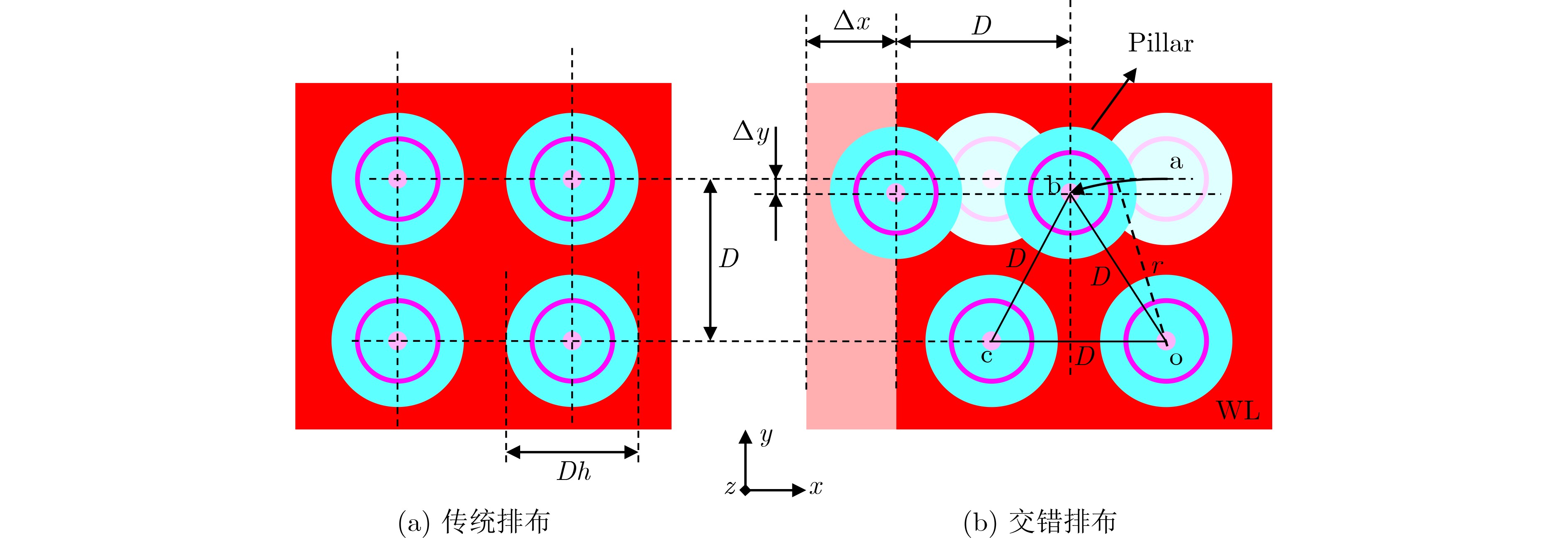
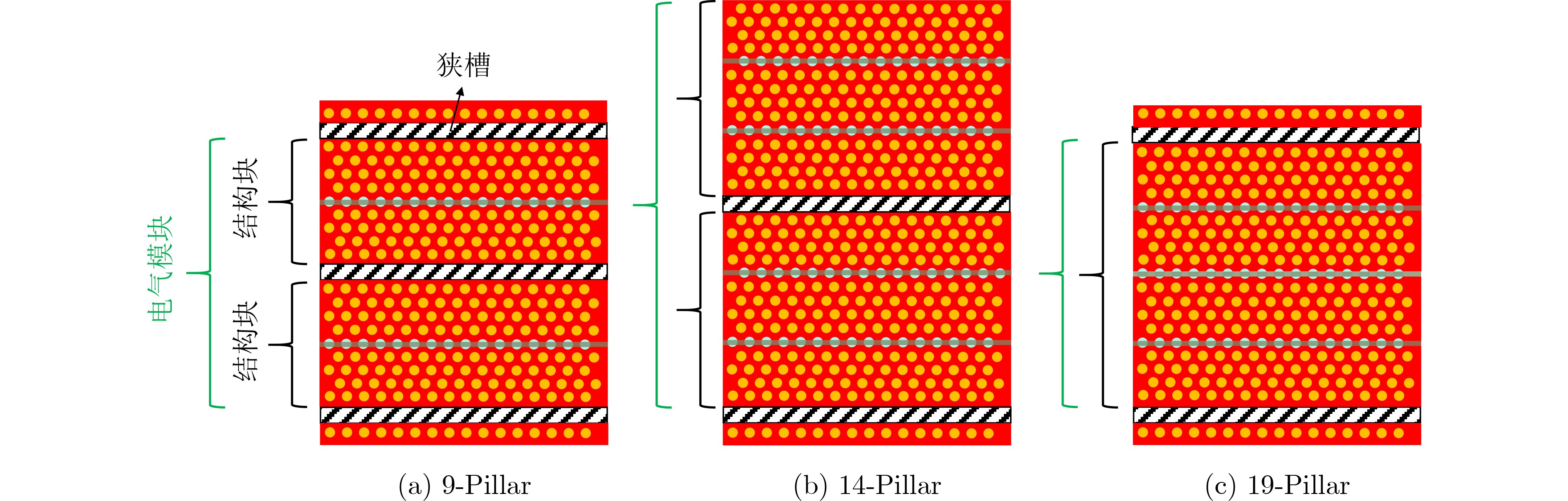
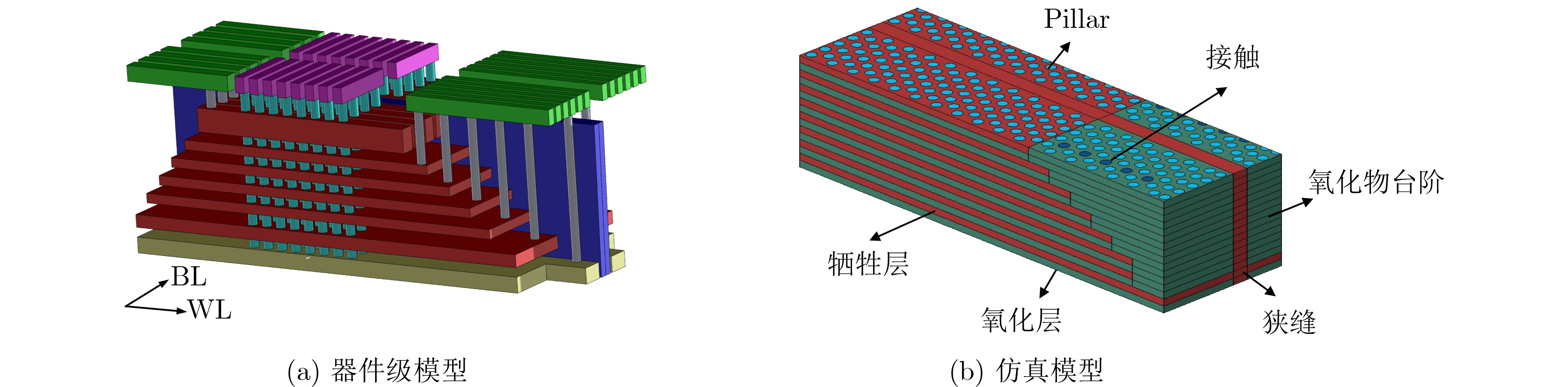
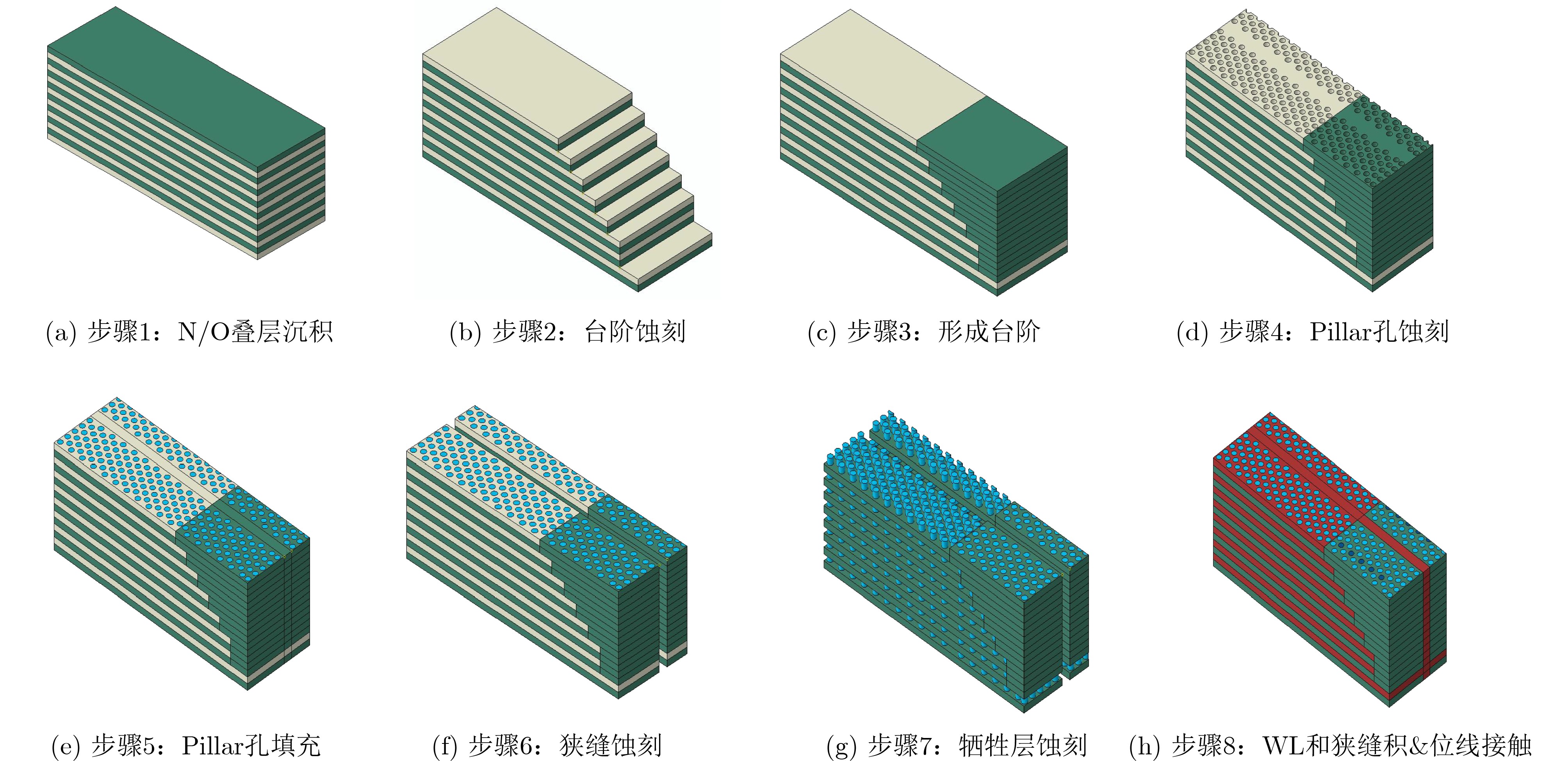
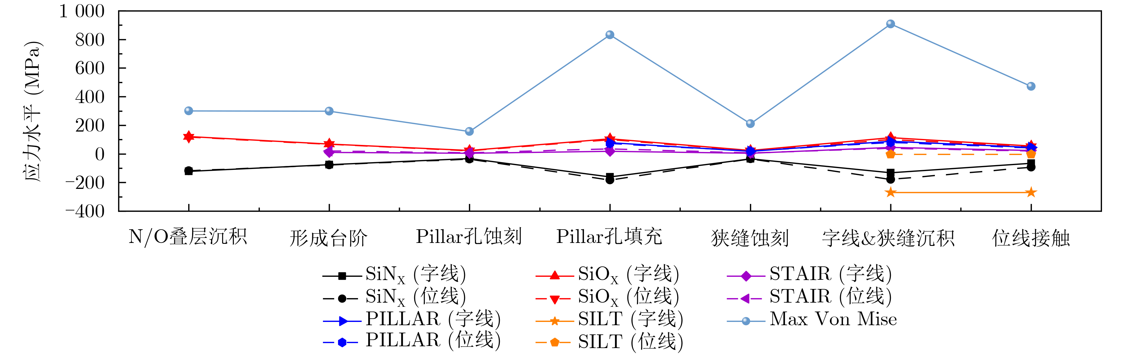
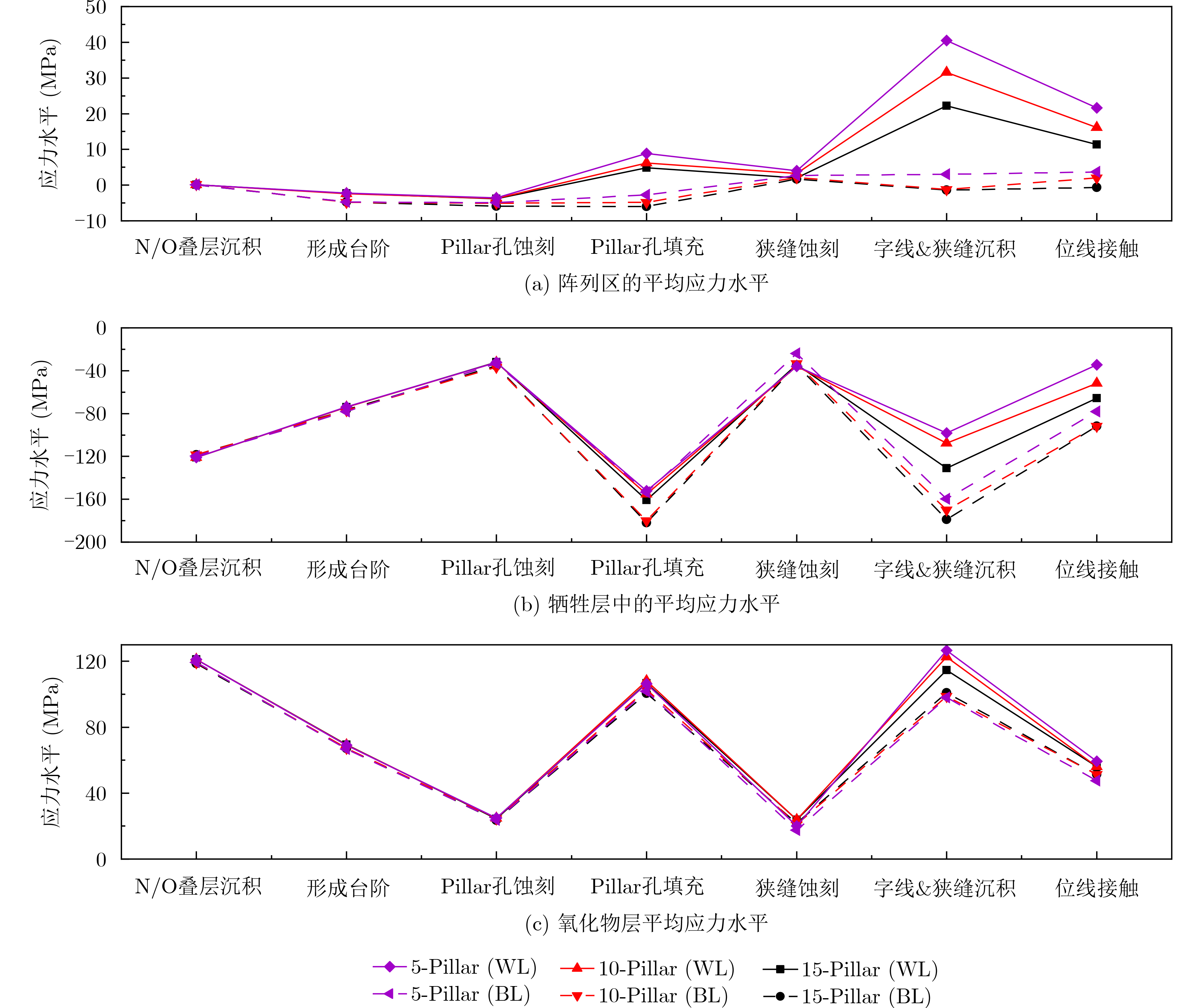
Objective To improve the performance of 3D NAND architecture, a series of horizontal and vertical miniaturization strategies have been proposed. While these designs increase storage density, they also introduce integration challenges. In particular, thermo-mechanical stress during fabrication has become a critical limitation on device yield and performance. This study establishes a high-precision process mechanics model of 3D NAND based on a local Representative Volume Element (RVE) finite element modeling framework, accounting for the multilayer stacked structure and various block architecture designs. By systematically investigating stress evolution during fabrication, the analysis identifies the root causes of stress non-uniformity and characterizes the dynamic distribution of mechanical stress under different miniaturization schemes. These findings have practical relevance for yield improvement and device reliability, addressing key challenges in advancing 3D NAND storage density. Methods This study constructs a high-precision, device-level finite element model of 3D NAND based on the theory of RVE. The simulation of thermal stress evolution throughout the manufacturing process uses the element birth/death technique in Abaqus. The baseline model features a representative 3D NAND structure comprising 8 Nitride/Oxide (N/O) bilayers, each 25 nm thick. Within a 40-nm-wide slit, 15 storage pillars, each with a diameter of 24 nm and spaced at 36 nm intervals, are arranged in a staggered configuration. To explore the effect of stacking layer number on stress evolution, modified models with 6 and 10 N/O layers are also developed. In addition, to examine the effect of different block architecture transitions, models incorporating 5 and 10 pillars per block are analyzed. The material properties used are consistent with those reported in previous studies, where both the calibration of material parameters and the modeling methodology are validated. Results and Discussions Process-dependent simulations were conducted to examine the evolution of stress distribution during key 3D NAND fabrication steps and to assess the effects of vertical stacking layers ( Fig. 7 ) and block architecture designs (Fig. 8 ). The results show that metal volume fraction, the number of pillars in the array region, and the presence of oxide stairs are primary factors influencing stress distribution. A higher metal volume fraction markedly increases internal stress due to thermal expansion mismatch. Asymmetric metal layouts in the Word Line (WL) and Bit Line (BL) directions intensify stress anisotropy between these axes. Pillars in the array region help alleviate stress concentration by generating tensile zones during nitride/metal thermal deformation, thereby reducing the overall compressive stress. In contrast, oxide stairs constrain deformation along the WL direction, inhibiting stress relaxation and resulting in localized compressive regions. These combined mechanisms indicate that increasing the number of WL layers tends to enhance stress asymmetry, whereas block architectures with a larger number of pillars reduce the degree of stress non-uniformity.Conclusions Using a process mechanics model based on the RVE approach, this study explored stress evolution in 3D NAND fabrication. The effects of two major scaling strategies—vertical layer stacking and horizontal block architecture conversion, were systematically analyzed with respect to stress magnitude and directional asymmetry. The results show that asymmetric stress distribution originates during the step etching stage and peaks following WL and slot filling. As the number of vertical stacking layers increases, structural compressive stress intensifies, particularly in the WL and BL directions. Increasing the number of layers from 6 to 10 results in an 8.54 MPa rise in WL compressive stress and a 5.66 MPa rise in BL stress, with the WL-BL stress difference increasing from 20.76 MPa to 24.64 MPa. Larger-area block architectures effectively mitigate stress asymmetry. Compared with the 5-pillar configuration, the 15-pillar architecture reduces WL-BL stress asymmetry by 22.4%. The composite structure of oxide and tungsten, combined with the constraint effects of pillars and stepped oxide on sacrificial layer deformation, plays a central role in modulating stress levels and directional distribution in 3D NAND structures. -
[1] MICHELONI R, ARITOME S, and CRIPPA L. Array architectures for 3-D NAND flash memories[J]. Proceedings of the IEEE, 2017, 105(9): 1634–1649. doi: 10.1109/JPROC.2017.2697000. [2] KURATA H, OTSUGA K, KOTABE A, et al. The impact of random telegraph signals on the scaling of multilevel flash memories[C]. The 2006 Symposium on VLSI Circuits, 2006. Digest of Technical Papers, Honolulu, USA, 2006: 112–113. doi: 10.1109/VLSIC.2006.1705335. [3] COMPAGNONI C M, SPINELLI A S, GUSMEROLI R, et al. Ultimate accuracy for the NAND flash program algorithm due to the electron injection statistics[J]. IEEE Transactions on Electron Devices, 2008, 55(10): 2695–2702. doi: 10.1109/TED.2008.2003230. [4] 卜伟海, 夏志良, 赵治国, 等. 后摩尔时代集成电路产业技术的发展趋势[J]. 前瞻科技, 2022, 1(3): 20–41. doi: 10.3981/j.issn.2097-0781.2022.03.002.BU Weihai, XIA Zhiliang, ZHAO Zhiguo, et al. Development of integrated circuit industrial technologies in the post-moore era[J]. Science and Technology Foresight, 2022, 1(3): 20–41. doi: 10.3981/j.issn.2097-0781.2022.03.002. [5] Samsung V-NAND technology[EB/OL]. http://www.samsung.com/us/business/oem-solutions/pdfs/VNAND_technology_WP.pdf. [6] JANG J, KIM H S, CHO W, et al. Vertical cell array using TCAT (Terabit Cell Array Transistor) technology for ultra high density NAND flash memory[C]. The 2009 Symposium on VLSI Technology, Kyoto, Japan , 2009: 192–193. [7] KANG Dongku, JEONG W, KIM C, et al. 256 Gb 3 b/cell V-NAND flash memory with 48 stacked WL layers[J]. IEEE Journal of Solid-State Circuits, 2017, 52(1): 210–217. doi: 10.1109/JSSC.2016.2604297. [8] KIM C, KIM D H, JEONG W, et al. A 512-Gb 3-b/cell 64-stacked WL 3-D-NAND flash memory[J]. IEEE Journal of Solid-State Circuits, 2018, 53(1): 124–133. doi: 10.1109/JSSC.2017.2731813. [9] PARK K T, NAM S, KIM D, et al. Three-dimensional 128 Gb MLC vertical NAND flash memory with 24-WL stacked layers and 50 MB/s high-speed programming[J]. IEEE Journal of Solid-State Circuits, 2015, 50(1): 204–213. doi: 10.1109/JSSC.2014.2352293. [10] PARK K T, BYEON D S, and KIM D H. A world’s first product of three-dimensional vertical NAND Flash memory and beyond[C]. The 14th Annual Non-Volatile Memory Technology Symposium (NVMTS), Jeju, Korea, 2014: 1–5. doi: 10.1109/NVMTS.2014.7060840. [11] MEYER R, FUKUZUMI Y, and DONG Yingda. 3D NAND Scaling in the next decade[C]. The 2022 International Electron Devices Meeting (IEDM), San Francisco, USA, 2022: 26.1. 1–26.1. 4. doi: 10.1109/IEDM45625.2022.10019570. [12] HEINECK L and LIU J. 3D NAND flash status and trends[C]. The 2022 IEEE International Memory Workshop (IMW), Dresden, Germany, 2022: 1–4. doi: 10.1109/IMW52921.2022.9779282. [13] 张源, 罗静茹, 张吉良. SDL PUF: 高可靠自适应偏差锁定PUF电路[J]. 电子与信息学报, 2024, 46(5): 2274–2280. doi: 10.11999/JEIT231313.ZHANG Yuan, LUO Jingru, and ZHANG Jiliang. SDL PUF: A high reliability self-adaption deviation locking PUF[J]. Journal of Electronics & Information Technology, 2024, 46(5): 2274–2280. doi: 10.11999/JEIT231313. [14] ZHANG Yuan, ZHONG Kuncai, and ZHANG Jiliang. DH-TRNG: A dynamic hybrid TRNG with ultra-high throughput and area-energy efficiency[C]. The 61st ACM/IEEE Design Automation Conference, San Francisco, USA, 2024: 1–6. doi: 10.1145/3649329.3656236. [15] LEE S H. Technology scaling challenges and opportunities of memory devices[C]. The 2016 IEEE International Electron Devices Meeting (IEDM), San Francisco, USA, 2016: 1.1. 1–1.1. 8. doi: 10.1109/IEDM.2016.7838026. [16] KRUV A, ARREGHINI A, VERRECK D, et al. Impact of mechanical stress on 3-D NAND flash current conduction[J]. IEEE Transactions on Electron Devices, 2020, 67(11): 4891–4896. doi: 10.1109/TED.2020.3024450. [17] ZHANG Kun, ZHOU Wenxi, LI Tuo, et al. Improvement of warpage and leakage for 3D NAND flash memory[J]. Materials Science in Semiconductor Processing, 2024, 176: 108294. doi: 10.1016/j.mssp.2024.108294. [18] SHI Wendian, ZHANG Haixia, ZHANG Guobing, et al. Modifying residual stress and stress gradient in LPCVD Si3N4 film with ion implantation[J]. Sensors and Actuators A: Physical, 2006, 130/131: 352–357. doi: 10.1016/j.sna.2005.10.008. [19] WU Kaiyi and POON A W. Stress-released Si3N4 fabrication process for dispersion-engineered integrated silicon photonics[J]. Optics Express, 2020, 28(12): 17708–17722. doi: 10.1364/OE.390171. [20] FAN Dongyu, XIA Zhiliang, YANG Tao, et al. An emerging local annealing method for simultaneous crystallization and activation in Xtacking 3-D NAND flash[J]. IEEE Transactions on Semiconductor Manufacturing, 2023, 36(1): 139–143. doi: 10.1109/TSM.2022.3229471. [21] KIM B, LEE S, HAH B, et al. 28.2 A high-performance 1Tb 3b/Cell 3D-NAND flash with a 194MB/s write throughput on over 300 layers i[C]. The 2023 IEEE International Solid-State Circuits Conference (ISSCC), San Francisco, USA, 2023: 27–29. doi: 10.1109/ISSCC42615.2023.10067666. [22] JANG E K, KIM I J, LEE C A, et al. Analysis of residual stresses induced in the confined 3D NAND flash memory structure for process optimization[J]. IEEE Journal of the Electron Devices Society, 2022, 10: 104–108. doi: 10.1109/JEDS.2022.3140774. [23] 李治昊, 夏志良, 许高博, 等. 3D NAND中基于SEG高度失效模型的DPPM预测算法[J]. 电子产品可靠性与环境试验, 2020, 38(6): 58–61. doi: 10.3969/j.issn.1672-5468.2020.06.015.LI Zhihao, XIA Zhiliang, XU Gaobo, et al. DPPM prediction algorithm based on SEG height failure model in 3D NAND[J]. Electronic Product Reliability and Environmental Testing, 2020, 38(6): 58–61. doi: 10.3969/j.issn.1672-5468.2020.06.015. [24] OKUDUR O O, GONZALEZ M, VAN DEN BOSCH G, et al. Multi-scale modeling approach to assess and mitigate wafer warpage in 3-D NAND fabrication[C]. The 2021 IEEE International Interconnect Technology Conference (IITC), Kyoto, Japan, 2021. doi: 10.1109/IITC51362.2021.9537435. [25] TIAN Zhiqiang, ZHANG Gang, HUANG Yuhua, et al. Process mechanics model and asymmetric residual stress analysis during 3-D NAND manufacturing[J]. IEEE Transactions on Electron Devices, 2025, 72(1): 193–198. doi: 10.1109/TED.2024.3496435. [26] CHU Weishen, RASHIDI S E E, ZHANG Yanli, et al. An analytical model for thin film pattern-dependent asymmetric wafer warpage prediction[C]. The 2022 IEEE International Memory Workshop (IMW), Dresden, Germany, 2022: 1–4. doi: 10.1109/IMW52921.2022.9779248. [27] OKUDUR O O, GONZALEZ M, VAN DEN BOSCH G, et al. Scaling-friendly approaches to minimize the magnitude and asymmetry of wafer warpage during 3-D NAND fabrication[J]. Microelectronics Reliability, 2023, 145: 114996. doi: 10.1016/j.microrel.2023.114996. -

 下载:
下载:


图(9) / 表(1)
计量
- 文章访问数: 1180
- HTML全文浏览量: 758
- PDF下载量: 117
- 被引次数: 0
