Two Highly Reliable Radiation Hardened By Design Static Random Access Memory Cells for Aerospace Applications
-
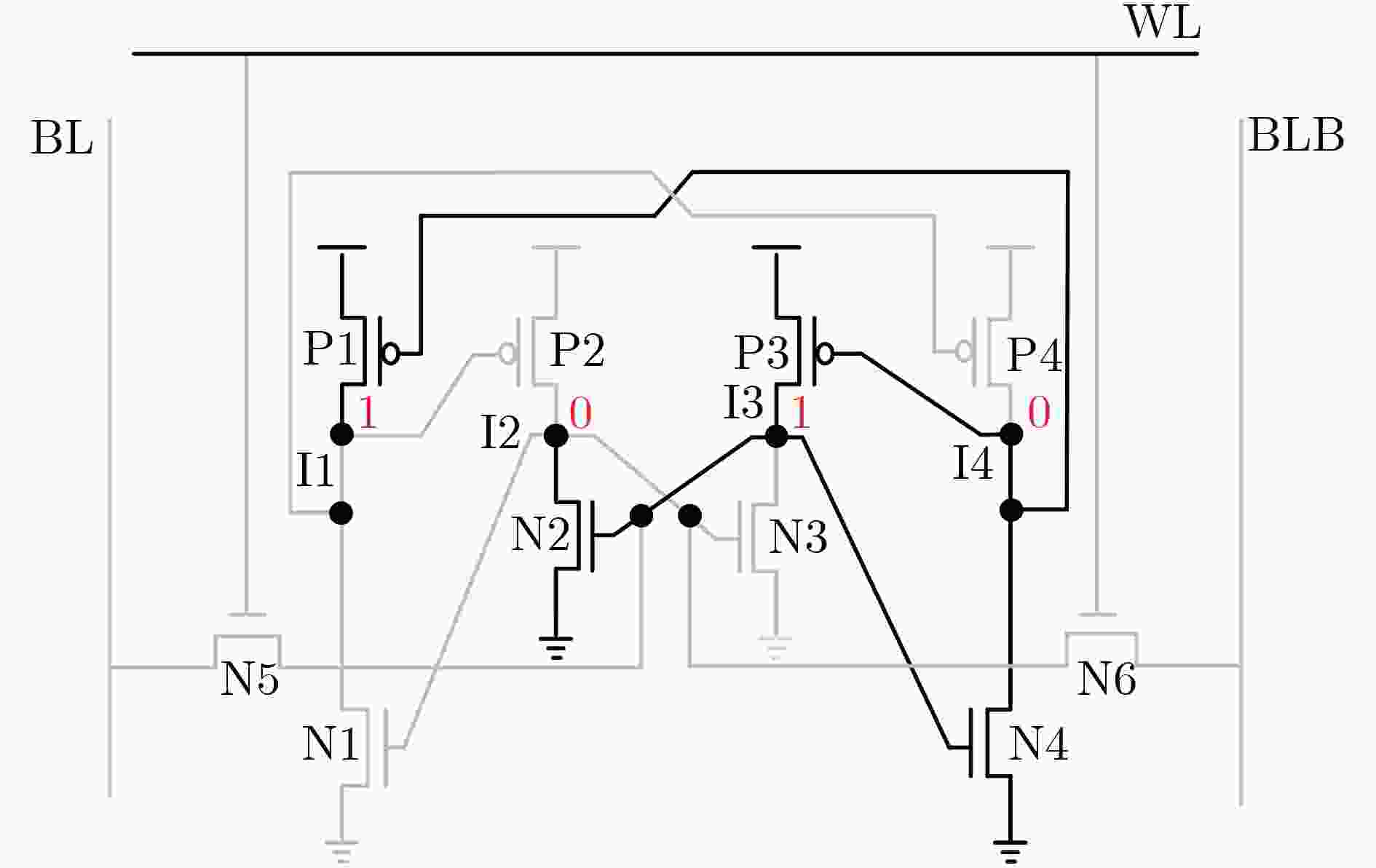
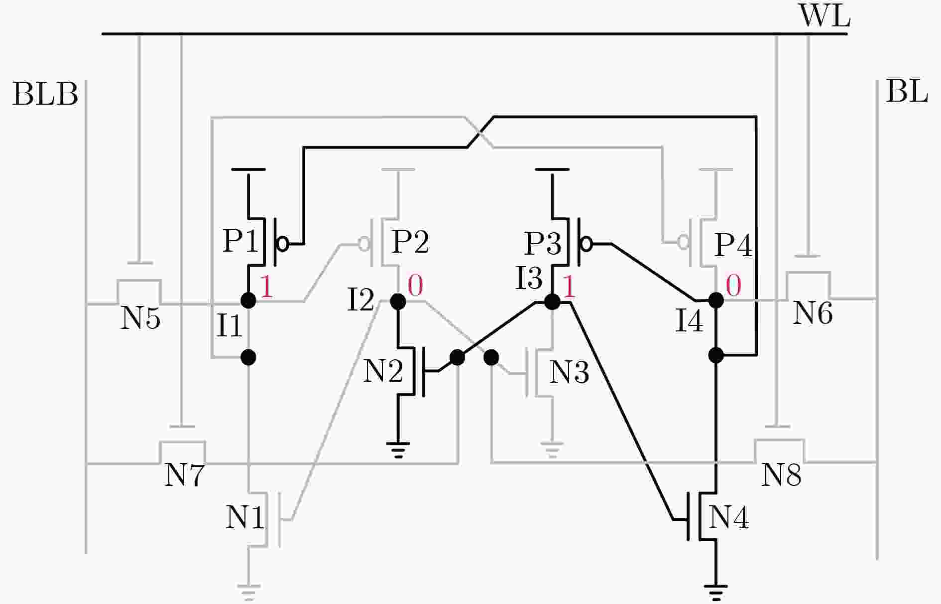
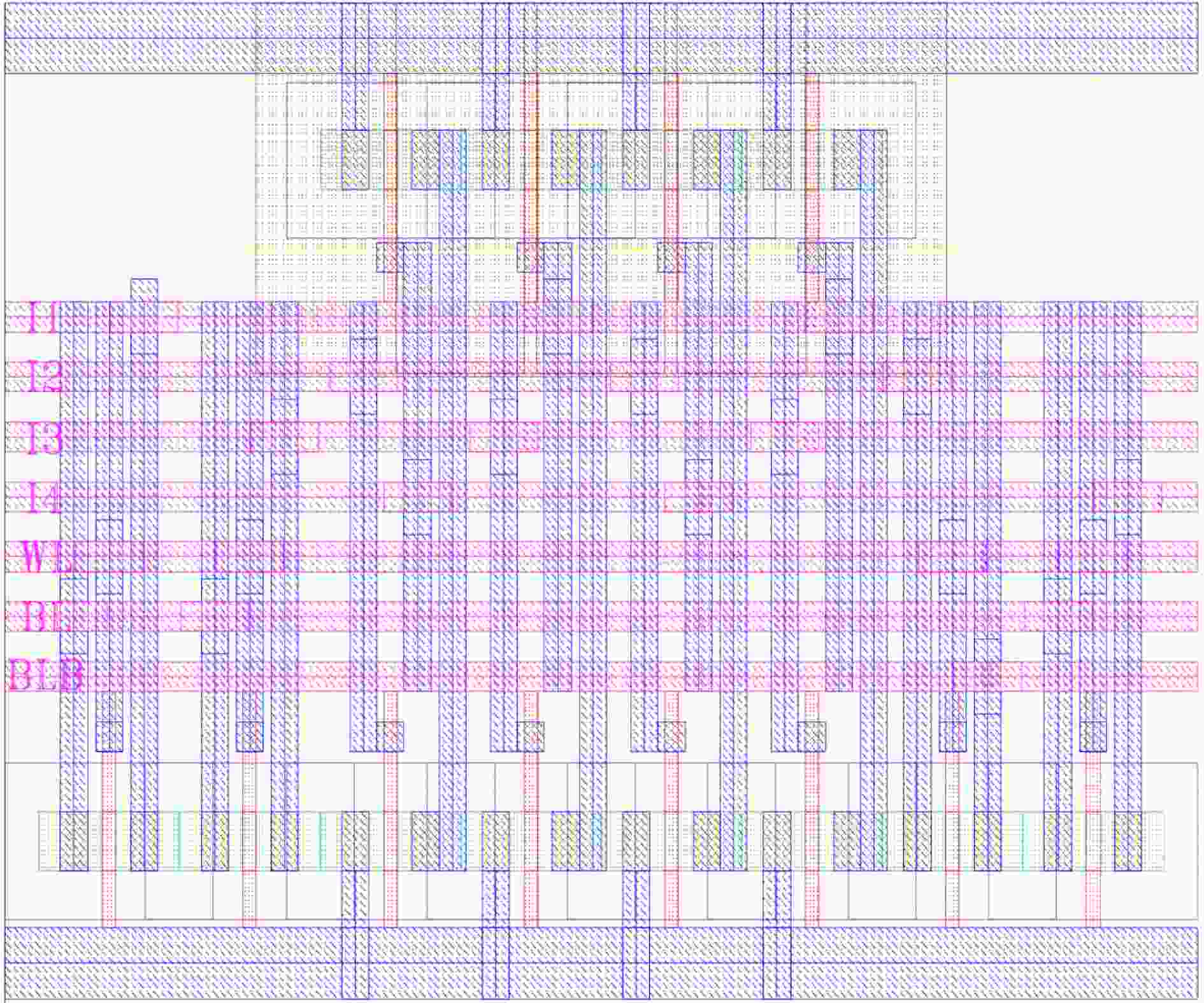
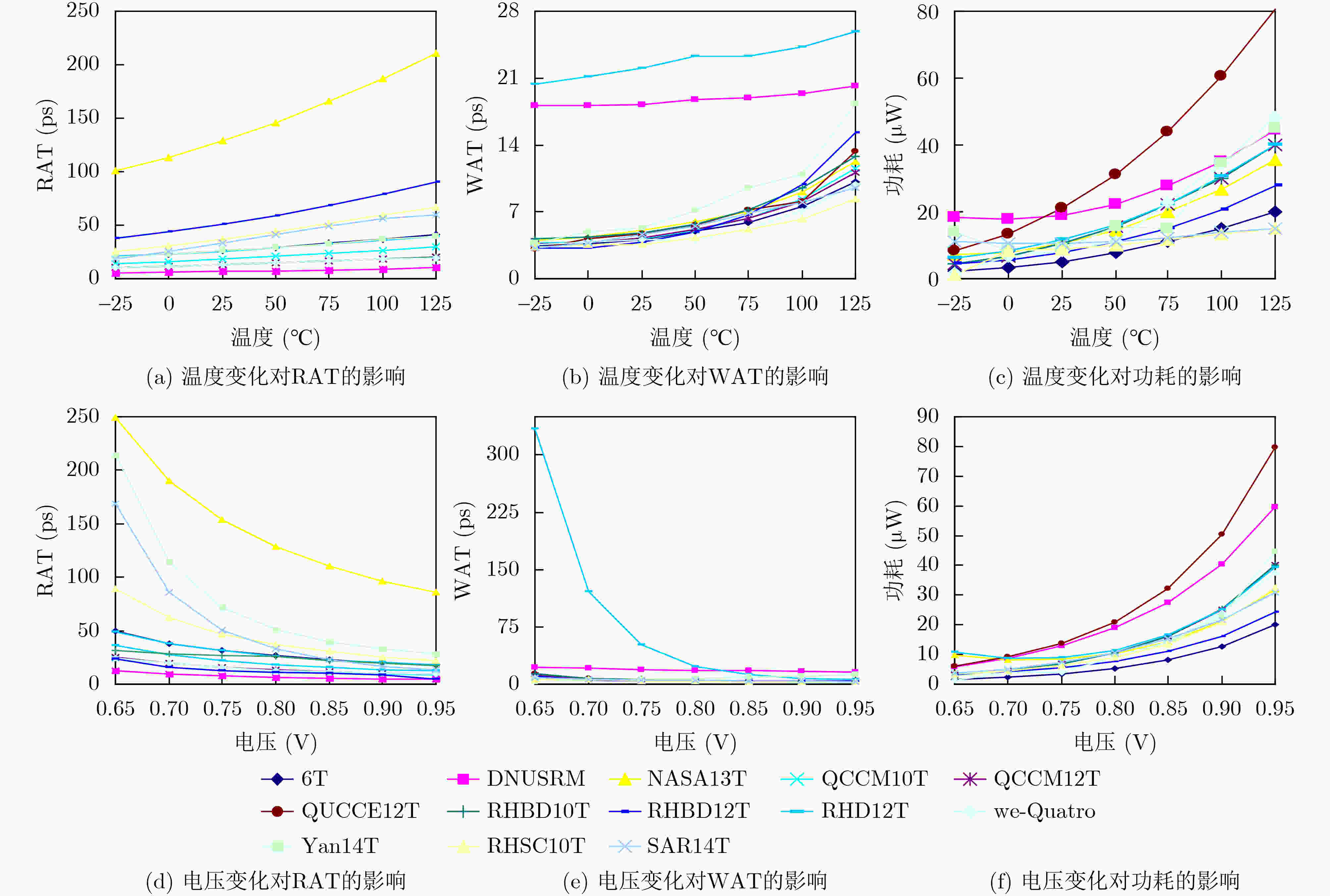
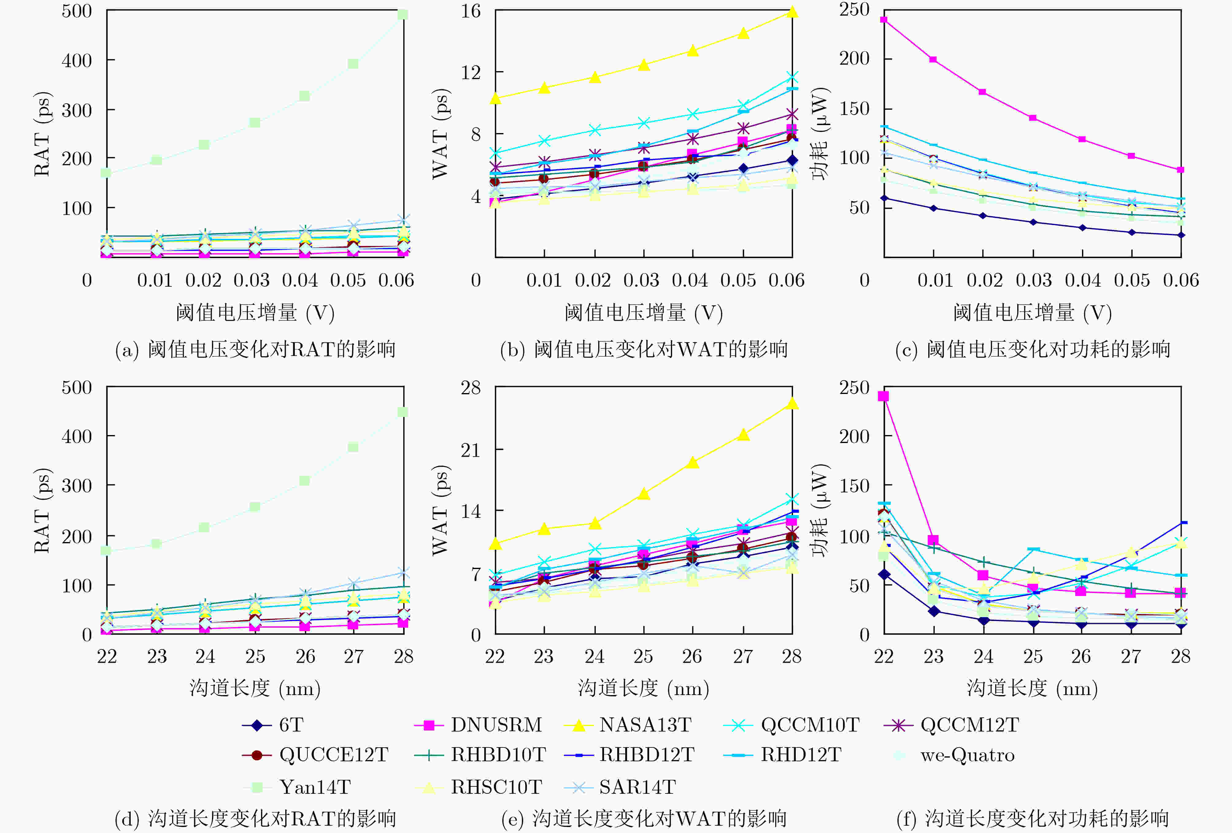
摘要: CMOS尺寸的大幅缩小引发电路可靠性问题。该文介绍了两种高可靠的基于设计的抗辐射加固(RHBD)10T和12T抗辐射加固技术(SRAM)单元,它们可以防护单节点翻转(SNU)和双节点翻转(DNU)。10T单元主要由两个交叉耦合的输入分离反相器组成,该单元可以通过其内部节点之间的反馈机制稳定地保持存储的值。由于仅使用少量晶体管,因此其在面积和功耗方面开销也较低。基于10T单元,提出了使用4个并行存取访问管的12T单元。与10T单元相比,12T单元的读/写访问时间更短,且具有相同的容错能力。仿真结果表明,所提单元可以从任意SNU和部分DNU中恢复。此外,与先进的加固SRAM单元相比,所提RHBD 12T单元平均可以节省16.8%的写访问时间、56.4%的读访问时间和10.2%的功耗,而平均牺牲了5.32%的硅面积。Abstract: Aggressive scaling of CMOS technologies can cause the reliability issues of circuits. Two highly reliable Radiation Hardened By Design (RHBD) 10T and 12T Static Random-Access Memory (SRAM) cells are presented in this paper, which can protect against Single Node Upsets (SNUs) and Double Node Upsets (DNUs). The 10T cell mainly consists of two cross-coupled input-split inverters and the cell can robustly keep stored values through a feedback mechanism among its internal nodes. It also has a low cost in terms of area and power consumption, since it uses only a few transistors. Based on the 10T cell, a 12T cell is proposed that uses four parallel access transistors. The 12T cell has a reduced read/write access time with the same soft error tolerance when compared to the 10T cell. Simulation results demonstrate that the proposed cells can recover from SNUs and a part of DNUs. Moreover, compared with the state-of-the-art hardened SRAM cells, the proposed RHBD 12T cell can save 16.8% write access time, 56.4% read access time, and 10.2% power dissipation at the cost of 5.32% silicon area on average.
-
表 1 未加固/加固 SRAM 单元之间的可靠性和开销比较结果
SRAM 6T NASA 13T RHD 12T QCCM 12T QUCCE 12T DNU SRM We-Quatro Yan 14T QCCM 10T RHSC 12T SAR 14T RHBD 10T RHBD 12T 文献 – [18] [19] [20] [21] [22] [23] [25] [20] [26] [27] 本文 本文 SNUR × × √ × × √ × × × √ √ √ √ #DHP 0 0 2 1 0 16 2 0 1 0 0 4 4 RAT (ps) 26.55 128.67 25.72 12.99 13.02 6.63 12.99 51.2 18.20 36.89 32.92 25.88 11.21 WAT (ps) 4.11 18.2 5.06 4.22 4.31 4.71 4.38 4.09 23.21 3.83 4.84 7.11 4.21 功耗(nW) 5.24 18.92 10.38 10.43 10.43 20.86 10.43 7.78 11.45 8.93 10.6 9.02 9.32 10–3×面积(nm2) 4.35 9.07 8.27 8.71 8.71 17.42 8.71 10.25 7.79 8.71 12.44 7.30 8.71 -
[1] YAN Aibin, FAN Zhengzheng, DING Liang, et al. Cost-effective and highly reliable circuit-components design for safety-critical applications[J]. IEEE Transactions on Aerospace and Electronic Systems, 2022, 58(1): 517–529. doi: 10.1109/TAES.2021.3103586. [2] VACCA E, AZIMI S, DE SIO C, et al. Soft error reliability prediction of SRAM-based FPGA designs[C]. 2022 22nd European Conference on Radiation and Its Effects on Components and Systems (RADECS), Venice, Italy, 2022: 1–4. doi: 10.1109/RADECS55911.2022.10412546. [3] WANG Shida, TANG Min, ZHANG Hongwei, et al. Evaluation of single-event upset in FinFET device[C]. 2023 5th International Conference on Radiation Effects of Electronic Devices (ICREED), Kunming, China, 2023: 1–7. doi: 10.1109/ICREED59404.2023.10390726. [4] LIANG Huaguo, XU Xiumin, HUANG Zhengfeng, et al. A methodology for characterization of SET propagation in SRAM-based FPGAs[J]. IEEE Transactions on Nuclear Science, 2016, 63(6): 2985–2992. doi: 10.1109/TNS.2016.2620165. [5] BLACK J D, DODD P E, and WARREN K M. Physics of multiple-node charge collection and impacts on single-event characterization and soft error rate prediction[J]. IEEE Transactions on Nuclear Science, 2013, 60(3): 1836–1851. doi: 10.1109/TNS.2013.2260357. [6] YAN Aibin, XU Zhelong, FENG Xiangfeng, et al. Novel quadruple-node-upset-tolerant latch designs with optimized overhead for reliable computing in harsh radiation environments[J]. IEEE Transactions on Emerging Topics in Computing, 2022, 10(1): 404–413. doi: 10.1109/TETC.2020.3025584. [7] HATEFINASAB S, MEDINA-GARCIA A, MORALES D P, et al. Rule-based design for low-cost double-node upset tolerant self-recoverable D-Latch[J]. IEEE Access, 2023, 11: 1732–1741. doi: 10.1109/ACCESS.2022.3233812. [8] ZEINZINGER M, LANGER J, EIBENSTEINER F, et al. Comparative analysis of SRAM PUF temperature susceptibility on embedded systems[C]. 2023 International Conference on Electrical, Computer and Energy Technologies (ICECET), Cape Town, South Africa, 2023: 1–8. doi: 10.1109/ICECET58911.2023.10389242. [9] SUGITANI S, NAKAJIMA R, YOSHIDA K, et al. Radiation hardened flip-flops with low area, delay and power overheads in a 65 nm bulk process[C]. 2023 IEEE International Reliability Physics Symposium (IRPS), Monterey, USA, 2023: 1–5. doi: 10.1109/IRPS48203.2023.10117957. [10] YAN Aibin, LING Yafei, CUI Jie, et al. Quadruple cross-coupled dual-interlocked-storage-cells-based multiple-node-upset-tolerant latch designs[J]. IEEE Transactions on Circuits and Systems I: Regular Papers, 2020, 67(3): 879–890. doi: 10.1109/TCSI.2019.2959007. [11] TIAN Yuanxin, ZHANG Yuejun, ZHANG Huihong, et al. An architecture of a single-event tolerant D flip-flop using full-custom design in 28nm process[C]. 2023 IEEE 15th International Conference on ASIC (ASICON), Nanjing, China, 2023: 1–4. doi: 10.1109/ASICON58565.2023.10396468. [12] LAI Xiaoling, GUO Yangming, ZHANG Jian, et al. A novel circuit and layout design of SEU tolerant SRAM in a 65nm CMOS process[C]. 2023 IEEE 18th Conference on Industrial Electronics and Applications (ICIEA), Ningbo, China, 2023: 522–526. doi: 10.1109/ICIEA58696.2023.10241793. [13] JUNG I S, KIM Y B, and LOMBARDI F. A novel sort error hardened 10T SRAM cells for low voltage operation[C]. IEEE 55th International Midwest Symposium on Circuits and Systems, Boise, USA, 2012: 714–717. doi: 10.1109/MWSCAS.2012.6292120. [14] LIN Sheng, KIM Y B, and LOMBARDI F. Analysis and design of nanoscale CMOS storage elements for single-event hardening with multiple-node upset[J]. IEEE Transactions on Device and Materials Reliability, 2012, 12(1): 68–77. doi: 10.1109/TDMR.2011.2167233. [15] RAJAEI R, ASGARI B, TABANDEH M, et al. Single event multiple upset-tolerant SRAM cell designs for nano-scale CMOS technology[J]. Turkish Journal of Electrical Engineering and Computer Sciences, 2017, 25(2): 1035–1047. doi: 10.3906/elk-1502-124. [16] GUO Jing, ZHU Lei, SUN Yu, et al. Design of area-efficient and highly reliable RHBD 10T memory cell for aerospace applications[J]. IEEE Transactions on Very Large Scale Integration (VLSI) Systems, 2018, 26(5): 991–994. doi: 10.1109/TVLSI.2017.2788439. [17] RAJAEI R, ASGARI B, TABANDEH M, et al. Design of robust SRAM cells against single-event multiple effects for nanometer technologies[J]. IEEE Transactions on Device and Materials Reliability, 2015, 15(3): 429–436. doi: 10.1109/TDMR.2015.2456832. [18] SHIYANOVSKII Y, RAJENDRAN A, and PAPACHRISTOU C. A low power memory cell design for SEU protection against radiation effects[C]. IEEE NASA/ESA Conference on Adaptive Hardware and Systems, Erlangen, Germany, 2012: 288–295. doi: 10.1109/AHS.2012.6268665. [19] QI Chunhua, XIAO Liyi, WANG Tianqi, et al. A highly reliable memory cell design combined with layout-level approach to tolerant single-event upsets[J]. IEEE Transactions on Device and Materials Reliability, 2016, 16(3): 388–395. doi: 10.1109/TDMR.2016.2593590. [20] YAN Aibin, ZHOU Jun, HU Yuanjie, et al. Novel quadruple cross-coupled memory cell designs with protection against single event upsets and double-node upsets[J]. IEEE Access, 2019, 7: 176188–176196. doi: 10.1109/access.2019.2958109. [21] JIANG Jianwei, XU Yiran, ZHU Wenyi, et al. Quadruple cross-coupled latch-based 10T and 12T SRAM bit-cell designs for highly reliable terrestrial applications[J]. IEEE Transactions on Circuits and Systems I: Regular Papers, 2019, 66(3): 967–977. doi: 10.1109/TCSI.2018.2872507. [22] YAN Aibin, WU Zhen, GUO Jing, et al. Novel double-node-upset-tolerant memory cell designs through radiation-hardening-by-design and layout[J]. IEEE Transactions on Reliability, 2019, 68(1): 354–363. doi: 10.1109/TR.2018.2876243. [23] DANG L D T, KIM J S, and CHANG I J. We-Quatro: Radiation-hardened SRAM cell with parametric process variation tolerance[J]. IEEE Transactions on Nuclear Science, 2017, 64(9): 2489–2496. doi: 10.1109/TNS.2017.2728180. [24] YAN Aibin, CHEN Yan, HU Yuanjie, et al. Novel speed-and-power-optimized SRAM cell designs with enhanced self-recoverability from single- and double-node upsets[J]. IEEE Transactions on Circuits and Systems I: Regular Papers, 2020, 67(12): 4684–4695. doi: 10.1109/TCSI.2020.3018328. [25] CHOUDHARY V and YADAV D S. Analysis of power, delay and SNM of 6T & 8T SRAM cells[C]. 2021 5th International Conference on Electronics, Communication and Aerospace Technology (ICECA), Coimbatore, India, 2021: 78–82. doi: 10.1109/ICECA52323.2021.9676022. [26] PRASAD G, MANDI B C, and ALI M. Design and analysis of 10T-boosted radiation hardened SRAM cell for aerospace applications[C]. 2019 IEEE International Symposium on Smart Electronic Systems (iSES) (Formerly iNiS), Rourkela, India, 2019: 304–307. doi: 10.1109/iSES47678.2019.00075. [27] PAL S, MOHAPATRA S, KI W H, et al. Soft-error-aware read-decoupled SRAM WITH MULTI-NODE RECOVERY FOR AEROSPACE APPLICATions[J]. IEEE Transactions on Circuits and Systems II: Express Briefs, 2021, 68(10): 3336–3340. doi: 10.1109/TCSII.2021.3073947. [28] 董攀, 范隆, 岳素格, 等. 一种高温单粒子效应测试系统的设计与实现[J]. 微电子学与计算机, 2011, 28(12): 17–20,24. doi: 10.19304/j.cnki.issn1000-7180.2011.12.005.DONG Pan, FAN Long, YUE Suge, et al. A high temperature single event effects test system design and implementation[J]. Microelectronics & Computer, 2011, 28(12): 17–20,24. doi: 10.19304/j.cnki.issn1000-7180.2011.12.005. [29] 刘冰燕, 蔡江铮, 黑勇. 应用于超低电压下的SRAM存储单元设计[J]. 微电子学与计算机, 2016, 33(9): 15–18,23. doi: 10.19304/j.cnki.issn1000-7180.2016.09.004.LIU Bingyan, CAI Jiangzheng, and HEI Yong. A SRAM bitcell design for ultra-low supply application[J]. Microelectronics & Computer, 2016, 33(9): 15–18,23. doi: 10.19304/j.cnki.issn1000-7180.2016.09.004. [30] PANDA S, KUMAR N M, and SARKAR C K. Power, delay and noise optimization of a SRAM cell using a different threshold voltages and high performance output noise reduction circuit[C]. 2009 4th International Conference on Computers and Devices for Communication (CODEC), Kolkata, India, 2009: 1–4. -


 下载:
下载:



 下载:
下载:
