Design of a Low-area and Low-delay Triple-Node-Upset Tolerant Latch
-
摘要: 随着纳米级CMOS集成电路的不断发展,锁存器极易受恶劣的辐射环境影响,由此引发的多节点翻转问题越来越严重。该文提出一种基于双联互锁存储单元(DICE)和2级C单元的3节点翻转(TNU)容忍锁存器,该锁存器包括5个传输门、2个DICE和3个C单元。该锁存器具有较小的晶体管数量,大大减小了电路的硬件开销,实现低成本。每个DICE单元可用来容忍并恢复单节点翻转,而C单元具有错误拦截特性,可屏蔽由DICE单元传来的错误值。当任意3个节点翻转后,借助DICE单元和C单元,该锁存器可容忍该错误。基于集成电路仿真程序(HSPICE)的仿真结果表明,与先进的TNU加固锁存器设计相比,该锁存器的延迟平均降低了64.65%,延迟功耗面积积平均降低了65.07%。Abstract: With the continuous development of nanoscale CMOS integrated circuits, latches are extremely susceptible to harsh radiation environment, and the multiple-node upset caused by radiation is becoming more and more serious. A Triple Node Upset (TNU) tolerant latch based on Dual-Interlocking CElls (DICEs) and dual-level C-elements is proposed. It includes five transmission gates, two DICEs, and three C-elements. The latch has a small number of transistors, which reduces greatly the hardware overhead of the latch to ensure low cost. Each DICE can be used to tolerate and recover from single-node upset, and the C-element has an error interception feature to mask erroneous values from DICEs. When any three nodes of the latch are upset, the latch can tolerate the TNU with the help of DICEs and C-elements. The simulation results using H-Simulation Program with Integrated Circuit Emphasis (HSPICE) show that, compared with the most advanced TNU tolerant latch designs, the delay is reduced by 64.65%, and the delay power area product is reduced by 65.07% for the proposed latch on average.
-
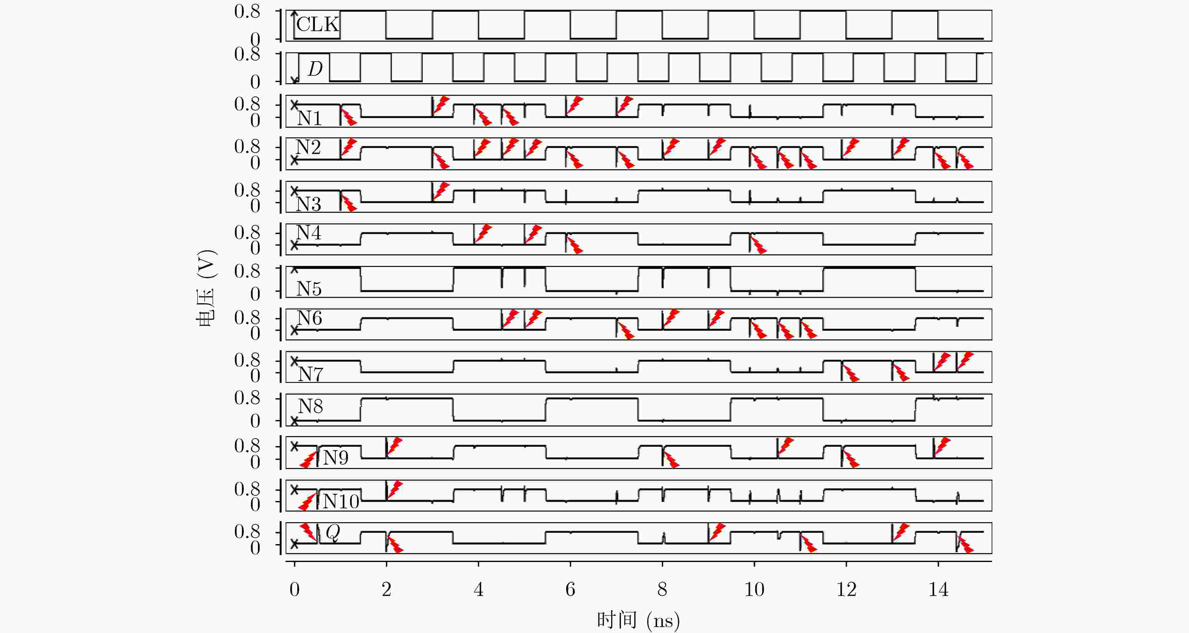
表 1 锁存器可靠性对比结果
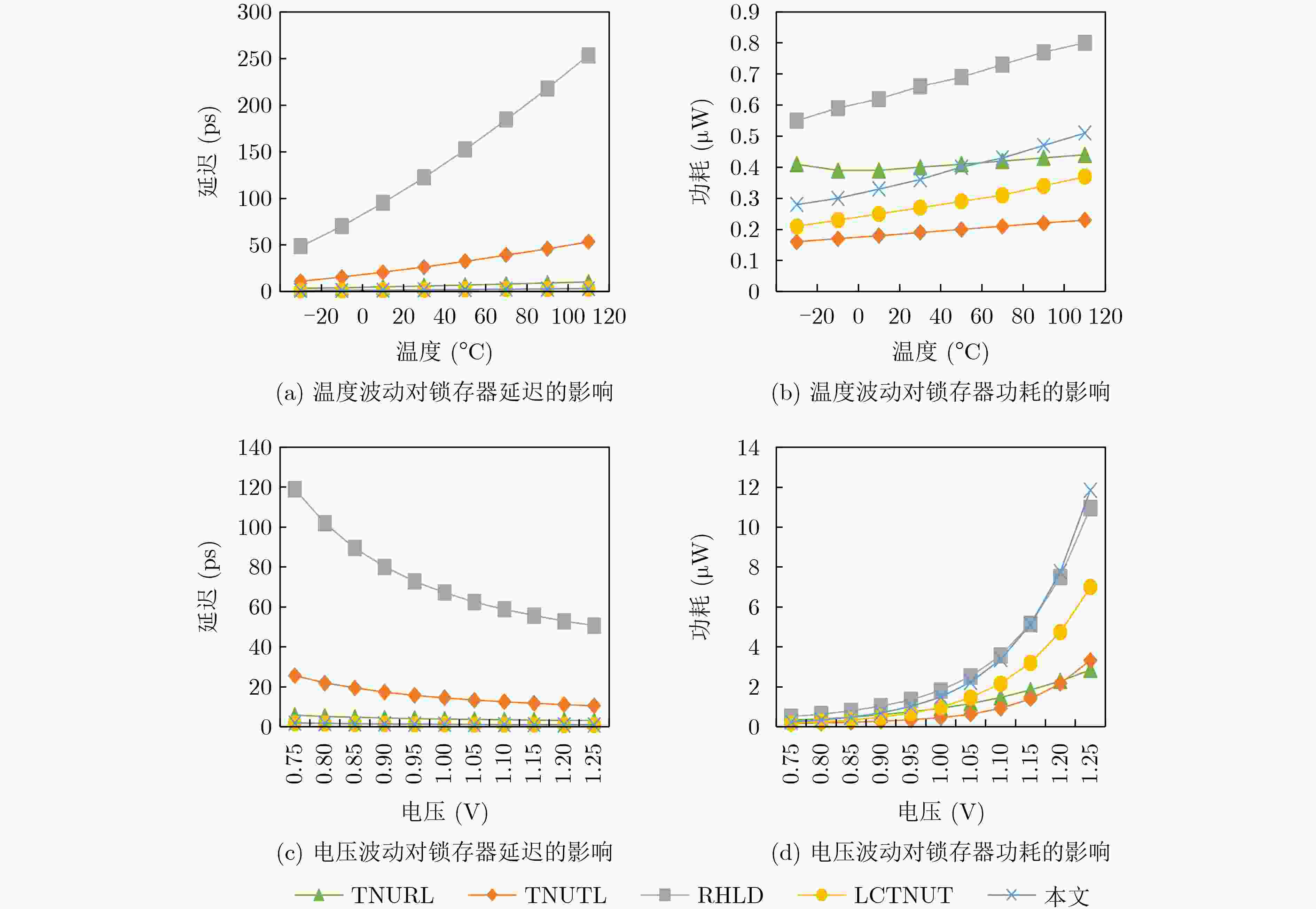
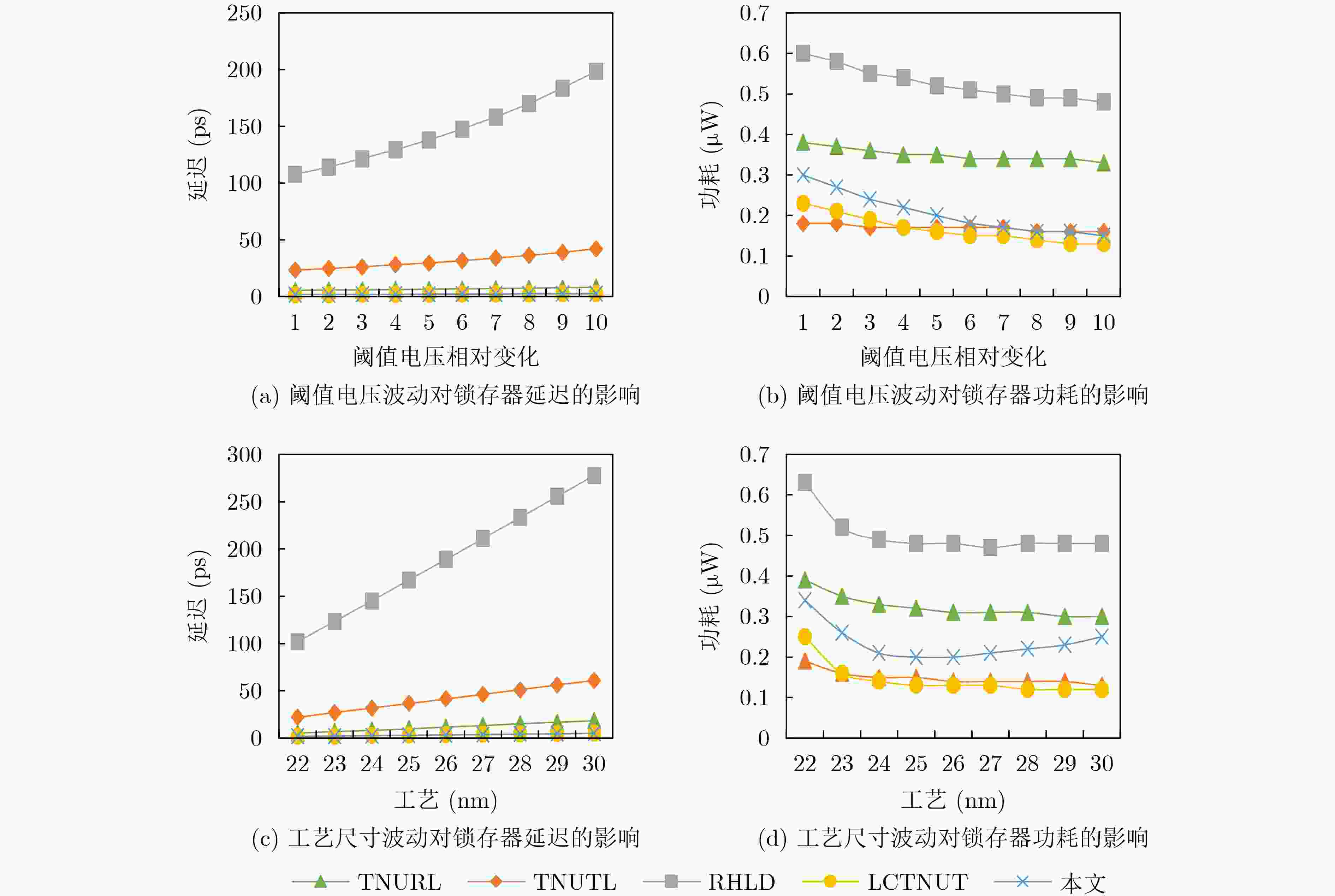
表 2 锁存器性能参数对比结果
锁存器 D-Q 延迟(ps) 功耗(μW) 面积(×10–4 nm2) DPAP (×10–6) D锁存器 11.80 0.11 0.66 0.009 FERST 41.39 0.20 1.85 0.153 ISEHL 2.90 0.12 1.58 0.005 TMR 46.42 0.70 3.70 1.202 HRUT 58.23 0.22 1.98 0.254 DNUR 3.01 0.44 4.36 0.058 TNUTL 21.95 0.19 2.38 0.099 RHLD 101.86 0.63 5.41 3.472 LCTNUT 1.67 0.25 3.17 0.013 TNURL 5.20 0.39 8.45 0.171 本文 1.67 0.34 2.64 0.015 表 3 抗TNU锁存器的相对开销比较(%)
锁存器 D–Q 延迟 功耗 面积(×10–4) DPAP TNUTL –92.39 78.95 10.92 –84.85 RHLD –98.36 –46.03 –51.20 –99.57 LCTNUT 0.00 36.00 –16.72 15.38 TNURL –67.88 –12.82 –68.76 –91.23 平均 –64.65 14.03 –31.44 –65.07 表 4 抗TNU锁存器的静态功耗和动态功耗(μW)
锁存器 静态功耗 动态功耗 平均功耗 TNUTL 0.050 0.140 0.19 RHLD 0.062 0.568 0.63 LCTNUT 0.075 0.175 0.25 TNURL 0.055 0.335 0.39 本文 0.058 0.282 0.34 -
[1] YAN Aibin, FENG Xiangfeng, HU Yuanjie, et al. Design of a triple-node-upset self-recoverable latch for aerospace applications in harsh radiation environments[J]. IEEE Transactions on Aerospace and Electronic Systems, 2020, 56(2): 1163–1171. doi: 10.1109/TAES.2019.2925448 [2] 黄正峰, 郭阳, 李雪筠, 等. 单粒子四点翻转自恢复加固锁存器设计[J]. 计算机辅助设计与图形学学报, 2021, 33(4): 632–639. doi: 10.3724/SP.J.1089.2021.18573HUANG Zhengfeng, GUO Yang, LI Xuejun, et al. Single-event quadruple-upset self-recoverable latch design[J]. Journal of Computer-Aided Design &Computer Graphics, 2021, 33(4): 632–639. doi: 10.3724/SP.J.1089.2021.18573 [3] 黄正峰, 曹迪, 崔建国, 等. 32 nm CMOS工艺的单粒子多点翻转加固锁存器设计[J]. 计算机辅助设计与图形学学报, 2021, 33(3): 346–355. doi: 10.3724/SP.J.1089.2021.18385HUANG Zhengfeng, CAO Di, CUI Jianguo, et al. Design of multiple node upset tolerant latch in 32 nm CMOS technology[J]. Journal of Computer-Aided Design &Computer Graphics, 2021, 33(3): 346–355. doi: 10.3724/SP.J.1089.2021.18385 [4] 郭靖, 李强, 宿晓慧, 等. 新型RHBD抗多节点翻转锁存器设计[J]. 计算机辅助设计与图形学学报, 2021, 33(6): 963–973. doi: 10.3724/SP.J.1089.2021.18615GUO Jing, LI Qiang, SU Xiaohui, et al. Novel radiation hardening by design latch for tolerating multiple-node upset[J]. Journal of Computer-Aided Design &Computer Graphics, 2021, 33(6): 963–973. doi: 10.3724/SP.J.1089.2021.18615 [5] 黄正峰, 潘尚杰, 曹剑飞, 等. 32nm CMOS 工艺三点翻转自恢复锁存器设计[J]. 电子学报, 2021, 49(2): 394–400. doi: 10.12263/DZXB.20200530HUANG Zhengfeng, PAN Shangjie, CAO Jianfei, et al. Design of triple-node-upset self-recovery latch in 32 nm CMOS technology[J]. Acta Electronica Sinica, 2021, 49(2): 394–400. doi: 10.12263/DZXB.20200530 [6] YAN Aibin, HU Yuanjie, CUI Jie, et al. Information assurance through redundant design: A novel TNU error-resilient latch for harsh radiation environment[J]. IEEE Transactions on Computers, 2020, 69(6): 789–799. doi: 10.1109/TC.2020.2966200 [7] FAZELI M, MIREMADI S G, EJLALI A, et al. Low energy single event upset/single event transient-tolerant latch for deep submicron technologies[J]. IET Computers & Digital Techniques, 2009, 3(3): 289–303. doi: 10.1049/iet-cdt.2008.0099 [8] EFTAXIOPOULOS N, AXELOS N, ZERVAKIS G, et al. Delta DICE: A double node upset resilient latch[C]. The 58th International Midwest Symposium on Circuits and Systems, Fort Collins, USA, 2015: 1–4. [9] KATSAROU K and TSIATOUHAS Y. Double node charge sharing SEU tolerant latch design[C]. The IEEE 20th International On-Line Testing Symposium, Platja d'Aro, Spain, 2014: 122–127. [10] XU Hui and ZENG Yun. Circuit and layout combination technique to enhance multiple nodes upset tolerance in latches[J]. IEICE Electronics Express, 2015, 12(9): 20150286. doi: 10.1587/elex.12.20150286 [11] WATKINS A and TRAGOUDAS S. Radiation hardened latch designs for double and triple node upsets[J]. IEEE Transactions on Emerging Topics in Computing, 2020, 8(3): 616–626. doi: 10.1109/TETC.2017.2776285 [12] CALIN T, NICOLAIDIS M, and VELAZCO R. Upset hardened memory design for submicron CMOS technology[J]. IEEE Transactions on Nuclear Science, 1996, 43(6): 2874–2878. doi: 10.1109/23.556880 [13] YAN Aibin, LAI Chaoping, ZHANG Yinlei, et al. Novel low cost, double-and-triple-node-upset-tolerant latch designs for nano-scale CMOS[J]. IEEE Transactions on Emerging Topics in Computing, 2021, 9(1): 520–533. doi: 10.1109/TETC.2018.2871861 [14] KUMAR C I and ANAND B. A highly reliable and energy-efficient triple-node-upset-tolerant latch design[J]. IEEE Transactions on Nuclear Science, 2019, 66(10): 2196–2206. doi: 10.1109/TNS.2019.2939380 [15] YAN Aibin, XU Zhelong, FENG Xiangfeng, et al. Novel quadruple-node-upset-tolerant latch designs with optimized overhead for reliable computing in harsh radiation environments[J]. IEEE Transactions on Emerging Topics in Computing, 2022, 10(1): 404–413. doi: 10.1109/TETC.2020.3025584 [16] YAN Aibin, LI Zhixing, CUI Jie, et al. Designs of two quadruple-node-upset self-recoverable latches for highly robust computing in harsh radiation environments[J]. IEEE Transactions on Aerospace and Electronic Systems, 2023, 59(3): 2885–2897. doi: 10.1109/TAES.2022.3219372 [17] 黄正峰, 姚慧杰, 李先东, 等. 一种高性能低功耗的双节点翻转加固锁存器[J]. 合肥工业大学学报:自然科学版, 2019, 42(12): 1649–1654. doi: 10.3969/j.issn.1003-5060.2019.12.012HUANG Zhengfeng, YAO Huijie, LI Xiandong, et al. HLDRL latch: A high performance, low cost, double node upset resilient latch[J]. Journal of Hefei University of Technology:Natural Science, 2019, 42(12): 1649–1654. doi: 10.3969/j.issn.1003-5060.2019.12.012 [18] YAN Aibin, HUANG Zhengfeng, YI Maoxiang, et al. Double-node-upset-resilient latch design for nanoscale CMOS technology[J]. IEEE Transactions on Very Large Scale Integration (VLSI) Systems, 2017, 25(6): 1978–1982. doi: 10.1109/TVLSI.2017.2655079 [19] LIANG Huaguo, WANG Zhi, HUANG Zhengfeng, et al. Design of a radiation hardened latch for low-power circuits[C]. The IEEE 23rd Asian Test Symposium, Hangzhou, China, 2014: 19–24. [20] SHE Xiaoxuan and MCELVAIN K S. Time multiplexed triple modular redundancy for single event upset mitigation[J]. IEEE Transactions on Nuclear Science, 2009, 56(4): 2443–2448. doi: 10.1109/TNS.2009.2021656 [21] RAJAEI R, TABANDEH M, and FAZELI M. Single event multiple upset (SEMU) tolerant latch designs in presence of process and temperature variations[J]. Journal of Circuits, Systems and Computers, 2015, 24(1): 1550007. doi: 10.1142/S0218126615500073 [22] LIU Xin. Multiple node upset-tolerant latch design[J]. IEEE Transactions on Device and Materials Reliability, 2019, 19(2): 387–392. doi: 10.1109/TDMR.2019.2912811 -


 下载:
下载:




 下载:
下载:
