High-speed Fully Differential Two-step ADC Design Method for CMOS Image Sensor
-
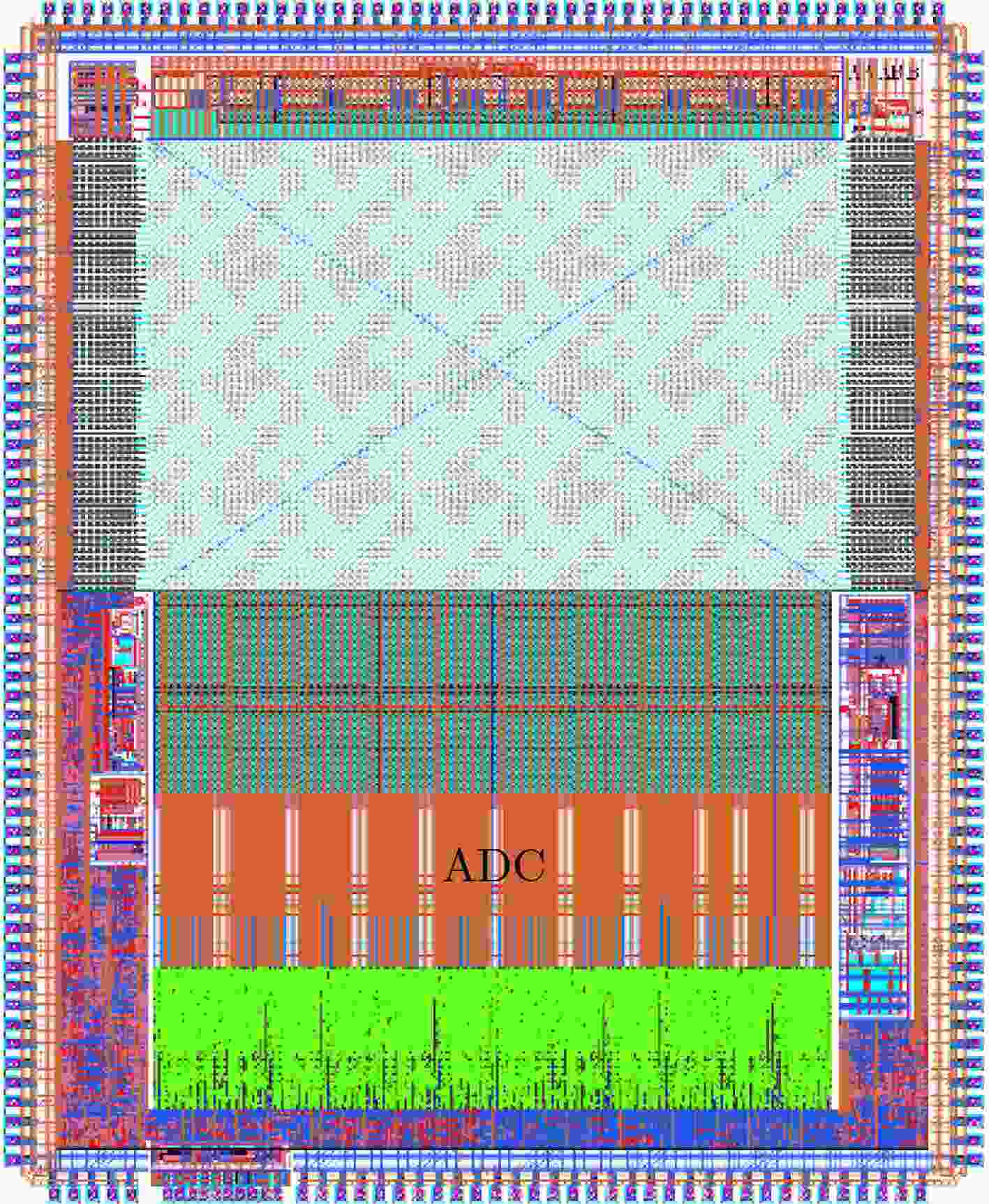
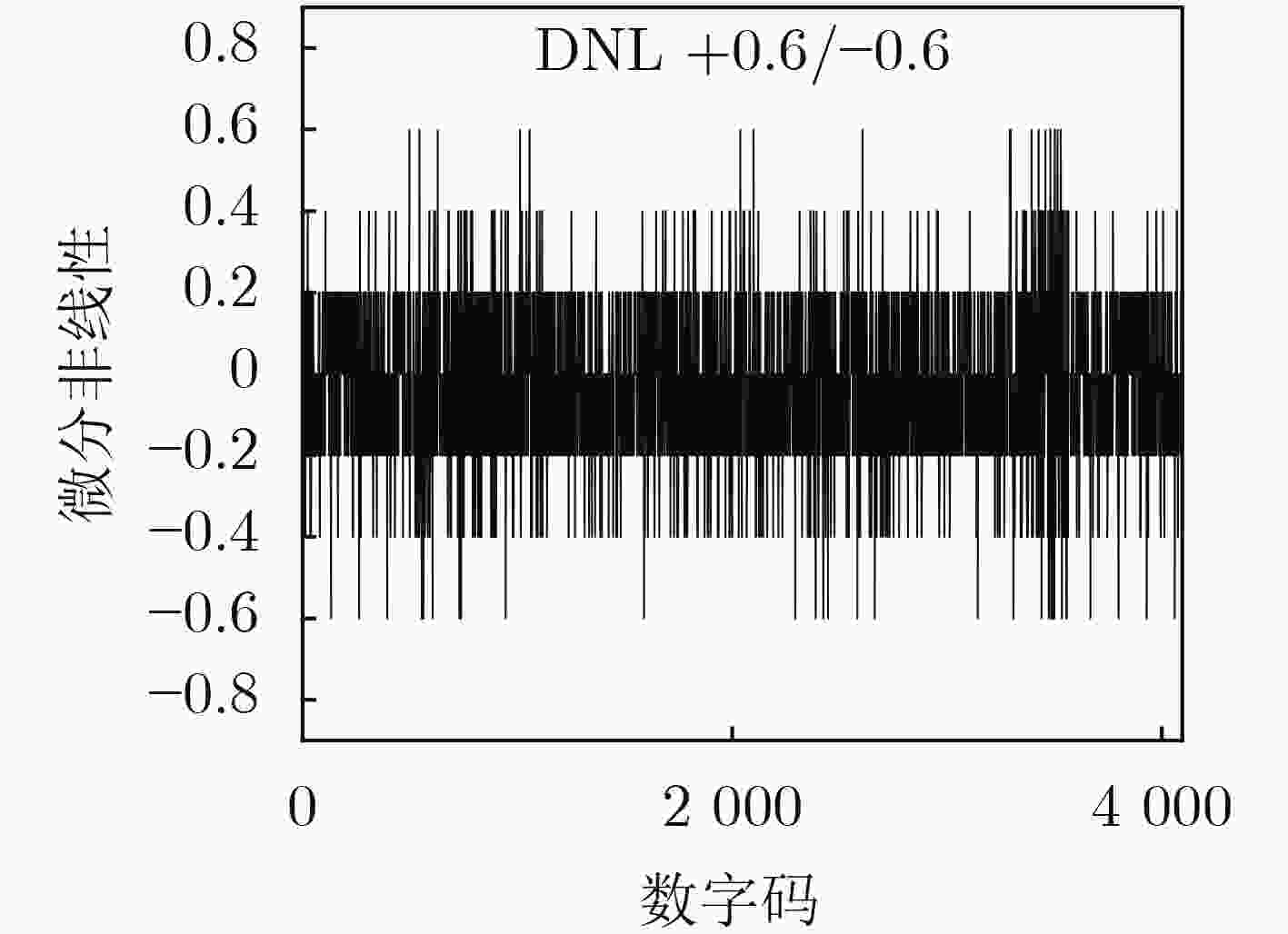
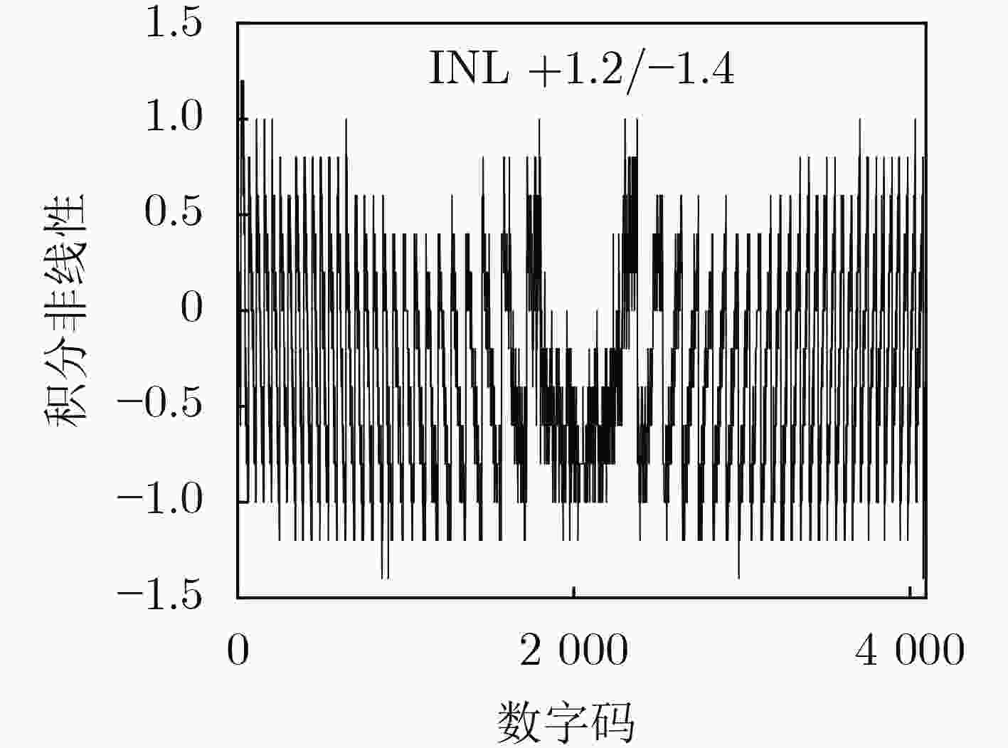
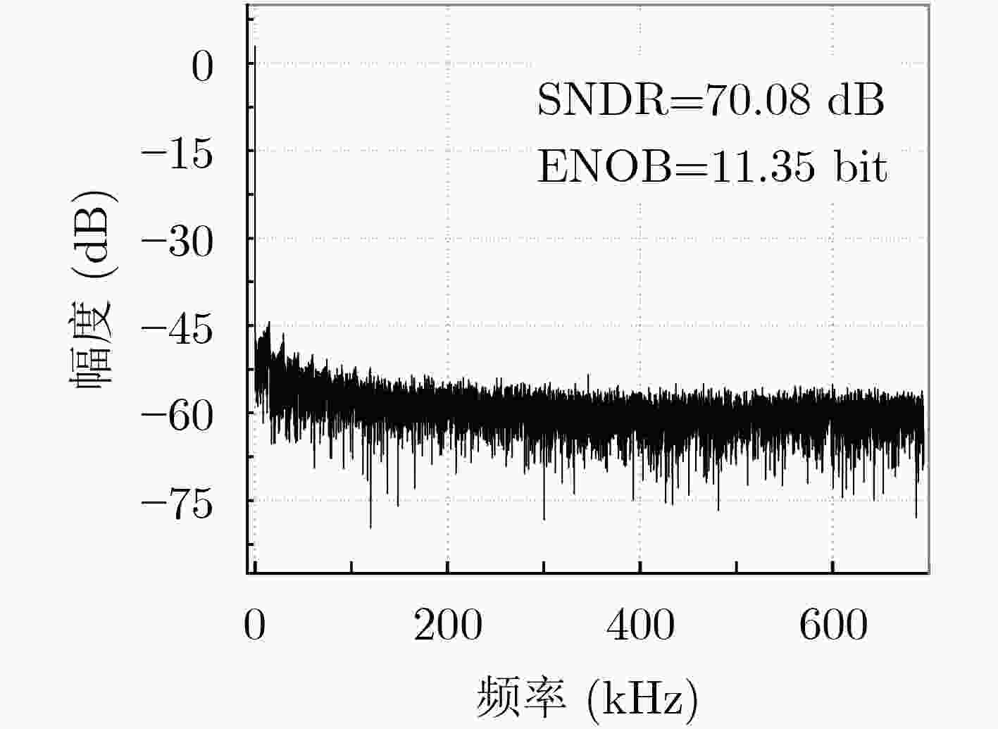
摘要: 由于传统的单斜式模数转换器(SS ADC)以及改进的各种架构串行两步式SS ADC普遍存在速度瓶颈问题,均无法满足工业界高帧率CMOS图像传感器的发展需求,该文提出一种应用于高帧率CMOS图像传感器的高速全差分两步式ADC设计方法。该ADC设计方法基于差动斜坡与时间数字转换(TDC)技术,将差动量化嵌套在两步式的量化中,形成了区别于串行量化的并行量化模式,不仅提升了数据量化的速率,而且保证了系统的一致性和鲁棒性;针对传统TDC技术与单斜式ADC的匹配性问题,提出了一种基于电平编码的TDC技术,在ADC量化的最后一个时钟周期内,在不提升系统时钟的情况下,完成时间数字转换,实现了更高精度的量化。该文基于55 nm 1P4M CMOS实验平台完成了所提方法的电路设计、版图设计和测试验证。在模拟电压3.3 V、数字电压1.2 V、时钟频率100 MHz、动态输入范围1.6 V的设计环境下,该文ADC设计精度为12 bit,转换时间仅有480 ns,列级功耗低至62 μW,DNL以最低有效位(LSB)计为+0.6/–0.6,INL以最低有效位(LSB)计为+1.2/–1.4,信噪失真比(SNDR)达到70.08 dB,与现有的先进单斜式ADC相比,ADC转换速度提高了52%以上,可以有效压缩行处理时间,为高帧率大面阵CMOS图像传感器的实现提供了有效的解决方案。Abstract: Due to the common speed bottleneck problem of traditional Single-Slope Analog-to-Digital Converter (SS ADC) and serial two-step ADC, the application requirements of high frame rate CMOS Image Sensor (CIS) in the industry have not been met. In this paper, a high-speed fully differential two-step ADC design method for CIS is proposed. The ADC design method is based on differential ramp and Time-to-Digital Conversion (TDC) technology. A parallel conversion mode is formed, which is different from serial conversion, and the robustness of the system is ensured due to the existence of differential ramps. Focusing on the inconsistency between traditional TDC technology and single-slope ADC, a TDC technology based on level coding is proposed, which completes time-to-digital conversion in the last clock cycle of A/D conversion, and realizes a two-step conversion process at another level. Based on the 55 nm 1P4M CMOS experimental platform, this paper completes the circuit design, layout design and test verification of the proposed design method. Under the design environment of analog voltage 3.3 V, digital voltage 1.2 V, clock frequency 100MHz, and dynamic input range 1.6 V, this design is a 12 bit ADC, the conversion time is 480 ns, the column-level power consumption is 62 μW, the DNL (Differential Non-Linearity is measured in the Least Significant Bit) is +0.6/–0.6, the INL (Integral Non-Linearity is measured in the Least Significant Bit) is +1.2/–1.4, and the Signal-to-Noise Distortion Ratio (SNDR) reaches 70.08 dB. Compared with the existing advanced single-slope ADC, the ADC conversion speed is increased by more than 52%, which is a large area array with high frame rate. It provides an effective solution for the implementation of high frame frequency CIS.
-
Key words:
- CMOS Image Sensor(CIS) /
- Differential ramp /
- Time-to-Digital Conversion(TDC) /
- Level encoding /
- Two-step
-
表 1 本文设计方法与文献的对比结果
文献[22] 文献[23] 文献[24] 文献[1] 本文 工艺(nm) 130 – 55 130 55 结构 两步式 两步式 全并行两步式 单斜式+TDC 全差分两步式+TDC ADC 精度(bit) 12 12 12 12 12 量化范围(V) 1.2 – 1.472 – 1.6 转换时间 10 μs 6.38 μs 1.28 μs 1 μs 480 ns DNL 0.76/–0.8 +1.34/–0.49 +0.8/–0.8 +1.1/–0.4 +0.6/–0.6 INL 1.06/–0.84 +2.44/–2.47 +2.1/–3.5 +5.8/–8.2 +1.2/–1.4 有效位数(bit) 11.25 – 11.33 – 11.35 功耗(μW) 72 112.5 47 177 62 品质因数*( pJ/conv.-step) 0.296 0.175 0.023 0.043 0.008 *=功耗/(采样率×2有效位数) -
[1] LEVSKI D, WÄNY M, and CHOUBEY B. A 1-μs ramp time 12-bit column-parallel flash TDC-interpolated single-slope ADC with digital delay-element calibration[J]. IEEE Transactions on Circuits and Systems I:Regular Papers, 2019, 66(1): 54–67. doi: 10.1109/TCSI.2018.2846592 [2] KAUR A, MISHRA D, and SARKAR M. A 12-bit, 2.5-bit/phase column-parallel cyclic ADC[J]. IEEE Transactions on Very Large Scale Integration (VLSI) Systems, 2019, 27(1): 248–252. doi: 10.1109/TVLSI.2018.2871341 [3] OKADA C, UEMURA K, HUNG L, et al. 7.6 a high-speed back-illuminated stacked CMOS image sensor with column-parallel kT/C-cancelling S&H and delta-sigma ADC[C] 2021 IEEE International Solid-State Circuits Conference (ISSCC), San Francisco, USA, 2021: 116–118. [4] TANG Fang, CHEN D G, WANG Bo, et al. Low-power CMOS image sensor based on column-parallel single-slope/SAR quantization scheme[J]. IEEE Transactions on Electron Devices, 2013, 60(8): 2561–2566. doi: 10.1109/TED.2013.2268207 [5] NIE Kaiming, ZHA Wanbin, SHI Xiaolin, et al. A single slope ADC with row-wise noise reduction technique for CMOS image sensor[J]. IEEE Transactions on Circuits and Systems I:Regular Papers, 2020, 67(9): 2873–2882. doi: 10.1109/TCSI.2020.2979321 [6] HAM S H, HAN G, and LEE D M. Image sensor using auto-calibrated ramp signal for improved image quality and driving method thereof[P]. USA patent, 7679542, 2010. [7] LIANG J and JOHNS D A. A frequency-scalable 15-bit incremental ADC for low power sensor applications[C]. 2010 IEEE International Symposium on Circuits and Systems, Paris, France, 2010: 2418–2421. [8] SAITO W, IIZUKA Y, KATO N, et al. A low noise and linearity improvement CMOS image sensor for surveillance camera with skew-relaxation local multiply circuit and on-chip testable ramp generator[C]. 2021 IEEE Asian Solid-State Circuits Conference (A-SSCC), Busan, Korea, 2021: 1–3. [9] PARK I, JO W, PARK C, et al. A 640×640 fully dynamic CMOS image sensor for always-on object recognition[C]. 2019 Symposium on VLSI Circuits, Kyoto, Japan, 2019: C214–C215. [10] PARK S Y and KIM H J. CMOS image sensor with two-step single-slope ADC using differential ramp generator[J]. IEEE Transactions on Electron Devices, 2021, 68(10): 4966–4971. doi: 10.1109/TED.2021.3102003 [11] LYU Tao, YAO Suying, NIE Kaiming, et al. A 12-bit high-speed column-parallel two-step single-slope Analog-to-Digital Converter (ADC) for CMOS image sensors[J]. Sensors, 2014, 14(11): 21603–21625. doi: 10.3390/s141121603 [12] CHEN H S, TSENG C J, CHEN Chengming, et al. A 34.3 dB SNDR, 2.3GS/s, Sub-radix pipeline ADC using incomplete settling technique with background radix detector[J]. Analog Integrated Circuits and Signal Processing, 2021, 107(1): 39–50. doi: 10.1007/s10470-021-01814-1 [13] LEE K J, KIM C K, EOM J W, et al. Image sensor with analog-to-digital converter that generates a variable slope ramp signal[P]. USA patent, 6545624, 2003. [14] ZHANG Qihui, NING Ning, LI Jing, et al. A high area-efficiency 14-bit SAR ADC with hybrid capacitor DAC for array sensors[J]. IEEE Transactions on Circuits and Systems I:Regular Papers, 2020, 67(12): 4396–4408. doi: 10.1109/TCSI.2020.2998473 [15] SANTOS M, HORTA N, and GUILHERME J. An 8bit logarithmic AD converter using cross-coupled inverters and a time-to-digital converter[C]. 2016 12th Conference on Ph. D. Research in Microelectronics and Electronics (PRIME), Lisbon, Portugal, 2016: 1–4. [16] 唐枋, 唐建国. 用于CMOS图像传感器的12位低功耗单斜坡模数转换器设计[J]. 电子学报, 2013, 41(2): 352–356.TANG Fang and TANG Jianguo. 12Bit low power single slope ADC design for CMOS image sensor[J] Acta Electronica Sinica, 2013, 41(2): 352–356. [17] 高静, 姚素英, 徐江涛, 等. 高速列并行10位模数转换电路的设计[J]. 天津大学学报, 2010, 43(6): 489–494. doi: 10.3969/j.issn.0493-2137.2010.06.004GAO Jing, YAO Suying, XU Jiangtao, et al. Design of high speed column-parallel 10-bit ADC[J]. Journal of Tianjin University, 2010, 43(6): 489–494. doi: 10.3969/j.issn.0493-2137.2010.06.004 [18] PARK K, YEOM S, and KIM S Y. Ultra-low power CMOS image sensor with two-step logical shift algorithm-based correlated double sampling scheme[J]. IEEE Transactions on Circuits and Systems I:Regular Papers, 2020, 67(11): 3718–3727. doi: 10.1109/TCSI.2020.3012980 [19] 张倩, 郭仲杰, 余宁梅, 等. CMOS图像传感器列并行单斜式ADC回踢噪声自补偿方法[J]. 武汉大学学报(理学版), 2022, 68(5): 574–580. doi: 10.14188/j.1671-8836.2022.0030ZHANG Qian, GUO Zhongjie, YU Ningmei, et al. Self-compensation method for kickback noise of CMOS image sensor column parallel ramp ADC[J]. Journal of Wuhan University (Natural Science Edition), 2022, 68(5): 574–580. doi: 10.14188/j.1671-8836.2022.0030 [20] 张鹤玖, 余宁梅, 吕楠, 等. 一种用于时延积分CMOS图像传感器的10 bit全差分双斜坡模数转换器[J]. 电子与信息学报, 2019, 41(6): 1466–1471. doi: 10.11999/JEIT180752ZHANG Hejiu, YU Ningmei, LÜ Nan, et al. A 10 bit fully differential dual slope analog-to-digital converter for time delay integration CMOS image sensors[J]. Journal of Electronics &Information Technology, 2019, 41(6): 1466–1471. doi: 10.11999/JEIT180752 [21] HINTON H, JANG H, WU Wenxuan, et al. A 200 x 256 image sensor heterogeneously integrating a 2D nanomaterial-based photo-FET array and CMOS time-to-digital converters[C]. 2022 IEEE International Solid- State Circuits Conference (ISSCC), San Francisco, USA, 2022: 1–3, [22] ZHANG Qihui, NING Ning, LI Jing, et al. A 12-bit column-parallel two-step single-slope ADC with a foreground calibration for CMOS image sensors[J]. IEEE Access, 2020, 8: 172467–172480. doi: 10.1109/ACCESS.2020.3025153 [23] LEE J, PARK H, SONG B, et al. High frame-rate VGA CMOS image sensor using non-memory capacitor two-step single-slope ADCs[J]. IEEE Transactions on Circuits and Systems I:Regular Papers, 2015, 62(9): 2147–2155. doi: 10.1109/TCSI.2015.2451791 [24] 郭仲杰, 许睿明, 程新齐, 等. 面向亿级CMOS图像传感器的高速全并行两步式ADC设计方法[J]. 电子学报, 待发表. doi: 10.12263/DZXB20220022.GUO Zhongjie, XU Ruiming, CHENG Xinqi, et al. Design method of high-speed fully parallel two-step ADC for CMOS image sensor[J]. Acta Electronica Sinica, To be published. doi: 10.12263/DZXB20220022. [25] MALASS I, UHRING W, LE NORMAND J P, et al. 10-ps Resolution hybrid time to digital converter in a 0.18 μm CMOS technology[C]. 2014 IEEE 12th International New Circuits and Systems Conference (NEWCAS), Trois-Rivieres, Canada, 2014: 105–108. [26] HUANG Huihua and SECHEN C. A 22mW 227Msps 11b self-tuning ADC based on time-to-digital conversion[C]. 2009 IEEE Dallas Circuits and Systems Workshop (DCAS), Richardson, USA, 2009: 1–4. [27] GUO Zhongjie, YU Ningmei, and WU Longsheng. A synchronous driving approach based on adaptive delay phase-locked loop for stitching CMOS image sensor[J]. IEICE Electronics Express, 2020, 17(3): 20190642. doi: 10.1587/elex.16.20190642 -


 下载:
下载:



 下载:
下载:
