Silicon-based InGaN/GaN Multi-quantum Wells Multi-port Splitter Photonic Integrated Chip for Visible Light Communication
-
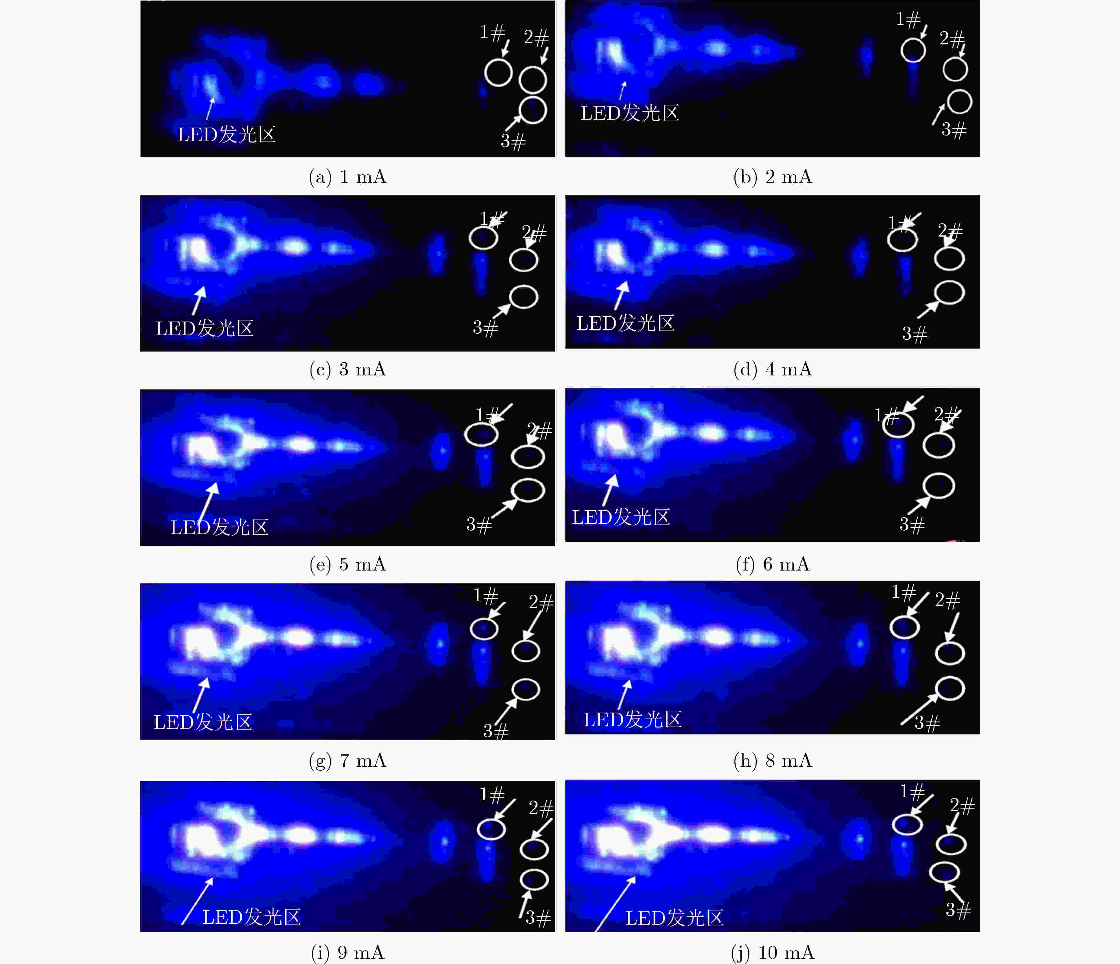
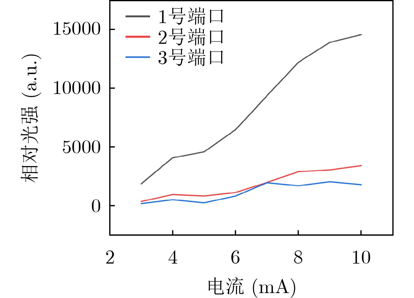
摘要: 为研究面向可见光通信的多功能光子集成芯片,实现可见光信号发射、探测、传输和功率分配的一体化的复合功能,该文提出一种基于硅基InGaN/GaN多量子阱材料的微型发光二极管(LED)多口分路器结构的光子集成芯片,对集成芯片进行了形貌、光电特性和可见光通信测试等多方面表征,实现了对可见光信号的有效传输和不同比例的多口功率分路,并对分路器不同端口的出射光强进行量化处理,最后,利用信号发生器在微型LED光源发射端加载300 kHz的矩形波电信号,收集分路器末端发射的调制可见光信号,输入/接收信号的波形变化趋势一致,说明该光子集成芯片可实现有效的可见光通信。该研究的主要目的是尝试性将可见光波段的光源和光电探测器集成在氮化物晶圆上,为可见光通信的全光网络的可见光信号片上集成式处理提供新的研究思路和方案,为发展面向可见光通信网络需求的复合功能光子集成芯片终端提供了更多可能性。Abstract: In order to study the multi-functional photon integrated chip for visible light communication and realize the integrated function of visible light signal emission, detection, transmission and power distribution, a miniature Light Emitting Diode(LED) with splitter structure based on silicon-based InGaN/GaN multiple quantum well material is proposed in this paper. The photon integrated chip is characterized in many aspects, such as morphology, optoelectronic characteristics and visible light communication test. The effective transmission of visible light signal and different proportion of multi-port power shunt are realized, and the output light intensity of different ports of the splitter is quantified. Finally, the rectangular wave signal of 300 kHz is loaded at the emitter end of the miniature LED light source by the signal generator, and the modulated visible light signal emitted at the end of the splitter is collected. The waveform change trend of the input / receive signal is the same. It shows that the photonic integrated chip can achieve effective visible light communication. The main purpose of this study is to try to integrate visible light sources and photodetectors on nitride wafers, so as to provide new research ideas and schemes for on-chip integrated processing of visible light signals in all-optical networks of visible light communications. It provides more possibilities for the development of multi-function photon integrated chip terminals for visible light communication networks.
-
表 1 本研究与部分已发表光子集成芯片指标对比
表 2 分路器不同端口的出射光强
电流(mA) 3 4 5 6 7 8 9 10 1号端口光强(a.u.) 1854.1 4065.9 4580.9 6455.0 9363.0 12213.1 13929.8 14582.0 2号端口光强(a.u.) 330.1 922.0 797.9 1102.0 1964.0 2873.0 3021.0 3383.0 3号端口光强(a.u.) 147.1 481.0 215.1 795.9 1944.0 1684.0 2025.0 1776.0 -
[1] KUMARI M, SHEETAL A, and SHARMA R. Performance analysis of a full-duplex TWDM-PON using OFDM modulation with red LED visible light communication System[J]. Wireless Personal Communications, 2021, 119(3): 2539–2559. doi: 10.1007/s11277-021-08343-0 [2] KHALID A, RASHID F, TAHIR U, et al. Multi-carrier visible light communication system using enhanced sub-carrier index modulation and discrete wavelet transform[J/OL]. Wireless Personal Communications, 2021. [3] DAWOOD M A, SALEH S S, EL-BADAWY E S A, et al. A comparative analysis of localization algorithms for visible light communication[J]. Optical and Quantum Electronics, 2021, 53(2): 108. doi: 10.1007/s11082-021-02751-z [4] BEHRMAN K, FOUILIOUX J, IRELAND T, et al. 37-4: Micro LED defect analysis via photoluminescent and cathodoluminescent imaging[C]. SID Symposium Digest of Technical Papers, New York, USA, 2020: 532–535. [5] XIA Jiye, DONG Xiaobiao, YAO Zhibo, et al. Development of high-yield laser lift-off process for micro LED display[C]. SID Symposium Digest of Technical Papers, New York, USA, 2020: 55–57. [6] 王家先. 基于InP/ZnS量子点的全彩色Micro-LED陈列显示器件设计及制作研究[D]. [硕士论文], 中国科学院大学(中国科学院长春光学精密机械与物理研究所), 2020.WANG Jiaxian. Design and fabrication of full-color micro-LED array device based on InP/ZnS quantum dots material[D]. [Master dissertation], Changchun Institute of Optics, Fine Mechanics and Physics, Chinese Academy of Sciences, 2020. [7] ZHANG Shuailong, GONG Zheng, MCKENDRY J J D, et al. CMOS-controlled color-tunable smart display[J]. IEEE Photonics Journal, 2012, 4(5): 1639–1646. doi: 10.1109/JPHOT.2012.2212181 [8] TIAN Pengfei, MCKENDRY J J D, GONG Zheng, et al. Characteristics and applications of micro-pixelated GaN-based light emitting diodes on Si substrates[J]. Journal of Applied Physics, 2014, 115(3): 033112. doi: 10.1063/1.4862298 [9] ISLIM M S, FERREIRA R X, HE Xiangyu, et al. Towards 10 Gb/s orthogonal frequency division multiplexing-based visible light communication using a GaN violet micro-LED[J]. Photonics Research, 2017, 5(2): A35–A43. doi: 10.1364/PRJ.5.000A35 [10] PARK S I, BRENNER D S, SHIN G, et al. Soft, stretchable, fully implantable miniaturized optoelectronic systems for wireless optogenetics[J]. Nature Biotechnology, 2015, 33(12): 1280–1286. doi: 10.1038/nbt.3415 [11] GUILHABERT B, MASSOUBRE D, RICHARDSON E, et al. Sub-Micron lithography using InGaN micro-LEDs: Mask-free fabrication of LED arrays[J]. IEEE Photonics Technology Letters, 2012, 24(24): 2221–2224. doi: 10.1109/LPT.2012.2225612 [12] 梁栋, 谭庆贵, 蒋炜, 等. 面向下一代载荷系统应用的光子集成芯片探索[J]. 空间电子技术, 2020, 17(4): 126–131. doi: 10.3969/j.issn.1674-7135.2020.04.017LIANG Dong, TAN Qinggui, JIANG Wei, et al. Research on photonics integrated chips for future satellite payloads[J]. Space Electronic Technology, 2020, 17(4): 126–131. doi: 10.3969/j.issn.1674-7135.2020.04.017 [13] ALQULIAH A, ELKABBASH M, ZHANG Jihua, et al. Ultrabroadband, compact, polarization independent and efficient metasurface-based power splitter on lithium niobate waveguides[J]. Optics Express, 2021, 29(6): 8160–8170. doi: 10.1364/OE.415676 [14] YU Zejie, XI Xiang, MA Jingwen, et al. Photonic integrated circuits with bound states in the continuum[J]. Optica, 2019, 6(10): 1342–1348. doi: 10.1364/OPTICA.6.001342 [15] ZHANG Yan, DU Qingyang, WANG Chuangtang, et al. Monolithic integration of broadband optical isolators for polarization-diverse silicon photonics[J]. Optica, 2019, 6(4): 473–478. doi: 10.1364/OPTICA.6.000473 [16] 杨斌, 尹小杰, 李绍洋, 等. 二氧化硅平面光波导器件的研究进展[J]. 半导体光电, 2021, 42(2): 151–157,167. doi: 10.16818/j.issn1001-5868.2021.02.001YANG Bin, YIN Xiaojie, LI Shaoyang, et al. Recent progresses about silica-based planar lightwave circuit devices[J]. Semiconductor Optoelectronics, 2021, 42(2): 151–157,167. doi: 10.16818/j.issn1001-5868.2021.02.001 [17] 李勇奇, 蒋金宏, 余明芯, 等. 平面光波导光分路器耦合结构优化设计[J]. 光通信技术, 2019, 43(7): 9–13. doi: 10.13921/j.cnki.issn1002-5561.2019.07.003LI Yongqi, JIANG Jinhong, YU Mingxin, et al. Optimal design of the coupling structure of planar lightwave circuit optical splitter[J]. Optical Communication Technology, 2019, 43(7): 9–13. doi: 10.13921/j.cnki.issn1002-5561.2019.07.003 [18] BAI Yuping, HONG Yibo, ZHAO Quanbin, et al. Supersonic shear layer characteristics of two fluids with a splitter plate[J]. International Journal of Advanced Nuclear Reactor Design and Technology, 2021, 3: 1–10. doi: 10.1016/j.jandt.2021.03.001 [19] LIN Yucheng and CHEN Liangyü. Subtle application of electrical field-induced lossy mode resonance to enhance performance of optical planar waveguide biosensor[J]. Biosensors, 2021, 11(3): 86. doi: 10.3390/bios11030086 [20] GROMOVYI M, SEMOND F, DUBOZ J Y, et al. Low loss GaN waveguides for visible light on Si substrates[J]. Journal of the European Optical Society-Rapid Publications, 2014, 9: 14050. doi: 10.2971/jeos.2014.14050 [21] THUBTHIMTHONG B, SASAKI T, and HANE K. Asymmetrically and vertically coupled hybrid Si/GaN microring resonators for on-chip optical interconnects[J]. IEEE Photonics Journal, 2015, 7(4): 7801511. doi: 10.1109/JPHOT.2015.2464721 [22] 涂兴华, 倪彬, 杨烁, 等. 平面波导型1×4光分路器的优化设计[J]. 计算机应用, 2015, 35(S2): 24–26.TU Xinghua, NI Bin, YANG Shuo, et al. Optimization design of 1×4 planar lightware circuit splitter[J]. Journal of Computer Applications, 2015, 35(S2): 24–26. [23] 涂兴华, 耿胜各. 一种新型1×8平面波导光分路器的设计[J]. 量子电子学报, 2018, 35(1): 102–107. doi: 10.3969/j.issn.1007-5461.2018.01.016TU Xinghua and GENG Shengge. Design of a novel 1×8 optical power splitter based on planar waveguide[J]. Chinese Journal of Quantum Electronics, 2018, 35(1): 102–107. doi: 10.3969/j.issn.1007-5461.2018.01.016 [24] 尹小杰, 郑之远, 訾幸壮, 等. 基于Y型分支与布拉格光栅结构的集成光芯片研究[J]. 光子学报, 2021, 50(5): 0513002. doi: 10.3788/gzxb20215005.0513002YIN Xiaojie, ZHENG Zhiyuan, ZI Xingzhuang, et al. Integrated optical chip based on y-branch and Bragg grating structure[J]. Acta Photonica Sinica, 2021, 50(5): 0513002. doi: 10.3788/gzxb20215005.0513002 [25] TRIPATHY A K, TRIPATHY S K, and DAS S K. Multifunctional holographic gratings for simultaneous coupling and beam splitting applications in photonic integrated circuits[J]. International Journal of Information Technology, 2021, 13(1): 307–312. doi: 10.1007/s41870-020-00548-z [26] RAO D G S, SWARNAKAR S, and KUMAR S. Design of all-optical reversible logic gates using photonic crystal waveguides for optical computing and photonic integrated circuits[J]. Applied Optics, 2020, 59(35): 11003–11012. doi: 10.1364/AO.409404 -


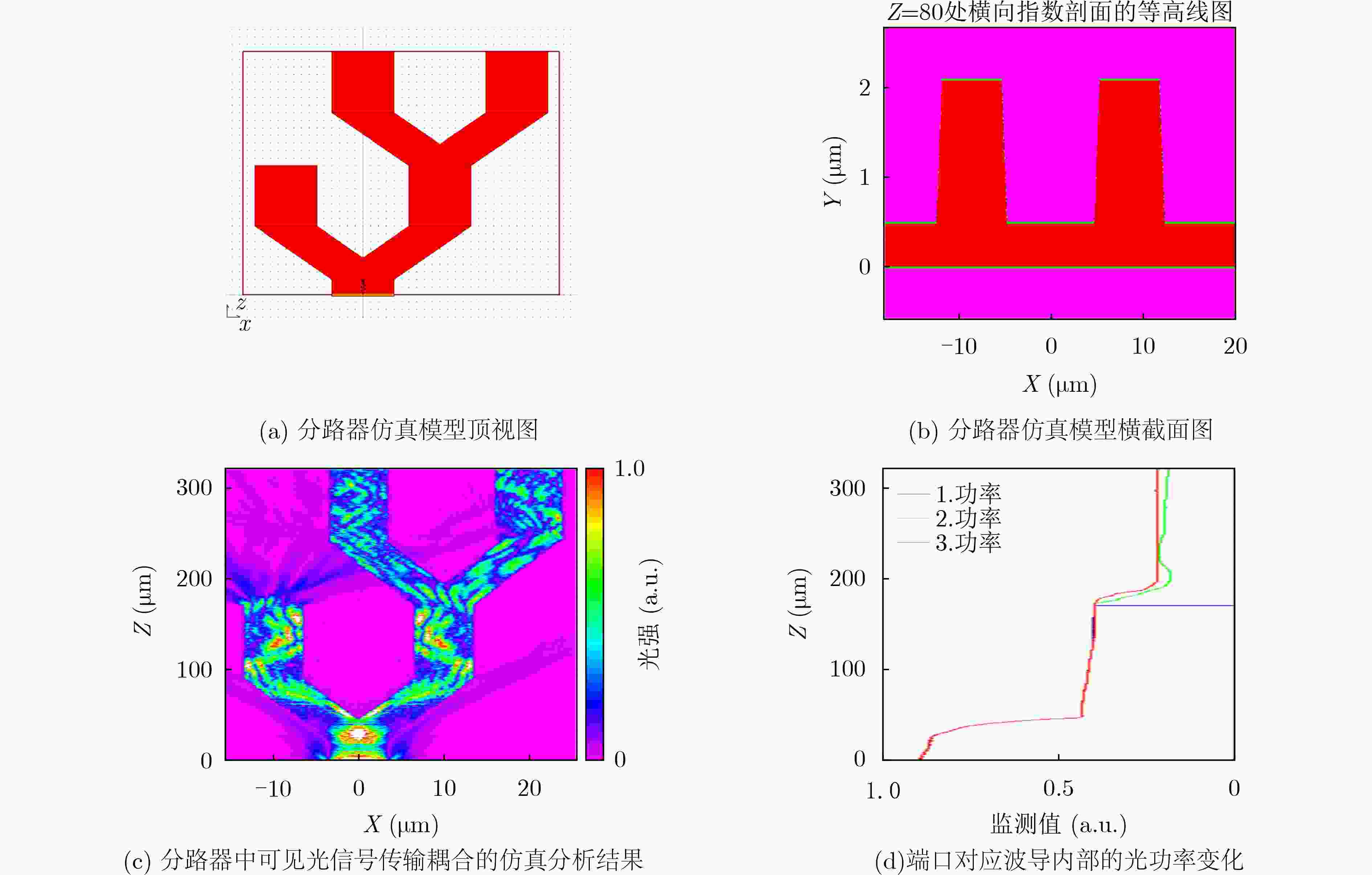
 下载:
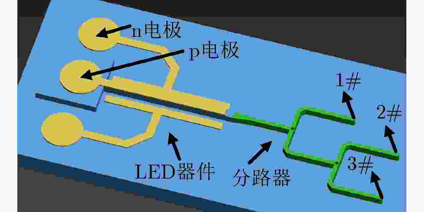
下载:


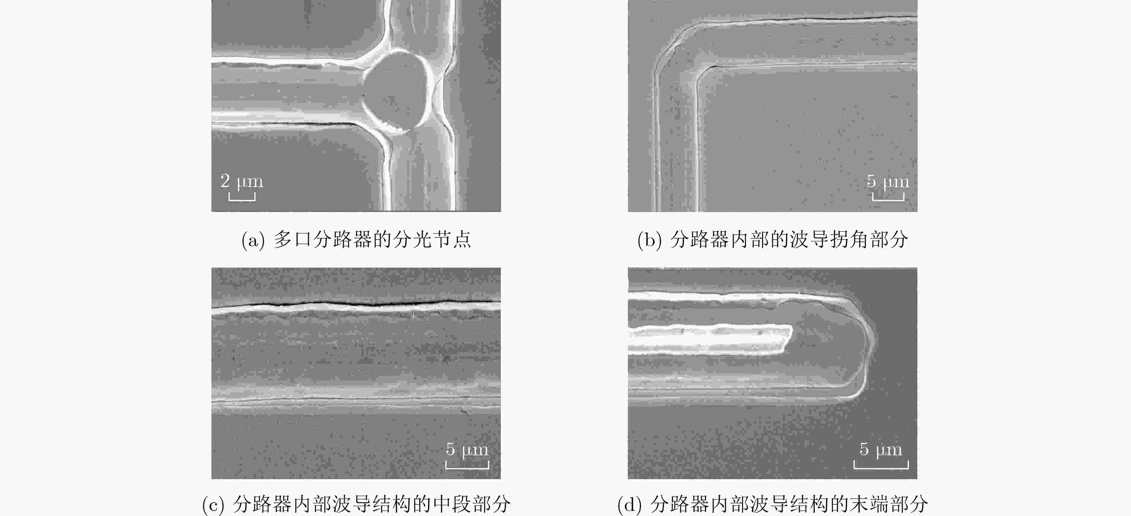



 下载:
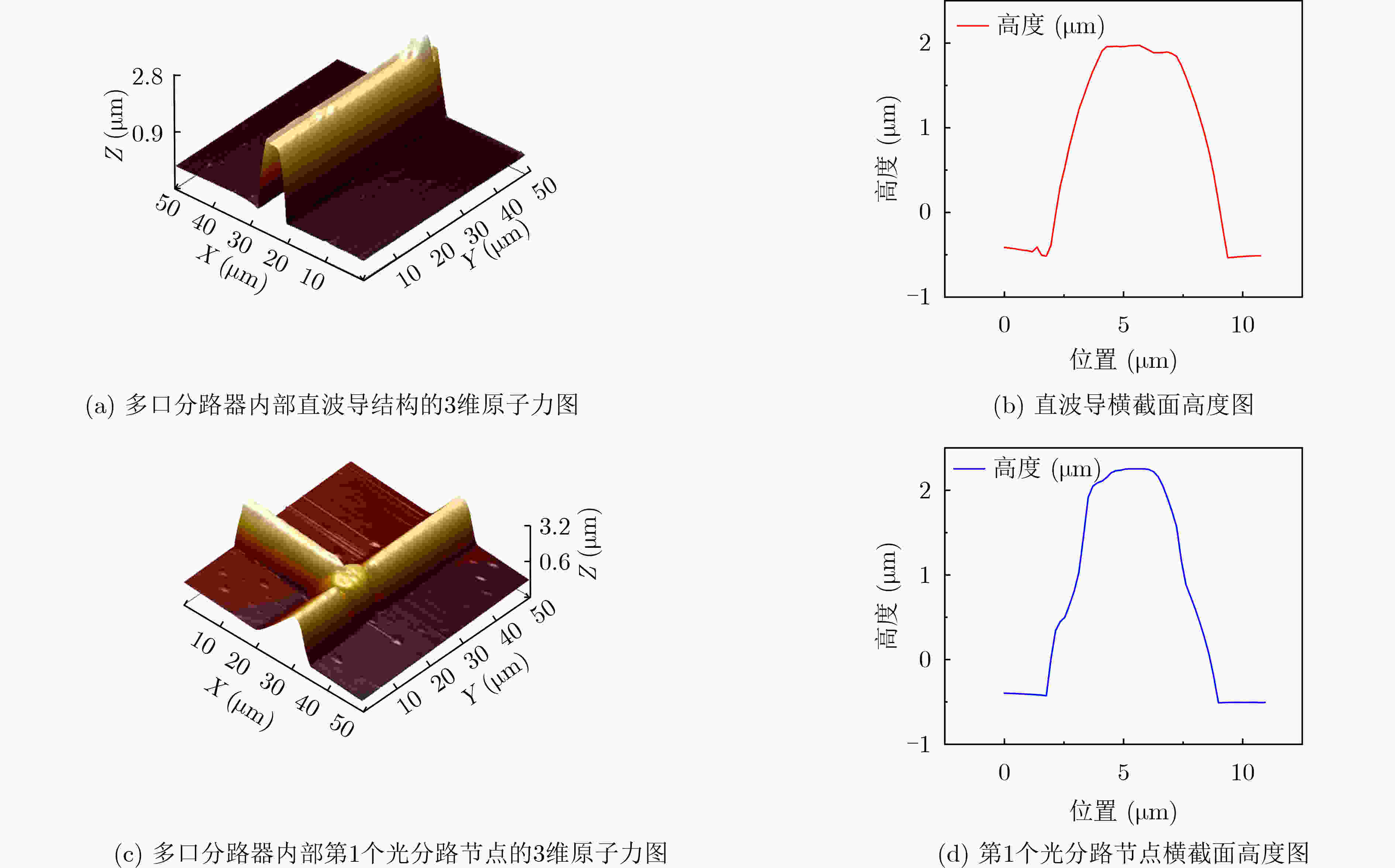
下载:
