

Co-design of Architecture and Packaging in Chiplet
-
摘要: 芯粒集成技术凭借封装集成的可扩展性,成为后摩尔时代算力拓展的有效途径。然而,芯粒集成芯片架构与封装的紧密耦合导致复杂的多目标权衡问题,同时体积集成密度的提高加剧了可靠性挑战,仅依靠封装层面设计难以解决,传统架构与封装分离的设计范式失效,架构-封装协同设计成为保障芯粒集成芯片性能与可靠性的必要手段。该工作总结芯粒集成驱动的新兴架构特征,梳理芯粒集成芯片架构与封装的紧密耦合关系,阐明协同设计的必要性;理清架构层与封装层核心设计要素对系统关键指标的影响机制,在此基础上定义架构层和封装层协同界面;最后结合已有工作提出架构-封装协同设计的关键组成和协同方法。Abstract:
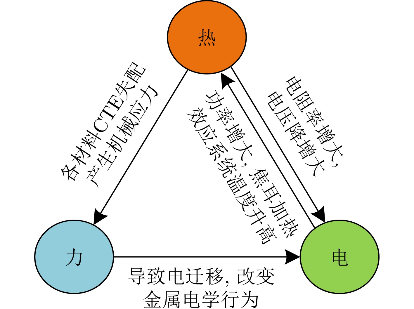
Significance Chiplet technology, enabled by advanced packaging techniques, integrates multiple chiplets into a single package to form a larger-scale chip system. This approach breaks through the “Area Wall” faced by traditional processes and has become a critical path for improving computing performance in the post-Moore era. The design flexibility afforded by packaging-level integration has created a new design paradigm that drives iterative advances in computing and integration architectures. In traditional monolithic chip design, architecture and packaging are relatively independent stages. By contrast, the ability to integrate chiplets fabricated in different processes and the scalability of chiplet technology greatly expand the design space but also increase design complexity. At the same time, the higher transistor density per unit volume intensifies multi-physics coupling effects, including thermal, mechanical, and electrical interactions. Therefore, traditional methods that rely solely on packaging design to address performance degradation and reliability issues are no longer sufficient for chiplet-based systems. Instead, architecture and packaging in chiplet design must be co-designed in a coordinated manner. Progress This work addresses the critical issues of architecture-packaging co-design in the context of chiplet systems. It reviews architectural design and co-optimization efforts, demonstrates the necessity of co-design, and proposes co-design optimization methodologies. First, it summarizes architectural characteristics and development trends driven by advanced packaging technologies. These technologies are categorized into 2D, 2.5D, 3D, and 3.5D integration according to chiplet arrangement and interconnection technologies, each leading to substantial architectural differences. A detailed comparison of packaging technologies is provided, outlining the architectural features and co-design considerations associated with each. The necessity of co-design is then clarified from the perspective of the profound effect of packaging technologies on performance and reliability. The increased integration density per unit volume in chiplet-based circuits introduces serious reliability challenges, including complex multi-physics coupling effects such as thermal, mechanical, and electrical interactions. Multiple research studies on chiplet reliability are cited, highlighting the severity of thermal, mechanical, and electrical problems arising from these couplings. Unlike traditional monolithic chip designs, reliability issues in chiplet-integrated circuits cannot be resolved through standalone packaging-level design. Separate design of architecture and packaging introduces performance risks and leads to unpredictable design and manufacturing timelines and costs. Therefore, co-design of architecture and packaging is a necessary trend for the advancement of chiplet-based circuits. Finally, by reviewing existing cross-layer co-optimization efforts, an architecture-packaging co-optimization methodology is proposed to provide guidance for design optimization. Key design factors and evaluation metrics at both the architectural and packaging levels are summarized, and the interfaces for cross-layer co-design are clarified. The co-design interface consists of two components: design factors and evaluation metrics. Adjustments to any design factor within the design space affect multiple evaluation metrics, which in turn drive the convergence of the design space. Two key components are summarized for each design layer: (1) the definition of the design parameter space and exploration methods, and (2) the selection of evaluation metrics together with evaluation models and methodologies. The co-design process is outlined in eight key steps, illustrated by prior works. Existing architecture-packaging co-design methods are reviewed, and design workflows are categorized and characterized. Conclusions Driven by the evolution of chiplet technology and objectives such as performance and cost, chiplet-integrated circuit architectures have developed characteristics that differentiate them from traditional monolithic designs. The strong coupling between architecture and packaging layers has substantially increased design complexity, while higher integration density has introduced intricate multi-physics interactions, elevating reliability risks. The traditional design paradigm, in which architecture and packaging are developed independently, now faces challenges including performance degradation, unpredictable verification timelines, and uncontrollable costs. Co-design has therefore emerged as a critical solution. Establishing cross-layer collaborative methods and making trade-offs among multidimensional objectives are essential. By defining the design spaces for both architecture and packaging, formulating efficient exploration strategies, and applying system- and packaging-level evaluation methods, it becomes possible to rapidly and accurately identify optimal design solutions. Architecture-packaging co-design enables performance, reliability, and other objectives to be optimized synergistically at the early stages of chiplet-integrated circuit design with minimal cost. This approach maximizes the benefits of high integration density while mitigating risks in chip design and manufacturing. Prospects Architecture-packaging co-design represents the future paradigm for chiplet design. Current co-design approaches remain limited in applicability: methods that rely on detailed models such as RTL and netlists, together with EDA tools, are unsuitable for early-stage chip development, whereas abstract modeling techniques may neglect critical design issues and introduce substantial inaccuracies. Future co-design methodologies must adapt to different stages of the design process and support the iterative advancement of both computing architectures and integration architectures. -
Key words:
- Chiplet /
- Co-design /
- Architecture /
- Packaging
-
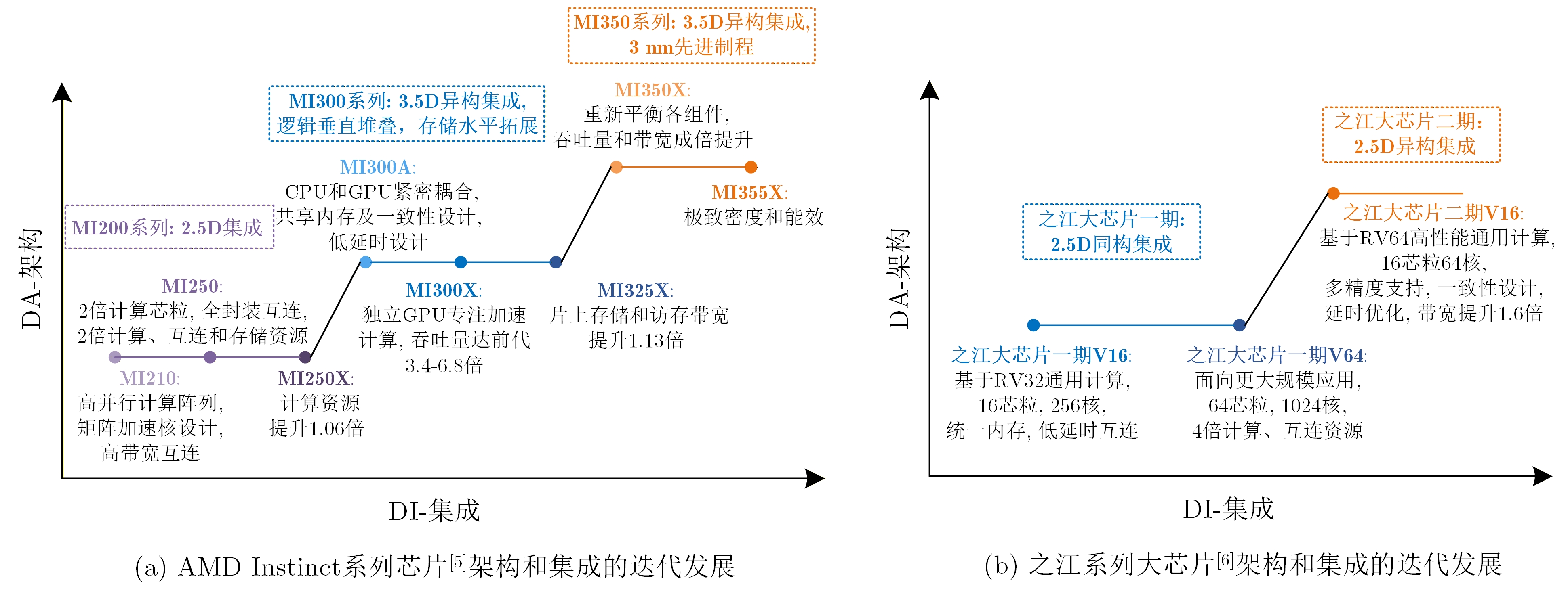
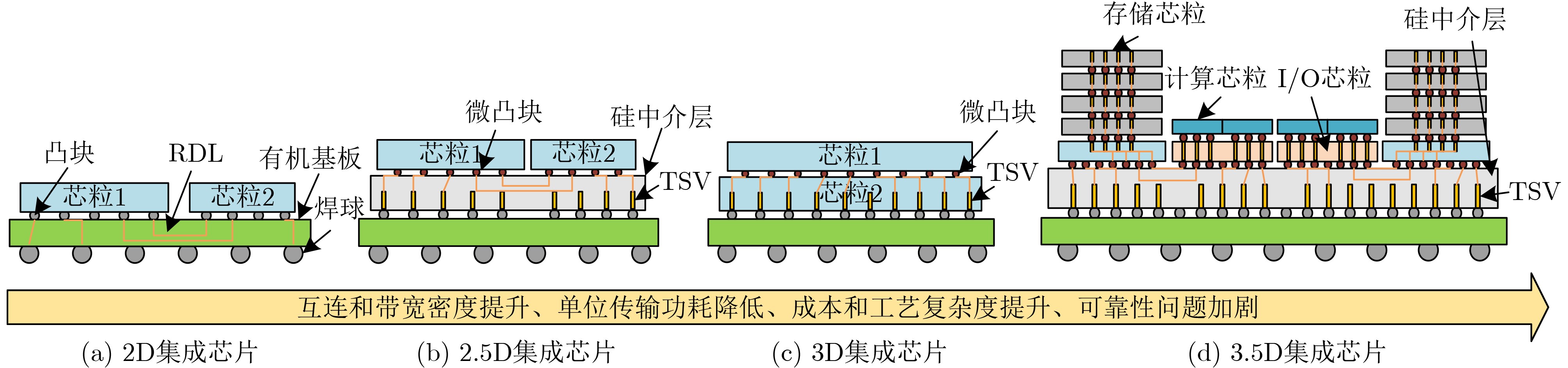
表 1 芯粒集成技术对比与典型芯片
集成
方式特点 主要参数 典型芯片 线距
(μm)凸块间距
(μm)功耗
(pJ/bit)归一化
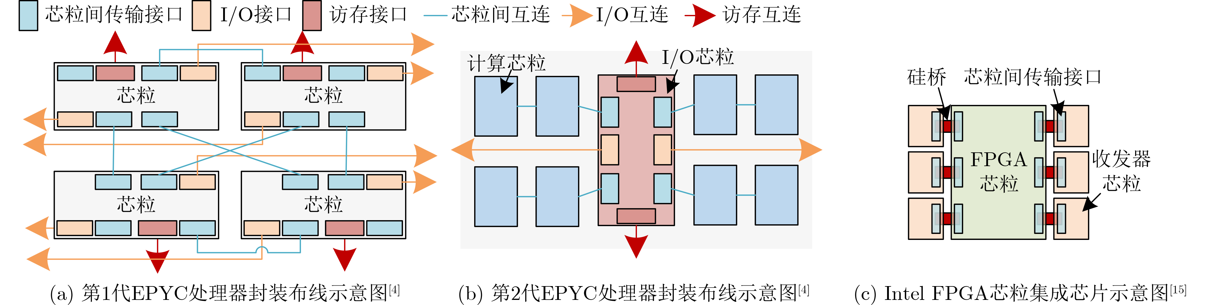
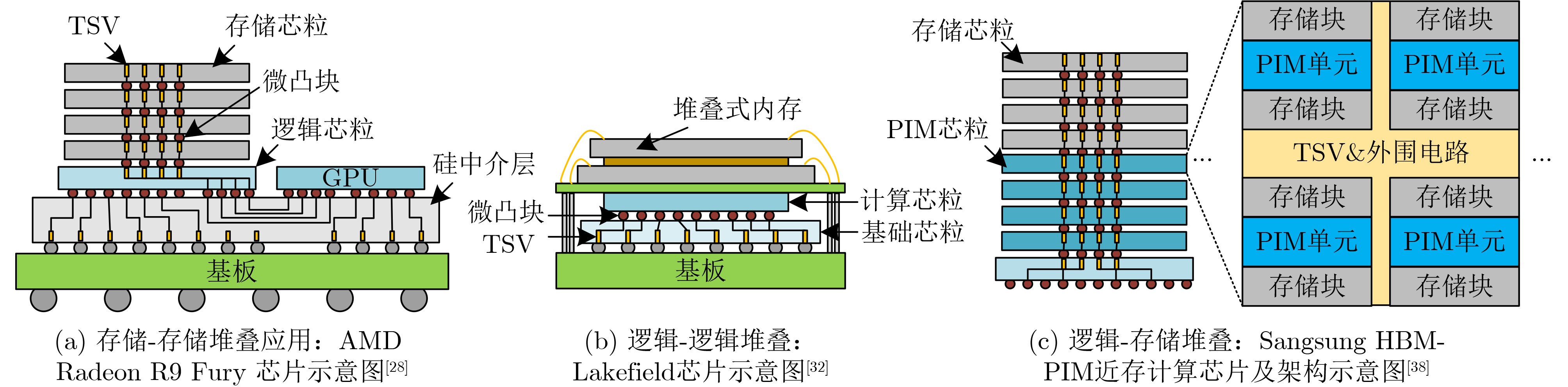
成本2D 有机基板互连。成本低,可靠性高,面积扩展性好;互连密度低 ~10 ~100 ~1.7 1 AMD EPYCTM, RyzenTM [4], Nvidia Simba [11] 2.5D 硅等中介层互连。互连密度较高;面积受限,成本高,可靠性问题 <4 ~50 ~0.5 1.5~(>3)[9] Instinct MI200 series[5], Intel FGPA[15], 华为Kunpeng 920[16], Intel Meteor Lake[17], Intel Sapphire Rapids(SPR)[18], Occamy[19], Manticore[20], Centaur[21], AMD RadeonTM R9 Fury X[28] 3D 垂直堆叠,硅通孔互连。互连密度高,延时、功耗低;成本高,可靠性问题显著 <2 ~40 ~0.15 >3[9,26,27] IntAct[14], HBM[25](商用芯片常见[29–31]), Intel Lakefield[32], SHINSAI[33], Lu等人[34], 华为 Ascend910[35], AMD V-Cache[36], Niu等人[37], Samsung HBM2-PIM[38] 3.5D 2.5D和3D结合。水平垂直互连协同设计,灵活性强;成本高,可靠性问题显著 <1 ~40 <0.1 >3[42] Intel PVC[43], AMD InstinctTM
MI300 series [41,44] 下载: 导出CSV
表 2 典型架构封装协同设计工作设计空间探索方法总结
协同方法组成 分类 细分类型或使用范围 典型工作(及算法) 设计空间描述 参数和功能模型 - 文献[56,58,62,64,66,68,69] 详细设计描述文件 - 文献[51,57,63,67] 空间探索方法 有限设计点 架构层 文献[55,62,56,64,66,68] 封装层 文献[64,68] 迭代优化 架构层功能级分解组合 文献[58,69](启发式),文献[56](数学建模法) 架构层网表级分解组合 文献[51,57,67](启发式),文献[63](数学建模法) 封装层 文献[51,56,58,62,63,69](启发式),
文献[57,62,66,67](数学建模法)评估指标 可靠性考量 热 文献[56,62,66] 力 文献[57,64,66,63] 电 文献[55,66–68] 无可靠性考量 - 文献[58,69] 评估方法 解析模型 系统级性能、面积、功耗、成本等 文献[56–58,62,64,69] 封装层时序、温度、应力 文献[57–58,62] 模拟模型 系统级性能、面积、功耗、成本等 文献[56,57,62–64,66,67,69] 封装层时序、温度 文献[51,56,62,63,66–68]
下载: 导出CSV
-
[1] ESMAEILZADEH H, BLEM E, AMANT R S, et al. Dark silicon and the end of multicore scaling[C]. The 2011 38th Annual International Symposium on Computer Architecture, San Jose, USA, 2011: 365–376. [2] HRUSKA J. As chip design costs skyrocket, 3nm process node is in jeopardy[EB/OL]. https://www.extremetech.com/computing/272096-3nm-process-node, 2018. [3] LAU J H. Semiconductor Advanced Packaging[M]. Singapore: Springer, 2021: 1–25. doi: 10.1007/978-981-16-1376-0. [4] NAFFZIGER S, BECK N, BURD T, et al. Pioneering chiplet technology and design for the AMD EPYC™ and Ryzen™ processor families: Industrial product[C]. The 2021 ACM/IEEE 48th Annual International Symposium on Computer Architecture (ISCA), Valencia, Spain, 2021: 57–70. doi: 10.1109/ISCA52012.2021.00014. [5] AMD. AMD instinct™ GPUs[EB/OL]. https://www.amd.com/en/products/accelerators/instinct.html, 2025. [6] HAN Yinhe, XU Haobo, LU Meixuan, et al. The big chip: Challenge, model and architecture[J]. Fundamental Research, 2024, 4(6): 1431–1441. doi: 10.1016/j.fmre.2023.10.020. [7] Intel. Tick/tock development model[EB/OL]. https://retailedge.intel.com/content/pdf/asmo/201303art_computerpoweruser.pdf, 2025. [8] WONG C P and WONG M M. Recent advances in plastic packaging of flip-chip and MultiChip Modules (MCM) of microelectronics[J]. IEEE Transactions on Components and Packaging Technologies, 1999, 22(1): 21–25. doi: 10.1109/6144.759349. [9] RADOJCIC R. More-Than-Moore 2.5D and 3D SiP Integration[M]. Cham: Springer, 2017. [10] SHEIKH F, NAGISETTY R, KARNIK T, et al. 2.5 D and 3D heterogeneous integration: Emerging applications[J]. IEEE Solid-State Circuits Magazine, 2021, 13(4): 77–87. doi: 10.1109/MSSC.2021.3111386. [11] ZIMMER B, VENKATESAN R, SHAO Y S, et al. A 0.32–128 TOPS, scalable multi-chip-module-based deep neural network inference accelerator with ground-referenced signaling in 16 nm[J]. IEEE Journal of Solid-State Circuits, 2020, 55(4): 920–932. doi: 10.1109/JSSC.2019.2960488. [12] MAHAJAN R, SANKMAN R, PATEL N, et al. Embedded multi-die interconnect bridge (EMIB)--a high density, high bandwidth packaging interconnect[C]. The 2016 IEEE 66th Electronic Components and Technology Conference (ECTC), Las Vegas, USA, 2016: 557–565. doi: 10.1109/ECTC.2016.201. [13] CHEN W C, HU C, TING K C, et al. Wafer level integration of an advanced logic-memory system through 2nd generation CoWoS® technology[C]. The 2017 Symposium on VLSI Technology, Kyoto, Japan, 2017: T54–T55. doi: 10.23919/VLSIT.2017.7998198. [14] VIVET P, GUTHMULLER E, THONNART Y, et al. IntAct: A 96-core processor with six chiplets 3D-stacked on an active interposer with distributed interconnects and integrated power management[J]. IEEE Journal of Solid-State Circuits, 2021, 56(1): 79–97. doi: 10.1109/JSSC.2020.3036341. [15] GREENHILL D, HO R, LEWIS D, et al. 3.3 A 14nm 1GHz FPGA with 2.5D transceiver integration[C]. The 2017 IEEE International Solid-State Circuits Conference (ISSCC), San Francisco, USA, 2017: 54–55. doi: 10.1109/ISSCC.2017.7870257. [16] XIA Jing, CHENG Chuanning, ZHOU Xiping, et al. Kunpeng 920: The first 7-nm chiplet-based 64-core ARM SoC for cloud services[J]. IEEE Micro, 2021, 41(5): 67–75. doi: 10.1109/MM.2021.3085578. [17] GOMES W, MORGAN S, PHELPS B, et al. Meteor lake and arrow lake Intel next-gen 3D client architecture platform with foveros[C]. The 2022 IEEE Hot Chips 34 Symposium (HCS), Cupertino, USA, 2022: 1–40. doi: 10.1109/HCS55958.2022.9895532. [18] NASSIF N, MUNCH A O, MOLNAR C L, et al. Sapphire rapids: The next-generation Intel Xeon scalable processor[C]. The 2022 IEEE International Solid-State Circuits Conference (ISSCC), San Francisco, USA, 2022: 44–46. doi: 10.1109/ISSCC42614.2022.9731107. [19] SCHEFFLER P, BENZ T, POTOCNIK V, et al. Occamy: A 432-core dual-chiplet dual-HBM2E 768-DP-GFLOP/s RISC-V system for 8-to-64-bit dense and sparse computing in 12-nm FinFET[J]. IEEE Journal of Solid-State Circuits, 2025, 60(4): 1324–1338. doi: 10.1109/JSSC.2025.3529249. [20] ZARUBA F, SCHUIKI F, and BENINI L. Manticore: A 4096-core RISC-V chiplet architecture for ultraefficient floating-point computing[J]. IEEE Micro, 2021, 41(2): 36–42. doi: 10.1109/MM.2020.3045564. [21] HWANG R, KIM T, KWON Y, et al. Centaur: A chiplet-based, hybrid sparse-dense accelerator for personalized recommendations[C]. The 2020 ACM/IEEE 47th Annual International Symposium on Computer Architecture (ISCA), Valencia, Spain, 2020: 968–981. doi: 10.1109/ISCA45697.2020.00083. [22] ZHOU Minghao, LI Li, HOU Fengze, et al. Thermal modeling of a chiplet-based packaging with a 2.5-D through-silicon via interposer[J]. IEEE Transactions on Components, Packaging and Manufacturing Technology, 2022, 12(6): 956–963. doi: 10.1109/TCPMT.2022.3174608. [23] ZHANG Yang, SARVEY T E, and BAKIR M S. Thermal evaluation of 2.5-D integration using bridge-chip technology: Challenges and opportunities[J]. IEEE Transactions on Components, Packaging and Manufacturing Technology, 2017, 7(7): 1101–1110. doi: 10.1109/TCPMT.2017.2710042. [24] INGERLY D B, AMIN S, ARYASOMAYAJULA L, et al. Foveros: 3D integration and the use of face-to-face chip stacking for logic devices[C]. The 2019 IEEE International Electron Devices Meeting (IEDM), San Francisco, USA, 2019: 19.6. 1–19.6. 4. doi: 10.1109/IEDM19573.2019.8993637. [25] SK hynix. Ultimate DRAM for new horizons of high-end memory[EB/OL]. https://product.skhynix.com/products/dram/hbm/hbm3.go, 2025. [26] STOW D, AKGUN I, BARNES R, et al. Cost and thermal analysis of high-performance 2.5D and 3D integrated circuit design space[C]. The 2016 IEEE Computer Society Annual Symposium on VLSI (ISVLSI), Pittsburgh, USA, 2016: 637–642. doi: 10.1109/ISVLSI.2016.133. [27] VELENIS D, DETALLE M, CIVALE Y, et al. Cost comparison between 3D and 2.5D integration[C]. The 2012 4th Electronic System-Integration Technology Conference, Amsterdam, Netherlands, 2012: 1–4. doi: 10.1109/ESTC.2012.6542130. [28] MACRI J. AMD's next generation GPU and high bandwidth memory architecture: FURY[C]. The 2015 IEEE Hot Chips 27 Symposium (HCS), Cupertino, USA, 2015: 1–26. doi: 10.1109/HOTCHIPS.2015.7477461. [29] NVIDIA. NVIDIA tesla V100[EB/OL]. https://www.nvidia.com/en-gb/data-center/tesla-v100/, 2025. [30] NVIDIA. NVIDIA A100 tensor core GPU[EB/OL]. https://www.nvidia.com/en-us/data-center/a100/, 2020. [31] NVIDIA. NVIDIA H100 tensor core GPU[EB/OL]. https://www.nvidia.com/en-us/data-center/h100/, 2020. [32] GOMES W, KHUSHU S, INGERLY D B, et al. 8.1 Lakefield and mobility compute: A 3D stacked 10nm and 22FFL hybrid processor system in 12×12mm2, 1mm package-on-package[C]. The 2020 IEEE International Solid-State Circuits Conference-(ISSCC), San Francisco, USA, 2020: 144–146. doi: 10.1109/ISSCC19947.2020.9062957. [33] JIAO Bo, ZHU Haozhe, ZENG Yuman, et al. 37.4 SHINSAI: A 586mm2 reusable active TSV interposer with programmable interconnect fabric and 512Mb 3D underdeck memory[C]. The 2025 IEEE International Solid-State Circuits Conference (ISSCC), San Francisco, USA, 2025, 68: 1–3. doi: 10.1109/ISSCC49661.2025.10904819. [34] LU Wei, ZHANG Jie, WEI Yihui, et al. Scalable Embedded Multi-Die Active Bridge (S-EMAB) chips with integrated LDOs for low-cost programmable 2.5D/3.5D packaging technology[C]. The 2024 IEEE Symposium on VLSI Technology and Circuits (VLSI Technology and Circuits), Honolulu, USA, 2024: 1–2. doi: 10.1109/VLSITechnologyandCir46783.2024.10631526. [35] LIAO Heng, TU Jiajin, XIA Jing, et al. Ascend: A scalable and unified architecture for ubiquitous deep neural network computing: Industry track paper[C]. The 2021 IEEE International Symposium on High-Performance Computer Architecture (HPCA), Seoul, Korea, 2021: 789–801. doi: 10.1109/HPCA51647.2021.00071. [36] WUU J, AGARWAL R, CIRAULA M, et al. 3D V-cache: The implementation of a hybrid-bonded 64MB stacked cache for a 7nm x86–64 CPU[C]. The 2022 IEEE International Solid-State Circuits Conference (ISSCC), San Francisco, USA, 2022: 428–429. doi: 10.1109/ISSCC42614.2022.9731565. [37] NIU Dimin, LI Shuangchen, WANG Yuhao, et al. 184QPS/W 64Mb/mm23D logic-to-DRAM hybrid bonding with process-near-memory engine for recommendation system[C]. Proceedings of the 2022 IEEE International Solid-State Circuits Conference (ISSCC), San Francisco, USA, 2022, 65: 1–3. doi: 10.1109/ISSCC42614.2022.9731694. [38] KIM J H, KANG S H, LEE S, et al. Aquabolt-XL: Samsung HBM2-PIM with in-memory processing for ML accelerators and beyond[C]. The 2021 IEEE Hot Chips 33 Symposium (HCS), Palo Alto, USA, 2021: 1–26. doi: 10.1109/HCS52781.2021.9567191. [39] FANG E J W, SHIH T C J, and HUANG D S Y. IR to routing challenge and solution for interposer-based design[C]. The 20th Asia and South Pacific Design Automation Conference, Chiba, Japan, 2015: 226–230. doi: 10.1109/ASPDAC.2015.7059009. [40] LEE I, NAM S, KIM S, et al. Extremely large 3.5D heterogeneous integration for the next-generation packaging technology[C]. The 2023 IEEE 73rd Electronic Components and Technology Conference (ECTC), Orlando, USA, 2023: 893–898. doi: 10.1109/ECTC51909.2023.00154. [41] MANDALAPU C S, BUCH C, SHAH P, et al. 3.5D advanced packaging enabling heterogenous integration of HPC and AI accelerators[C]. The 2024 IEEE 74th Electronic Components and Technology Conference (ECTC), Denver, USA, 2024: 798–802. doi: 10.1109/ECTC51529.2024.00391. [42] BOBBA S, GAILLARDON P E, SEICULESCU C, et al. 3.5-D integration: A case study[C]. The 2013 IEEE International Symposium on Circuits and Systems (ISCAS), Beijing, China, 2013: 2087–2090. doi: 10.1109/ISCAS.2013.6572285. [43] GOMES W, KOKER A, STOVER P, et al. Ponte Vecchio: A multi-tile 3D stacked processor for exascale computing[C]. The 2022 IEEE International Solid-State Circuits Conference (ISSCC), San Francisco, USA, 2022: 42–44. doi: 10.1109/ISSCC42614.2022.9731673. [44] SMITH A, CHAPMAN E, PATEL C, et al. 11.1 AMD InstinctTM MI300 series modular chiplet package–HPC and AI accelerator for exa-class systems[C]. The 2024 IEEE International Solid-State Circuits Conference (ISSCC), San Francisco, USA, 2024, 67: 490–492. doi: 10.1109/ISSCC49657.2024.10454441. [45] JUNG M, PAN D Z, and LIM S K. Chip/package co-analysis of thermo-mechanical stress and reliability in TSV-based 3D ICs[C]. The 49th Annual Design Automation Conference, San Francisco, USA, 2012: 317–326. Doi: 10.1145/2228360.2228419. [46] MA Yenai, DELSHADTEHRANI L, DEMIRKIRAN C, et al. TAP-2.5D: A thermally-aware chiplet placement methodology for 2.5D systems[C]. The 2021 Design, Automation & Test in Europe Conference & Exhibition (DATE), Grenoble, France, 2021: 1246–1251. doi: 10.23919/DATE51398.2021.9474011. [47] HUANG Wei, GHOSH S, VELUSAMY S, et al. HotSpot: A compact thermal modeling methodology for early-stage VLSI design[J]. IEEE Transactions on Very Large Scale Integration (VLSI) Systems, 2006, 14(5): 501–513. doi: 10.1109/TVLSI.2006.876103. [48] MA Xiaoning, XU Qinzhi, WANG Chenghan, et al. An electrical-thermal co-simulation model of chiplet heterogeneous integration systems[J]. IEEE Transactions on Very Large Scale Integration (VLSI) Systems, 2024, 32(10): 1769–1781. doi: 10.1109/TVLSI.2024.3430498. [49] JUNG M, MITRA J, PAN D Z, et al. TSV stress-aware full-chip mechanical reliability analysis and optimization for 3D IC[C]. Proceedings of the 2011 48th ACM/EDAC/IEEE Design Automation Conference (DAC), San Diego, USA, 2011: 188–193. [50] SHIH M K, LAI Weihong, LIAO T, et al. Thermal and mechanical characterization of 2.5-D and fan-out chip on substrate chip-first and chip-last packages[J]. IEEE Transactions on Components, Packaging and Manufacturing Technology, 2022, 12(2): 297–305. doi: 10.1109/TCPMT.2022.3145377. [51] KABIR M D A, PETRANOVIC D, and PENG Yarui. Cross-boundary inductive timing optimization for 2.5D chiplet-package co-design[C/OL]. The 2021 Great Lakes Symposium on VLSI, 2021: 135–140. doi: 10.1145/3453688.3461505. [52] PAK J, PATHAK M, LIM S K, et al. Modeling of electromigration in through-silicon-via based 3D IC[C]. Proceedings of the 2011 IEEE 61st Electronic Components and Technology Conference (ECTC), Lake Buena Vista, USA, 2011: 1420–1427. doi: 10.1109/ECTC.2011.5898698. [53] KOTHARI G and GHOSE K. Thermally-aware multi-core chiplet stacking[C]. The 2023 IEEE/ACM International Conference on Computer Aided Design (ICCAD), San Francisco, USA, 2023: 1–9. doi: 10.1109/ICCAD57390.2023.10323991. [54] ERIS F, JOSHI A, KAHNG A B, et al. Leveraging thermally-aware chiplet organization in 2.5D systems to reclaim dark silicon[C]. The 2018 Design, Automation & Test in Europe Conference & Exhibition (DATE), Dresden, Germany, 2018: 1441–1446. doi: 10.23919/DATE.2018.8342238. [55] ZHI Changle, DONG Gang, YANG Deguang, et al. Electrical and thermal characteristics optimization in interposer-based 2.5-D integrated circuits[J]. IEEE Transactions on Very Large Scale Integration (VLSI) Systems, 2025, 33(3): 627–637. doi: 10.1109/TVLSI.2024.3478846. [56] LI Fuping, WANG Ying, CHENG Yuanqing, et al. GIA: A reusable general interposer architecture for agile chiplet integration[C]. The 41st IEEE/ACM International Conference on Computer-Aided Design, San Diego, USA, 2022: 42. doi: 10.1145/3508352.3549464. [57] CHEN Shixin, LI Shanyi, ZHUANG Zhen, et al. Floorplet: Performance-aware floorplan framework for chiplet integration[J]. IEEE Transactions on Computer-Aided Design of Integrated Circuits and Systems, 2024, 43(6): 1638–1649. doi: 10.1109/TCAD.2023.3347302. [58] LI Fuping, WANG Ying, WANG Yujie, et al. Chipletizer: Repartitioning SoCs for cost-effective chiplet integration[C]. The 2024 29th Asia and South Pacific Design Automation Conference (ASP-DAC), Incheon, South Korea, 2024: 58–64. doi: 10.1109/ASP-DAC58780.2024.10473888. [59] WANG Chenghan, XU Qinzhi, NIE Chuanjun, et al. An efficient thermal model of chiplet heterogeneous integration system for steady-state temperature prediction[J]. Microelectronics Reliability, 2023, 146: 115006. doi: 10.1016/j.microrel.2023.115006. [60] MALLYA N B, STRIKOS P, GOEL B, et al. A performance analysis of chiplet-based systems[C]. The 2025 Design, Automation & Test in Europe Conference (DATE), Lyon, France, 2025: 1–7. doi: 10.23919/DATE64628.2025.10992969. [61] NIE Chuanjun, XU Qinzhi, WANG Chenghan, et al. Efficient transient thermal analysis of chiplet heterogeneous integration[J]. Applied Thermal Engineering, 2023, 229: 120609. doi: 10.1016/j.applthermaleng.2023.120609. [62] COSKUN A, ERIS F, JOSHI A, et al. Cross-layer co-optimization of network design and chiplet placement in 2.5-D systems[J]. IEEE Transactions on Computer-Aided Design of Integrated Circuits and Systems, 2020, 39(12): 5183–5196. doi: 10.1109/TCAD.2020.2970019. [63] KABIR M D A and PENG Yarui. Chiplet-package co-design for 2.5D systems using standard ASIC CAD tools[C]. The 2020 25th Asia and South Pacific Design Automation Conference (ASP-DAC), Beijing, China, 2020: 351–356. doi: 10.1109/ASP-DAC47756.2020.9045734. [64] IFF P, BRUGGMANN B, BESTA M, et al. Rapidchiplet: A toolchain for rapid design space exploration of inter-chiplet interconnects[C]. The 22nd ACM International Conference on Computing Frontiers, Cagliari, Italy, 2025: 168–171. doi: 10.1145/3719276.3725170. [65] LI Fuping, WANG Ying, LU Meixuan, et al. The decomposition and combination paradigms of chiplet-based integrated chips[J]. Integrated Circuits and Systems, 2024, 1(1): 18–30. doi: 10.23919/ICS.2024.3451428. [66] PARK H, KIM J, CHEKURI V C K, et al. Design flow for active interposer-based 2.5-D ICs and study of RISC-V architecture with secure NoC[J]. IEEE Transactions on Components, Packaging and Manufacturing Technology, 2020, 10(12): 2047–2060. doi: 10.1109/TCPMT.2020.3033136. [67] KIM J, MURALI G, PARK H, et al. Architecture, chip, and package co-design flow for 2.5D IC design enabling heterogeneous IP reuse[C]. The 56th Annual Design Automation Conference, Las Vegas, USA, 2019: 178. doi: 10.1145/3316781.3317775. [68] NASRULLAH J, LUO Zhiquan, and TAYLOR G. Designing software configurable chips and SIPs using chiplets and zGlue[C]. The 52nd International Symposium on Microelectronics, Boston, USA, 2019: 27–32. doi: 10.4071/2380-4505-2019.1.000027. [69] IFF P, BRUGGMANN B, BESTA M, et al. PlaceIT: Placement-based inter-chiplet interconnect topologies[EB/OL]. https://arxiv.org/abs/2502.01449, 2025. -

 下载:
下载:


图(7) / 表(2)
计量
- 文章访问数: 1695
- HTML全文浏览量: 961
- PDF下载量: 235
- 被引次数: 0
