

A Probability-Based Parasitic Extraction Algorithm for Global-Routed VLSI Designs
-
摘要: 随着特征尺寸的不断缩小,寄生参数提取对于整体电路性能变得越来越重要。为了实现更快的设计收敛,该文提出一种基于概率的寄生参数提取算法,用于全局布线后的时序分析。通过一种新颖的基于网格的数据表示方法,该文开发了一种分区策略,以有效地捕获耦合导线段;然后构建了一个基于概率的平均模型,用于加速导线间距的计算;最后提出一种耦合效应感知的提取方法,以计算出精确的互连寄生参数。该文使用28 nm和7 nm技术节点下的工业电路评估所提出的算法。实验结果表明,所生成的寄生参数与领先的商业工具 Innovus具有强相关性,并且运行时间比Innovus快了21.6%。Abstract:
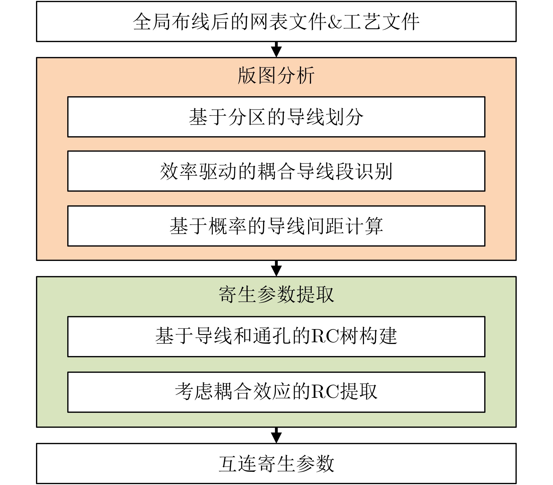
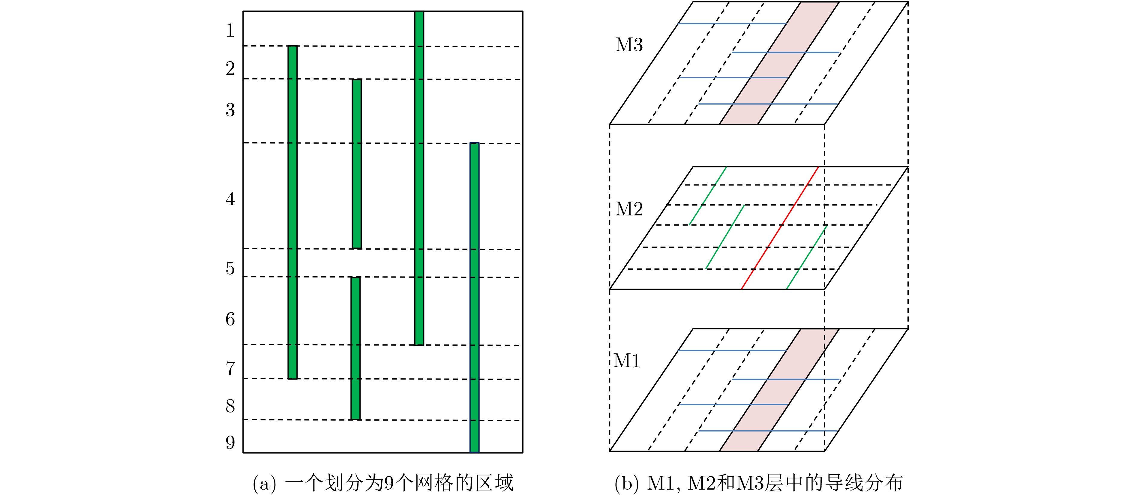
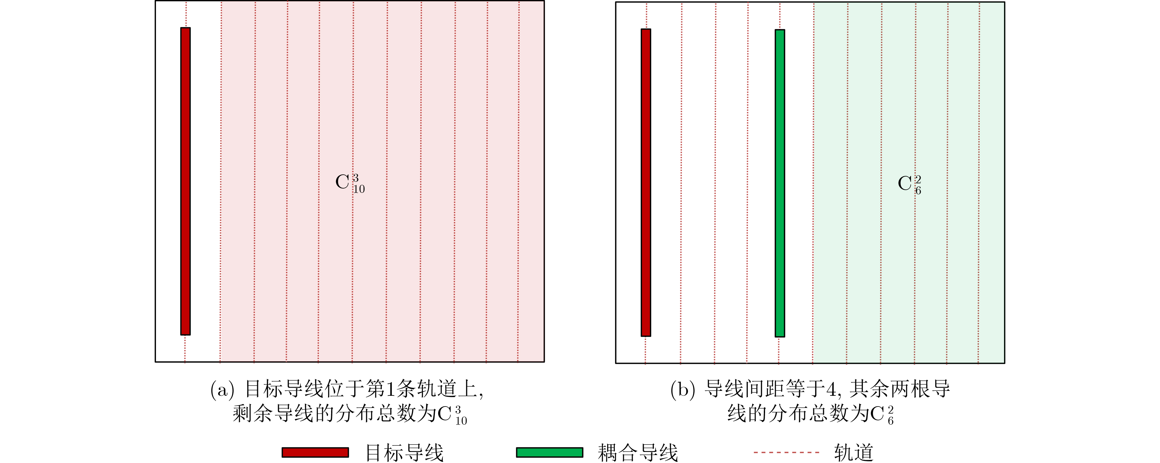
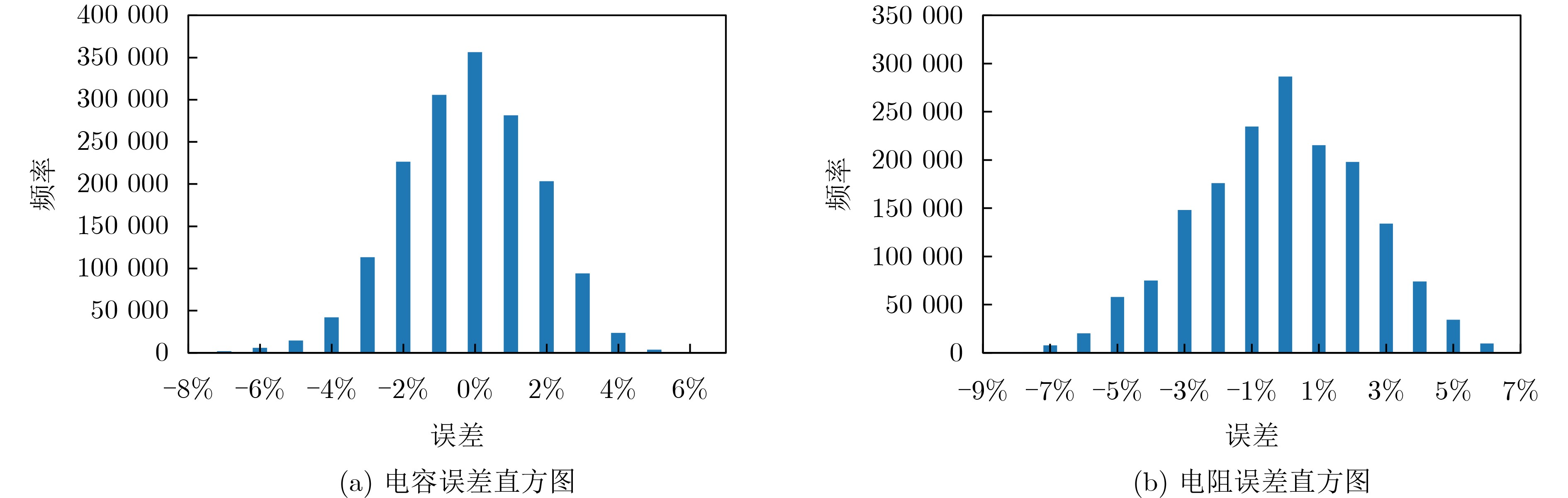
Objective Parasitic extraction is a critical stage in the VLSI design flow, as it determines the parasitic parameters of interconnect wires, directly affecting delay evaluation, timing analysis, and performance verification. With the increasing complexity of modern designs, accurate estimation of parasitic parameters has become a central challenge in routing. Developing a fast and accurate extraction algorithm is therefore essential to enable high-performance routing solutions. Methods Pattern matching is a widely used technique for full-layout parasitic extraction. Given an interconnect layout, the method divides it into small sections and determines the parasitics of each section with a pre-built pattern library. However, with billions of transistors placed on a single chip, the continuous growth of design complexity makes full-layout parasitic extraction increasingly challenging. Inspired by pattern matching, this paper presents a probability-based parasitic extraction algorithm tailored for modern VLSI designs. The proposed method consists of two main stages: (1) layout analysis and (2) parasitic extraction. Given a global-routed netlist and technology files containing pre-characterized parasitic values, layout analysis captures coupling segment information and generates a probability-based look-up table for efficient wire-spacing computation. Parasitic extraction then constructs the RC tree for each net and produces accurate interconnect parasitic parameters using the spacing information derived from layout analysis. For layout analysis, a partitioning strategy is employed to identify coupling segments that are parallel to and overlap with the target wire segment. In practice, coupling segments far from the target wire exert negligible effects on parasitics; therefore, the chip layout is divided into regions to improve identification efficiency. During parasitic extraction, coupling segments in both the same layer and in abutting layers are considered. If the target wire fully traverses the grids in an adjacent layer, all segments in those grids are treated as cross segments; otherwise, only partially overlapping segments are included. Once the coupling segments are determined, wire spacing must be calculated. In parasitic extraction, spacing represents the distance between a wire and its nearest neighbor. Because of the vast number of wires in modern circuits, computing exact spacing for every wire is prohibitively expensive. To address this, a probability-based average spacing model is proposed. In multilayer circuit designs, extraction also requires accurate reconstruction of routing information from layout data. In the standard Design Exchange Format (DEF), routing topology is represented by wires and vias. To handle this efficiently, a construction algorithm is developed to build connected RC trees from distributed wires and vias. Leveraging the probability-based wire-spacing model together with the technology files, the algorithm extracts parasitic parameters while accounting for coupling effects. The technology file “.captbl” provides interconnect parasitic tables indexed by wire width and spacing, with widths varying across different metal layers due to process constraints. Interpolation methods are first applied to obtain the unit resistance as a function of wire spacing and width. Wire resistance is then modeled by multiplying this unit resistance by wire length. Similarly, capacitance is extracted using interpolation, with additional coupling effects between neighboring layers captured through a grid-based recognition strategy that identifies the number of cross segments. Relative coupling capacitance is then determined accordingly. Results and Discussions Experiments were conducted on twelve industrial designs to evaluate the proposed extraction algorithm. The results demonstrate that the method achieves high parasitic accuracy while being 21.6% faster than the commercial tool Innovus. The average capacitance error is 1.15% with a standard deviation of 3.09%, and the average resistance error is 0.08% with a standard deviation of 2.63%. Notably, for all twelve circuits, the standard deviation of both capacitance and resistance errors remains below 5%. These findings confirm that the proposed algorithm provides both accuracy and efficiency for full-chip parasitic extraction, offering a practical foundation for developing high-performance routing algorithms. Conclusions This paper presents a probability-based parasitic extractor for addressing full-chip extraction challenges. A partitioning strategy with grid-based data representation is developed to capture coupling segments efficiently. Based on these segments, a probability-driven mathematical model is proposed to calculate wire spacing, with a pre-computed look-up table accelerating the computation. An efficient construction algorithm is further presented to build connected RC trees from distributed wires and vias, followed by a coupling-aware RC extraction method to produce accurate interconnect parasitics. Experimental evaluation on twelve industrial benchmarks demonstrates strong correlation between the extracted parasitics and those obtained from the commercial tool Innovus. -
Key words:
- Very large scale integration /
- Parasitic extraction /
- Timing analysis /
- Global routing
-
1 耦合导线段识别算法
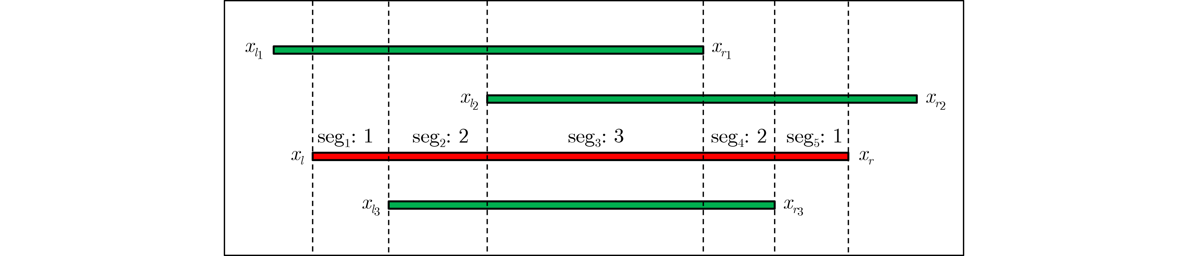
输入:导线$w$及其相邻信号线集合${\text{SR}}$ 输出:划分后的导线段集合$S$,包含耦合导线段的数量 (1) ${x_l}$,${x_r}$为$w$的起始和结束坐标 (2) $L$、$R$为${\text{SR}}$中信号线的起始和结束坐标集合 (3) $ U = L \cup R \cup {x_l} \cup {x_r} $ (4) ${\text{start}} = {x_l}$ (5) 将$L$, $R$, $U$按升序排序 (6) ${\text{seg\_num = getInitialSegNum()}}$ (7) while ${\text{start}} \ne \varnothing $ do (8) ${\text{end}} = U$中${\text{start}}$的下一个元素 (9) $S = S \cup \{ {\text{end,end-start,seg\_num}}\} $ (10) ${\text{start}} = {\text{end}}$ (11) if ${\text{start}} = = {x_r}$ then (12) break (13) else if ${\text{start}} \in L$ then (14) (${\text{seg\_num + + }}$ (15) else (16) ($ \mathrm{s}\mathrm{e}\mathrm{g}\_\mathrm{n}\mathrm{u}\mathrm{m}-- $ (17) end while (18) return $S$  下载: 导出CSV
2 基于导线和通孔的RC树构造
输入:导线集合$W$和通孔集合$V$ 输出:构造的RC树的节点集合$N$和边集合$E$ (1) $ {N}={\varnothing },\mathrm{ }\mathrm{ }\mathrm{ }\mathrm{ }\mathrm{ }\mathrm{ }{E}={\varnothing } $ (2) for $\{ {x_l},{y_b},{x_r},{y_t},{\text{layer}}\} $ in $W$ do (3) ${\text{nod}}{{\text{e}}_1} = {\text{get\_or\_create}}({x_l},{y_b},{\text{layer}})$ (4) ${\text{nod}}{{\text{e}}_2} = {\text{get\_or\_create}}({x_r},{y_t},{\text{layer}})$ (5) $ {\text{edge}} = {\text{create}}\_{\text{edge}}({\text{nod}}{{\text{e}}_1}{\text{,nod}}{{\text{e}}_2}) $ (6) $E = E \cup \{ {\text{edge}}\} $ (7) $N = N \cup \{ {\text{nod}}{{\text{e}}_1},{\text{nod}}{{\text{e}}_2}\} $ (8)end for (9)for $\{ x,y,{\text{lower\_layer}}\} $ in $V$ do (10) ${\text{vi}}{{\text{a}}_1} = {\text{get\_or\_create}}(x,y,{\text{lower\_layer}})$ (11) $ {\text{vi}}{{\text{a}}_2} = {\text{get\_or\_create}}(x,y,{\text{lower\_layer + 1}}) $ (12) $ {\text{edge}} = {\text{create}}\_{\text{edge}}({\text{vi}}{{\text{a}}_1}{\text{,vi}}{{\text{a}}_2}) $ (13) $E = E \cup \{ {\text{edge}}\} $ (14) $N = N \cup \{ {\text{vi}}{{\text{a}}_1},{\text{vi}}{{\text{a}}_2}\} $ (15) end for (16) 检查RC树的连通性 (17) return $N$, $E$
下载: 导出CSV
表 1 电容、电阻和运行时间与 Innovus 的比较
Benchmark Statistic Capacitance_error(%) Resistance_error(%) RT(s) Tech.(nm) #Stds #Nets Mean Std_dev Mean Std_dev 本文 Innovus HP_DEC_TOP 28 1657690 1672977 –0.19 1.32 –0.15 1.74 241 316 CPU_M0_WRAP 28 1021481 952813 –0.25 2.37 0.39 2.81 136 179 HPP_AHP 28 505021 518611 –0.09 4.95 0.18 2.57 80 99 HP_TOP_M1_VI 28 1512026 1612055 –0.15 3.81 0.01 1.86 256 296 M0_TPP 28 1457856 1610694 0.81 1.76 –0.43 1.57 227 288 MEDIA_SYSTEM 28 1050317 1116939 0.43 4.62 –0.29 1.74 158 189 MAQ_VI 7 2546138 1687508 1.72 2.98 –0.52 2.73 281 317 ROCKET_SUBSYS 7 2048857 1824439 4.13 3.07 0.47 4.36 260 319 RSFEC_fsu 7 2157315 1984282 1.52 4.44 1.05 4.50 321 363 MEDIA_iol 7 1058482 1023658 0.98 1.86 –0.42 4.19 151 190 HP_WRAP 7 2148977 2297812 1.15 2.34 –0.26 1.79 302 392 RX_SYSTEM_WRAP 7 4843973 4797617 3.59 4.90 0.74 3.41 793 847 Average 1.15 3.09 0.08 2.63 1.000 1.216
下载: 导出CSV
表 2 Innovus没考虑NDR时与文章所提方法的对比
Benchmark Statistic Capacitance_error(%) Technology(nm) #Stds #Nets Mean Std_dev ROCKET_SUBSYS 7 2048857 1824439 1.35 2.41 RX_SYSTEM_WRAP 7 4843973 4797617 1.18 3.72
下载: 导出CSV
-
[1] SHI Hanyu and HE Qing. VLSI parasitic capacitance extraction based on pattern matching using modified machine learning methods[C]. The 10th International Conference on Computer and Communications (ICCC), Chengdu, China, 2024: 92–99. doi: 10.1109/ICCC62609.2024.10942273. [2] LIU Lihao, YANG Fan, SHANG Li, et al. GNN-cap: Chip-scale interconnect capacitance extraction using graph neural network[J]. IEEE Transactions on Computer-Aided Design of Integrated Circuits and Systems, 2024, 43(4): 1206–1217. doi: 10.1109/TCAD.2023.3331942. [3] PATIDAR S and BODADE R M. Evaluation trends and development in integrated circuit parasitic extraction[C]. 2024 IEEE International Students' Conference on Electrical, Electronics and Computer Science (SCEECS), Bhopal, India, 2024: 1–7. doi: 10.1109/SCEECS61402.2024.10482256. [4] ZEMANIAN A H. A finite-difference procedure for the exterior problem inherent in capacitance computations for VLSI interconnections[J]. IEEE Transactions on Electron Devices, 1988, 35(7): 985–992. doi: 10.1109/16.3355. [5] SUMANT P S and CANGELLARIS A C. Algebraic multigrid Laplace solver for the extraction of capacitances of conductors in multi-layer dielectrics[J]. International Journal of Numerical Modelling: Electronic Networks, Devices and Fields, 2007, 20(5): 253–269. doi: 10.1002/jnm.650. [6] YU Wenjian, SHEN Shan, YANG Dingcheng, et al. Deep learning inspired capacitance extraction techniques[C]. The 30th Asia and South Pacific Design Automation Conference, Tokyo, Japan, 2025: 106–112. doi: 10.1145/3658617.3703148. [7] WU Shengkun, XIE Biwei, and LI Xingquan. An adaptive partition strategy of Galerkin boundary element method for capacitance extraction[C]. The 28th Asia and South Pacific Design Automation Conference, Tokyo, Japan, 2023: 541–546. doi: 10.1145/3566097.3567903. [8] YU Wenjian, WANG Zeyi, and GU Jiangchun. Fast capacitance extraction of actual 3-D VLSI interconnects using quasi-multiple medium accelerated BEM[J]. IEEE Transactions on Microwave Theory and Techniques, 2003, 51(1): 109–119. doi: 10.1109/TMTT.2002.806923. [9] CHAI Wenwen, JIAO Dan, and KOH C K. A direct integral-equation solver of linear complexity for large-scale 3D capacitance and impedance extraction[C]. The 46th Annual Design Automation Conference, San Francisco, USA, 2009: 752–757. doi: 10.1145/1629911.1630107. [10] SHI Weiping, LIU Jianguo, KAKANI N, et al. A fast hierarchical algorithm for 3-D capacitance extraction[C]. The 35th Annual Design Automation Conference, San Francisco, USA, 1998: 212–217. doi: 10.1145/277044.277101. [11] YANG Ming and YU Wenjian. Floating random walk capacitance solver tackling conformal dielectric with on-the-fly sampling on eight-octant transition cubes[J]. IEEE Transactions on Computer-Aided Design of Integrated Circuits and Systems, 2020, 39(12): 4935–4943. doi: 10.1109/TCAD.2020.2968544. [12] YU Wenjian, ZHANG Bolong, ZHANG Chao, et al. Utilizing macromodels in floating random walk based capacitance extraction[C]. 2016 Design, Automation & Test in Europe Conference & Exhibition, Dresden, Germany, 2016: 1225–1230. [13] XU Jiahao, ZHANG Yibin, GAO Shenghan, et al. A 2-D multi-dielectric capacitance solver based on floating random walk method[C]. 2023 China Semiconductor Technology International Conference (CSTIC), Shanghai, China, 2023: 1–3. doi: 10.1109/CSTIC58779.2023.10219380. [14] WEI Xin, YAN Changhao, ZHOU Hai, et al. An efficient FPGA-based floating random walk solver for capacitance extraction using SDAccel[C]. 2019 Design, Automation & Test in Europe Conference & Exhibition, Florence, Italy, 2019: 1040–1045. doi: 1 0.23919/DATE.2019.8714992. [15] YU Wenjian, XU Zhezhao, LI Bo, et al. Floating random walk-based capacitance simulation considering general floating metals[J]. IEEE Transactions on Computer-Aided Design of Integrated Circuits and Systems, 2018, 37(8): 1711–1715. doi: 10.1109/TCAD.2017.2782770. [16] ARORA N D, RAOL K V, SCHUMANN R, et al. Modeling and extraction of interconnect capacitances for multilayer VLSI circuits[J]. IEEE Transactions on Computer-Aided Design of Integrated Circuits and Systems, 1996, 15(1): 58–67. doi: 10.1109/43.486272. [17] SAKURAI T and TAMARU K. Simple formulas for two- and three-dimensional capacitances[J]. IEEE Transactions on Electron Devices, 1983, 30(2): 183–185. doi: 10.1109/T-ED.1983.21093. [18] CHOUDHURY U and SANGIOVANNI-VINCENTELLI A L. Automatic generation of analytical models for interconnect capacitances[J]. IEEE Transactions on Computer-Aided Design of Integrated Circuits and Systems, 1995, 14(4): 470–480. doi: 10.1109/43.372374. [19] LI Zhixing and SHI Weiping. Layout capacitance extraction using automatic pre-characterization and machine learning[C]. 2020 21st International Symposium on Quality Electronic Design, Santa Clara, USA, 2020: 457–464. doi: 10.1109/ISQED48828.2020.9136970. [20] YANG Dingcheng, LI Haoyuan, YU Wenjian, et al. CNN-cap: Effective convolutional neural network-based capacitance models for interconnect capacitance extraction[J]. ACM Transactions on Design Automation of Electronic Systems, 2023, 28(4): 56. doi: 10.1145/3564931. [21] ABOUELYAZID M S, HAMMOUDA S, and ISMAIL Y. Accuracy-based hybrid parasitic capacitance extraction using rule-based, neural-networks, and field-solver methods[J]. IEEE Transactions on Computer-Aided Design of Integrated Circuits and Systems, 2022, 41(12): 5681–5694. doi: 10.1109/TCAD.2022.3161199. -

 下载:
下载:


图(6) / 表(4)
计量
- 文章访问数: 744
- HTML全文浏览量: 363
- PDF下载量: 46
- 被引次数: 0
