

Review of Research Progress on TSV Technology in 3D IC Packaging
-
摘要: 三维集成电路(3D IC)以其低延迟和高密度等优势,成为后摩尔时期的重要研究方向之一。其中硅通孔(TSV)作为3D IC中层间互连的关键技术,相关热、电和信号问题已有了广泛的研究。为更好地了解TSV技术的原理及研究现状,该文概述了近年来TSV技术在3D IC设计中的研究进展。首先,针对TSV热问题,综述了3D IC的热建模方法和TSV的热管理策略。其次,针对电源完整性问题,介绍了布局优化、背面供电网络(BPDN)技术等解决方案。之后,针对信号完整性问题,阐述了电磁屏蔽、应用低介电常数材料、新型互连等方法。最后,对TSV目前仍存在的局限性进行了总结,并在此基础上重点展望了多物理场协同优化、纳米级TSV(nTSV)与背面供电网络集成设计、新型材料与TSV阵列以及智能优化方法在未来的发展空间。Abstract:
Significance Three-Dimensional Integrated Circuits (3D ICs) have emerged as a key research direction in the post-Moore era due to their advantages in low latency and high integration density. As electronic devices demand higher performance and smaller form factors, 3D ICs offer a compelling solution by vertically stacking multiple chip layers to achieve enhanced integration. A core enabler of 3D IC technology is Through-Silicon Via (TSV) technology, which facilitates high-density vertical interconnects across layers. TSVs have contributed significantly to performance improvements in 3D ICs but also pose challenges in thermal management, power integrity, and signal integrity, all of which can affect device reliability and operational stability. Addressing these challenges is essential for the continued advancement of 3D IC systems. This review outlines recent research on TSV technology, with an emphasis on thermal, electrical, and signal integrity issues, as well as current strategies for mitigating these limitations. Progress This review systematically summarizes the progress in TSV technology, focusing on the following areas: Thermal Management: Thermal dissipation is a critical concern in 3D ICs due to elevated power densities resulting from multilayer stacking. While TSVs improve interconnect performance, they can also introduce vertical heat flow paths that lead to localized overheating and reduced reliability. To manage this, various thermal modeling approaches—such as Finite Element Analysis (FEA) and thermal stacking simulations, have been developed to predict temperature distributions and optimize thermal performance. These models inform the layout of TSVs and guide the incorporation of Thermal TSVs (TTSVs) to enhance heat dissipation. Researchers have also explored the use of high-thermal-conductivity materials, such as carbon nanotubes and graphene, to improve thermal pathways. Optimizing TSV density and employing multi-layer thermal redistribution techniques have further advanced thermal management, contributing to better device performance and longer operational lifetimes. Power Integrity: Power integrity is a major design constraint in 3D ICs, given the complex power delivery networks required in stacked architectures. TSVs, acting as vertical power conduits, can introduce issues such as voltage drops, electromigration, and power noise. Several approaches have been proposed to address these issues. Layout optimization—particularly through uniform TSV distribution and the integration of Backside Power Delivery Networks (BPDNs), helps reduce power delivery path lengths and mitigate voltage loss. Dynamic Voltage and Frequency Scaling (DVFS) is also employed to adapt power usage under varying workloads, particularly in high-performance computing environments. Additional methods include the use of Decoupling Capacitors (DECAPs) and Fully Integrated Voltage Regulators (FIVRs), which help suppress power noise and maintain stability across multiple voltage domains. Signal Integrity: TSV-based interconnects must maintain signal integrity at increasingly high frequencies, but parasitic inductance and capacitance inherent to TSVs can degrade signal quality through reflection, crosstalk, and delay mismatch. These effects become especially pronounced in high-density, high-speed interconnect architectures. To address this, electromagnetic shielding—using grounded TSVs and metallic isolation structures, has been shown to reduce crosstalk and enhance signal fidelity. The use of low-dielectric constant (low-ε) materials further minimizes parasitic capacitance and improves signal propagation speed. Differential TSV designs and advanced interconnect architectures have also been proposed to reduce interference and enhance signal integrity. These improvements are essential for achieving reliable high-speed data transmission in storage and processing applications. Conclusions While TSV technology has advanced substantially in addressing the thermal, power, and signal integrity challenges of 3D ICs, several limitations persist. These include scalability constraints, power delivery reliability under high-density integration, and diminished signal transmission quality at high frequencies. These challenges highlight the need for continued innovation in TSV design and integration to meet the demands of next-generation 3D IC systems. Several promising research directions are emerging. First, there is a growing need for higher-precision multiphysics coupling models. As 3D ICs progress toward large-scale heterogeneous integration, high-speed data communication, and extreme energy efficiency, more accurate modeling of the thermal, electrical, and signal interactions associated with TSVs is required. This calls for enhanced integration of multiphysics simulations into the Electronic Design Automation (EDA) workflow to enable co-simulation across electrical, thermal, and signal domains. Second, co-optimization of BPDNs and nano-TSVs (nTSVs) is becoming increasingly important. As chip dimensions decrease and stacking complexity grows, traditional front-side power delivery approaches no longer meet the required power densities. Improved BPDN strategies, in conjunction with nTSV integration, will support higher stacking capability and improved energy efficiency. Third, the exploration of new materials and TSV array structures offers additional opportunities. Carbon-based nanomaterials, used as TSV fillers or liners, can alleviate thermal expansion mismatch and improve resistance to electromigration. Incorporating air gaps or low-ε dielectrics as insulating liners can reduce parasitic capacitance and enhance high-speed signal performance. Meanwhile, novel TSV array architectures can increase interconnect density and improve redundancy and fault tolerance. Finally, the adoption of AI-driven TSV optimization holds considerable promise. TSV layout design currently depends heavily on manual heuristics. The application of artificial intelligence to automate TSV placement and power network distribution can significantly reduce design time and accelerate the transition toward more intelligent 3D integration design paradigms. -
表 1 不同TSV散热方案的性能优劣与适用范围
方案名称 参考文献 主要优势 主要劣势 适用场景 热再分布和热硅通
孔组成的冷却系统[28] 可以实现高效散热,工艺兼容性强 垂直散热依赖TTSV密度,横向散热受TRDL影响,热耦合效应未完全解决 移动设备与物联网芯片、
射频与光电集成碳材料基TSV [29] 具有超高导热系数,能显著提升垂直
散热效率,降低芯片温度,在高频
与高温环境下更稳定材料制备与集成难度大,成本高。界面热阻可能削弱整体散热效果 高性能计算与AI芯片、
航空航天与汽车电子调整TSV参数 [31]
[32]
[33]降低TSV周围热应力,减少热耦合,
节省芯片面积,系统性解决热问题增加制造复杂性,提高成本,需进一步考虑电性能与热性能的权衡 高功耗3D IC、对热应力
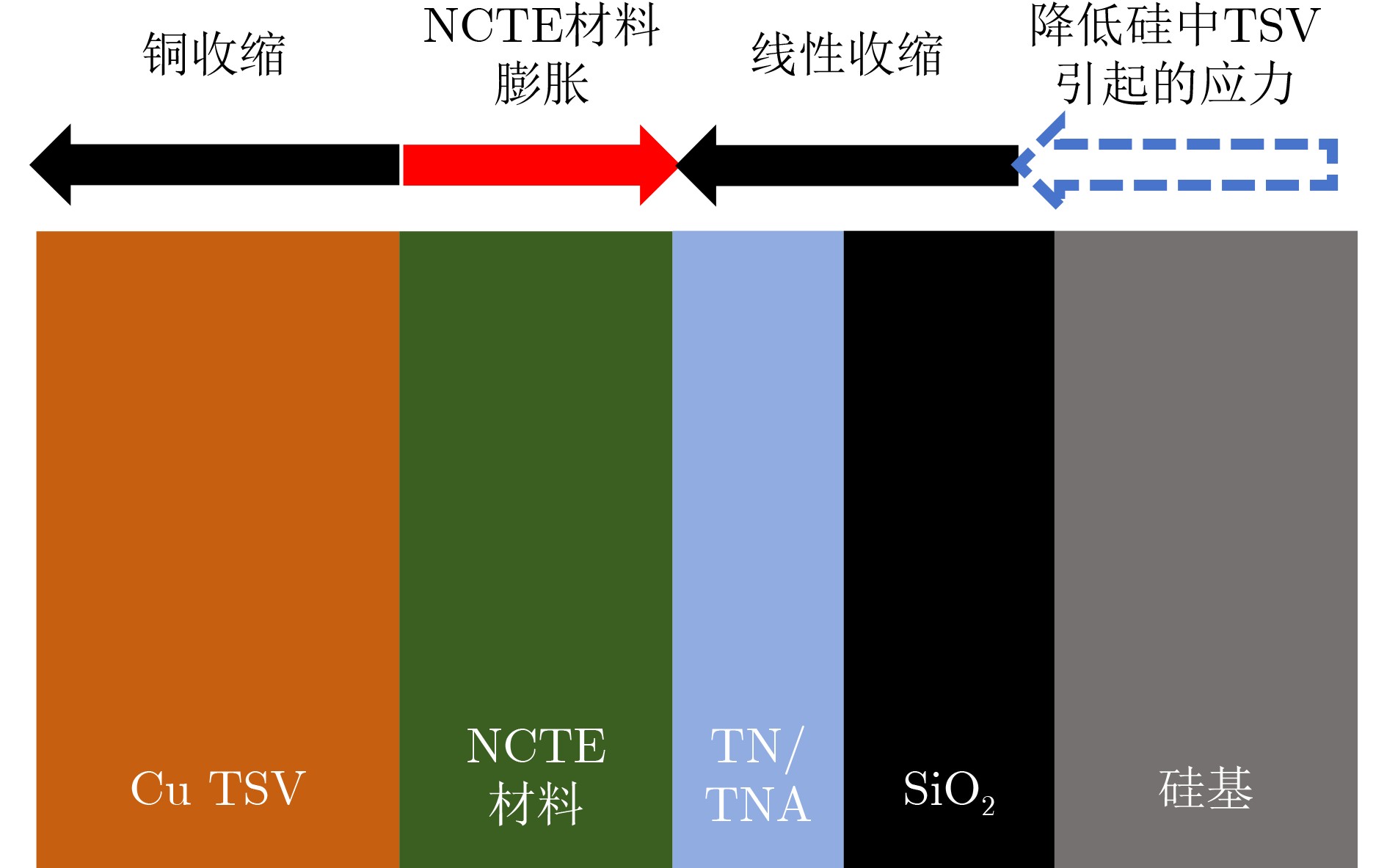
敏感的器件具有NCTE材料的TSV结构 [34] 具有高效应力补偿,减小禁布区,
提高芯片集成密度,不影响导热性能电阻率较高,仅在特定温度范围内有效,且材料制备困难,成本较高 高频通信与射频器件、
高密度存储器TTSV与微流冷却
混合散热[35]
[36]TSV改善纵向导热,微通道强化
横向散热,实现高效散热增加功耗和复杂度,制造成本高,具有流体泄漏风险 高性能计算芯片、
功耗分布不均的芯片 下载: 导出CSV
表 2 功耗控制与电源完整性硬件解决方案
方案名称 参考文献 主要优势 主要劣势 适用场景 分布式PDNTSV 布局 [13] 可显著降低供电路径阻抗,减少电源压降,延长器件寿命并提升能效 Bank平面面积增加约30%,布线
与时序收敛复杂度提高高带宽 3D-DRAM、HMC 基于网格结构的 RDL 设计 [37] 网格结构RDL可提升电流承载能力,在TSV数量相同条件下降低IR-drop 需新增网格金属,工艺成本和
布线阻塞增加TSV数量受限或分布不均的高电流异构3D-SoC/2.5D 封装 主动去耦 +FIVR 分层稳压 [38] 抑制71.1%衬底与 TSV 耦合引起的电源噪声且功耗开销仅1.11% 片上面积占用大;设计复杂 多层异构 TSV3D-IC和其他高电流、多电压域的 3DSoC 埋置式电源轨-BPDN [39] 降低IR-drop,释放前端布线资源,改善功率密度 需背面深刻蚀与绝缘处理,
热-机械失配待优化高并行移动SoC、AINPU 背供过孔-BPDN [40] 去掉顶层粗电源金属,缩短供电路径,兼顾工艺微缩与性能 晶圆减薄与密集nTSV良率挑战大,背面测试链尚不成熟 高性能CPU/GPU、数据中心
加速器直接背面接触 [41] 供电阻抗较另两种背面供电方案最小,抑制IR-drop与瞬态噪声,潜在性能最佳 需求极薄硅片与亚纳米级对准,
工艺窗口窄,仅实验验证超高频数字IP
下载: 导出CSV
-
[1] BOHR M. A 30 year retrospective on Dennard's MOSFET scaling paper[J]. IEEE Solid-State Circuits Society Newsletter, 2007, 12(1): 11–13. doi: 10.1109/N-SSC.2007.4785534. [2] ZHANG Shuye, LI Zhenfeng, ZHOU Hongzhi, et al. Challenges and recent prospectives of 3D heterogeneous integration[J]. e-Prime-Advances in Electrical Engineering, Electronics and Energy, 2022, 2: 100052. doi: 10.1016/j.prime.2022.100052. [3] CHEN Zhiwen, ZHANG Jiaju, WANG Shizhao, et al. Challenges and prospects for advanced packaging[J]. Fundamental Research, 2024, 4(6): 1455–1458. doi: 10.1016/j.fmre.2023.04.014. [4] LAU J H. Evolution, challenge, and outlook of TSV, 3D IC integration and 3D silicon integration[C]. The 2011 International Symposium on Advanced Packaging Materials (APM), Xiamen, China, 2011: 462–488. doi: 10.1109/ISAPM.2011.6105753. [5] VARTANIAN V, SMITH L, HUMMLER K, et al. Cost analysis of TSV process and scaling options[J]. International Symposium on Microelectronics, 2014, 2014(1): 1–7. doi: 10.4071/isom-TA11. [6] KIM D H and LIM S K. Impact of through-silicon-via scaling on the wirelength distribution of current and future 3D ICs[C]. Proceedings of the 2011 IEEE International Interconnect Technology Conference, Dresden, Germany, 2011: 1–3. doi: 10.1109/IITC.2011.5940324. [7] 郑俊平. 三维集成电路(3D IC)中硅通孔(TSV)链路的多场分析[D]. [博士论文], 西安电子科技大学, 2018.ZHENG Junping. Multi-field analysis of Through-Silicon Via (TSV) links in 3D ICs[D]. [Ph. D. dissertation], Xidian University, 2018. [8] SMITH M G and EMANUEL S. Methods of making thru-connections in semiconductor wafers[P]. US, 3343256A, 1967. [9] KONDO K, KADA M, and TAKAHASHI K. Three-Dimensional Integration of Semiconductors: Processing, Materials, and Applications[M]. Cham: Springer, 2015. doi: 10.1007/978-3-319-18675-7. [10] WANG Xiaodong, VASUDEVAN D, and LEE H H S. Global built-in self-repair for 3D memories with redundancy sharing and parallel testing[C]. 2011 IEEE International 3D Systems Integration Conference (3DIC), Osaka, Japan, 2012: 1–8. doi: 10.1109/3DIC.2012.6262967. [11] JEDEC. JEDEC Standard JESD235 High bandwidth memory (HBM) DRAM[S]. Arlington County: JEDEC Solid State Technology Association, 2013. [12] CHEN Dongdong, WANG Xianglong, YANG Yintang, et al. Intelligent codesign strategy for thermal management and cost control of 3-D integrated system with TTSV[J]. IEEE Transactions on Electron Devices, 2023, 70(10): 5265–5272. doi: 10.1109/TED.2023.3302825. [13] BOSE B and THAKKAR I. Characterization and mitigation of electromigration effects in TSV-based power delivery network enabled 3D-stacked DRAMs[C]. Proceedings of the 2021 Great Lakes Symposium on VLSI, USA, 2021: 101–107. doi: 10.1145/3453688.3461503. [14] HARB S M S and EISENSTADT W R. Impact of crosstalk on signal integrity of TSVs in 3D integrated circuits[J]. Advances Science, Technology and Engineering Systems Journal, 2018, 3(1): 109–114. doi: 10.25046/aj030113. [15] CUESTA D, RISCO-MARTÍN J L, AYALA J L, et al. Thermal-aware floorplanner for 3D IC, including TSVs, liquid microchannels and thermal domains optimization[J]. Applied Soft Computing, 2015, 34: 164–177. doi: 10.1016/j.asoc.2015.04.052. [16] ZHU Tianxiang, WANG Qipan, LIN Yibo, et al. MORE-Stress: Model order reduction based efficient numerical algorithm for thermal stress simulation of TSV arrays in 2.5D/3D IC[C]. 2025 Design, Automation & Test in Europe Conference (DATE), Lyon, France, 2025: 1–7. doi: 10.23919/DATE64628.2025.10993234. [17] XIA Qianfu, ZHANG Xinrui, MA Binghe, et al. A state-of-the-art review of through-silicon vias: Filling materials, filling processes, performance, and integration[J]. Advanced Engineering Materials, 2025, 27(1): 2401799. doi: 10.1002/adem.202401799. [18] PATHAK M, PAK J, PAN D Z, et al. Electromigration modeling and full-chip reliability analysis for BEOL interconnect in TSV-based 3D ICs[C]. 2011 IEEE/ACM International Conference on Computer-Aided Design (ICCAD), San Jose, USA, 2011: 555–562. doi: 10.1109/ICCAD.2011.6105385. [19] KIM J, CHEKURI V C K, RAHMAN N M, et al. Chiplet/Interposer co-design for power delivery network optimization in heterogeneous 2.5-D ICs[J]. IEEE Transactions on Components, Packaging and Manufacturing Technology, 2021, 11(12): 2148–2157. doi: 10.1109/TCPMT.2021.3113664. [20] 曹明鹏, 吴晓鹏, 管宏山, 等. 基于对偶单元法的三维集成微系统电热耦合分析[J]. 物理学报, 2021, 70(7): 074401. doi: 10.7498/aps.70.20201628.CAO Mingpeng, WU Xiaopeng, GUAN Hongshan, et al. Electrothermal coupling analysis of three-dimensional integrated microsystem based on dual cell method[J]. Acta Physica Sinica, 2021, 70(7): 074401. doi: 10.7498/aps.70.20201628. [21] JIAO Binbin, QIAO Jingping, JIA Shiqi, et al. Low stress TSV arrays for high-density interconnection[J]. Engineering, 2024, 38: 201–208. doi: 10.1016/j.eng.2023.11.023. [22] SRIDHAR A, VINCENZI A, RUGGIERO M, et al. 3D-ICE: Fast compact transient thermal modeling for 3D ICs with inter-tier liquid cooling[C]. 2010 IEEE/ACM International Conference on Computer-Aided Design (ICCAD), San Jose, USA, 2010: 463–470. doi: 10.1109/ICCAD.2010.5653749. [23] 罗山焱, 徐学良, 雷生吉, 等. 3D IC的热特性分析及预测[J]. 微电子学, 2024, 54(4): 665–670. doi: 10.13911/j.cnki.1004-3365.240118.LUO Shanyan, XU Xueliang, LEI Shengji, et al. Thermal characteristics analysis and estimation in 3D ICs[J]. Microelectronics, 2024, 54(4): 665–670. doi: 10.13911/j.cnki.1004-3365.240118. [24] OUKAIRA A, OUMLAZ M, ZBITOU J, et al. Integrated thermal management strategies for 3D chip stacking with through-silicon vias (TSV)[C]. The 4th International Conference on Innovative Research in Applied Science, Engineering and Technology (IRASET), FEZ, Morocco, 2024: 1–4. doi: 10.1109/IRASET60544.2024.10548169. [25] LIU Ziyue, LI Yixing, HU Jing, et al. DeepOHeat: Operator learning-based ultra-fast thermal simulation in 3D-IC design[C]. The 60th ACM/IEEE Design Automation Conference (DAC), San Francisco, USA, 2023: 1–6. doi: 10.1109/DAC56929.2023.10247998. [26] KUMAR A, CHANG N, GEB D, et al. ML-based fast on-chip transient thermal simulation for heterogeneous 2.5D/3D IC designs[C]. 2022 International Symposium on VLSI Design, Automation and Test (VLSI-DAT), Hsinchu, China, 2022: 1–8. doi: 10.1109/VLSI-DAT54769.2022.9768082. [27] KANDLIKAR S G and GANGULY A. Fundamentals of heat dissipation in 3D IC packaging and thermal-aware design[M]. LI Yan and GOYAL D. 3D Microelectronic Packaging: From Architectures to Applications. 2nd ed. Singapore: Springer, 2021: 369–395. doi: 10.1007/978-981-15-7090-2_13. [28] WANG Fengjuan, LI Yue, YU Ningmei, et al. Effectiveness of thermal redistribution layer in cooling of 3D ICs[J]. International Journal of Numerical Modelling: Electronic Networks, Devices and Fields, 2021, 34(3): e2847. doi: 10.1002/jnm.2847. [29] XU Peng, HUANG Huan, ZHANG Bingqi, et al. Thermal performance analysis of carbon materials based TSV in three dimensional integrated circuits[J]. IEEE Access, 2023, 11: 75285–75294. doi: 10.1109/ACCESS.2023.3297222. [30] WANG Xianglong, YANG Yintang, CHEN Dongdong, et al. A high-efficiency design method of TSV array for thermal management of 3-D integrated system[J]. IEEE Transactions on Computer-Aided Design of Integrated Circuits and Systems, 2023, 42(6): 1733–1741. doi: 10.1109/TCAD.2022.3213610. [31] LIANG Jingyang, NING Minjie, DING Chao, et al. The effect of silicon anisotropy on the thermal stress of TSV structure of 3D packaging chip under thermal cyclic loads[C]. The 22nd International Conference on Electronic Packaging Technology (ICEPT), Xiamen, China, 2021: 1–4. doi: 10.1109/ICEPT52650.2021.9567933. [32] LIAO Shuaidong, HUANG Chunyue, ZHANG Huaiquan, et al. Thermal stress study of 3D IC based on TSV and verification of thermal dissipation of STI[C]. 2021 22nd International Conference on Electronic Packaging Technology (ICEPT), Xiamen, China, 2021: 1–5. doi: 10.1109/ICEPT52650.2021.9568038. [33] SAZALI S B, HASSAN H B, YUSOF N, et al. Optimization of design parameters using Taguchi method for thermal stress analysis in a 3D IC[C]. 2024 IEEE 14th Symposium on Computer Applications & Industrial Electronics (ISCAIE), Penang, Malaysia, 2024: 1–4. doi: 10.1109/ISCAIE61308.2024.10576559. [34] KINO H, FUKUSHIMA T, and TANAKA T. Suppression of TSV-induced stress by using negative thermal expansion material[C]. 2024 International 3D Systems Integration Conference (3DIC), Sendai, Japan, 2024: 1–3. doi: 10.1109/3DIC63395.2024.10830164. [35] SHI Bing, SRIVASTAVA A, and BAR-COHEN A. Co-design of micro-fluidic heat sink and thermal through-silicon-vias for cooling of three-dimensional integrated circuit[J]. IET Circuits, Devices & Systems, 2013, 7(5): 223–231. doi: 10.1049/iet-cds.2013.0026. [36] WANG Kangjia, SUN Hongchang, and WANG Kuizhi. A micro-channel cooling model for a three-dimensional integrated circuit considering through-silicon vias[J]. Micro and Nanosystems, 2021, 13(1): 49–54. doi: 10.2174/1876402912666200123154001. [37] XU Kan and FRIEDMAN E G. Grid-based redistribution layers within 3-D power networks[J]. IEEE Transactions on Components, Packaging and Manufacturing Technology, 2021, 11(4): 672–682. doi: 10.1109/TCPMT.2021.3068350. [38] HUANG P T, TSAI T H, YANG P J, et al. Hierarchical active voltage regulation for heterogeneous TSV 3D-ICs[C]. 2020 IEEE 33rd International System-on-Chip Conference (SOCC), Las Vegas, USA, 2020: 242–247. doi: 10.1109/SOCC49529.2020.9524797. [39] PRASAD D, NIBHANUPUDI S S T, DAS S, et al. Buried power rails and back-side power grids: Arm® CPU power delivery network design beyond 5nm[C]. 2019 IEEE International Electron Devices Meeting (IEDM), San Francisco, USA, 2019: 19.1. 1–19.1. 4. doi: 10.1109/IEDM19573.2019.8993617. [40] HAFEZ W, AGNIHOTRI P, ASORO M, et al. Intel PowerVia technology: Backside power delivery for high density and high-performance computing[C]. 2023 IEEE Symposium on VLSI Technology and Circuits (VLSI Technology and Circuits), Kyoto, Japan, 2023: 1–2. doi: 10.23919/VLSITechnologyandCir57934.2023.10185208. [41] RADOSAVLJEVIć M, HUANG C Y, GALATAGE R, et al. Demonstration of a stacked CMOS inverter at 60nm gate pitch with power via and direct backside device contacts[C]. 2023 International Electron Devices Meeting (IEDM), San Francisco, USA, 2023: 1–4. doi: 10.1109/IEDM45741.2023.10413678. [42] ZHU Lingjun, JO C, and LIM S K. Power delivery solutions and PPA impacts in micro-bump and hybrid-bonding 3D ICs[J]. IEEE Transactions on Components, Packaging and Manufacturing Technology, 2022, 12(12): 1969–1982. doi: 10.1109/TCPMT.2022.3221025. [43] HAJ-YAHYA J, ALSER M, KIM J, et al. SysScale: Exploiting multi-domain dynamic voltage and frequency scaling for energy efficient mobile processors[C]. 2020 ACM/IEEE 47th Annual International Symposium on Computer Architecture (ISCA), Valencia, Spain, 2020: 227–240. doi: 10.1109/ISCA45697.2020.00029. [44] MAIOLI A, QUINONES K A, AHMED S, et al. Dynamic voltage and frequency scaling for intermittent computing[J]. ACM Transactions on Sensor Networks, 2025, 21(2): 16. doi: 10.1145/3714470. [45] KIM H, LEE S, PARK D, et al. Power integrity design of mobile 3D-IC based on the allocation of optimal number of TSV, BGA, and via[C]. 2023 IEEE Electrical Design of Advanced Packaging and Systems (EDAPS), Rose-Hill, Mauritius, 2023: 1–3. doi: 10.1109/EDAPS58880.2023.10468263. [46] LIU Ziyu, JIANG Han, ZHU Ziyuan, et al. Crosstalk noise of octagonal TSV array arrangement based on different input signal[J]. Processes, 2022, 10(2): 260. doi: 10.3390/pr10020260. [47] CHO K, KIM Y, LEE H, et al. Signal integrity design and analysis of differential high-speed serial links in silicon interposer with through-silicon via[J]. IEEE Transactions on Components, Packaging and Manufacturing Technology, 2019, 9(1): 107–121. doi: 10.1109/TCPMT.2018.2843442. [48] LIU Ziyu, JIANG Han, ZHU Zhiyuan, et al. Thermal-mechanical and signal reliability of a new differentiated TSV[J]. IEEE Transactions on Electron Devices, 2022, 69(10): 5766–5772. doi: 10.1109/TED.2022.3199332. [49] ZHAO Zhibo, LI Jinkai, YUAN Haoyun, et al. Electrical characterization of through-silicon-via-based coaxial line for high-frequency 3D integration (Invited Paper)[J]. Electronics, 2022, 11(20): 3417. doi: 10.3390/electronics11203417. [50] ARAGA Y, WATANABE N, SHIMAMOTO H, et al. Analysis and evaluation of noise coupling between through-silicon-vias[J]. IEICE Electronics Express, 2021, 18(11): 20210139. doi: 10.1587/elex.18.20210139. [51] CHANDRAKAR M and MAJUMDER M K. Impact of polymer liners on crosstalk induced delay of different TSV shapes[J]. IETE Journal of Research, 2024, 70(1): 686–699. doi: 10.1080/03772063.2022.2108915. [52] TIAN Miao and GU Xiaokun. Alternative insulation liners for through-silicon vias: A comprehensive review[J]. Materials Science in Semiconductor Processing, 2023, 166: 107726. doi: 10.1016/j.mssp.2023.107726. [53] OH S, ZHENG Ting, and BAKIR M S. Electrical characterization of shielded TSVs with airgap isolation for RF/mmWave applications[J]. IEEE Transactions on Components, Packaging and Manufacturing Technology, 2024, 14(2): 202–210. doi: 10.1109/TCPMT.2024.3358102. [54] KIM H, PARK J, LEE S, et al. Signal integrity analysis of through-silicon-via (TSV) with passive equalizer to separate return path and mitigate the inter-symbol interference (ISI) for next generation high bandwidth memory[J]. IEEE Transactions on Components, Packaging and Manufacturing Technology, 2023, 13(12): 1973–1988. doi: 10.1109/TCPMT.2023.3334789. [55] CHANDRAKAR S, GUPTA D, and MAJUMDER M K. Impact of TSV bump and redistribution layer on crosstalk delay and power loss[J]. Memories-Materials, Devices, Circuits and Systems, 2023, 4: 100040. doi: 10.1016/j.memori.2023.100040. [56] TSAI Y C, LEE C H, CHANG H C, et al. Electrical characteristics and reliability of wafer-on-wafer (WOW) bumpless through-silicon via[J]. IEEE Transactions on Electron Devices, 2021, 68(7): 3520–3525. doi: 10.1109/TED.2021.3082497. [57] OHBA T, SAKUI K, SUGATANI S, et al. Review of bumpless build cube (BBCube) using wafer-on-wafer (WOW) and chip-on-wafer (COW) for tera-scale three-dimensional integration (3DI)[J]. Electronics, 2022, 11(2): 236. doi: 10.3390/electronics11020236. [58] CHEW S A, DE VOS J, and BEYNE E. Wafer-to-wafer hybrid bonding at 400-nm interconnect pitch[J]. Nature Reviews Electrical Engineering, 2024, 1(2): 71–72. doi: 10.1038/s44287-024-00019-8. [59] CHOI K S, JOO J, CHOI G M, et al. Chip-on-wafer (CoW) technology utilizing laser-assisted bonding with compression (LABC) for bump counts exceeding 500, 000 at a 20 µm pitch[C]. 2024 IEEE 74th Electronic Components and Technology Conference (ECTC), Denver, USA, 2024: 943–948. doi: 10.1109/ECTC51529.2024.00153. -

 下载:
下载:


图(7) / 表(2)
计量
- 文章访问数: 2948
- HTML全文浏览量: 1956
- PDF下载量: 407
- 被引次数: 0
