

Low Switching Loss Double Trench SiC MOSFET with Integrated JFET Continuity Diode
-
摘要: 传统双沟槽碳化硅金属氧化物半导体场效应晶体管(SiC MOSFET)在高频开关电路和反向续流应用中显现出显著的性能瓶颈,主要表现为开关损耗较高、反向导通电压偏大、反向恢复电荷过多,以及长时间反向续流易引发双极退化等问题。为突破这些技术限制,该文采用TCAD仿真技术,基于PN结空间电荷区内能带弯曲的物理机制,设计一种集成结型场效应晶体管(JFET)的双沟槽SiC MOSFET (IJ-MOS)。与传统SiC MOSFET (CON-MOS)相比,IJ-MOS在性能上取得了显著提升:其反向导通电压从CON-MOS的2.92 V降至1.83 V,反向恢复电荷减少43.7%,反向恢复峰值电流下降31.7%,总开关损耗削减24.2%。此外,IJ-MOS通过有效抑制反向续流时体二极管的激活,显著降低了双极退化的发生概率,从而增强了器件的长期可靠性。这一新型设计使IJ-MOS成为高频开关电路和反向续流应用中更为优越的解决方案。
-
关键词:
- SiC MOSFET /
- 双极退化 /
- 反向导通 /
- 开关损耗
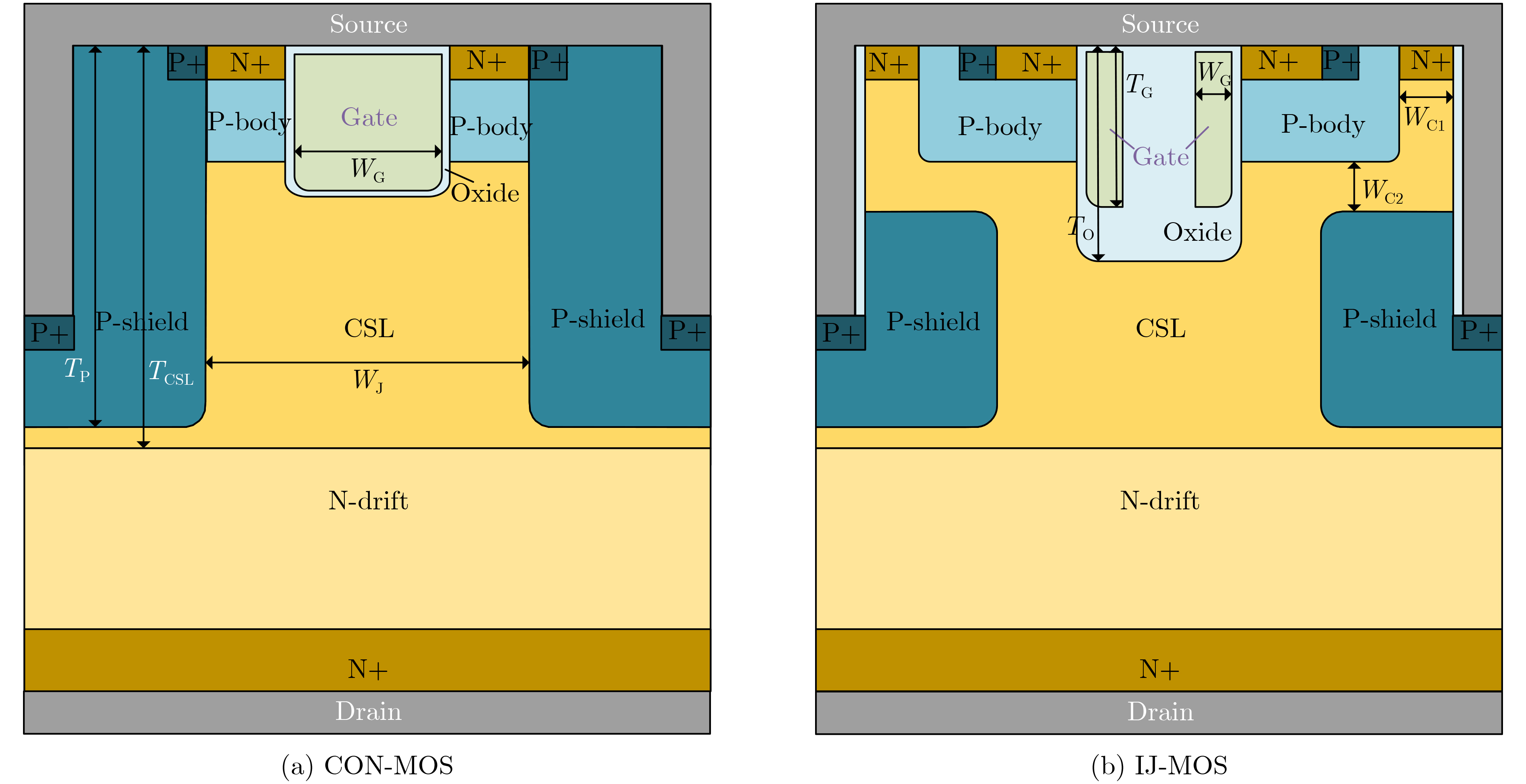
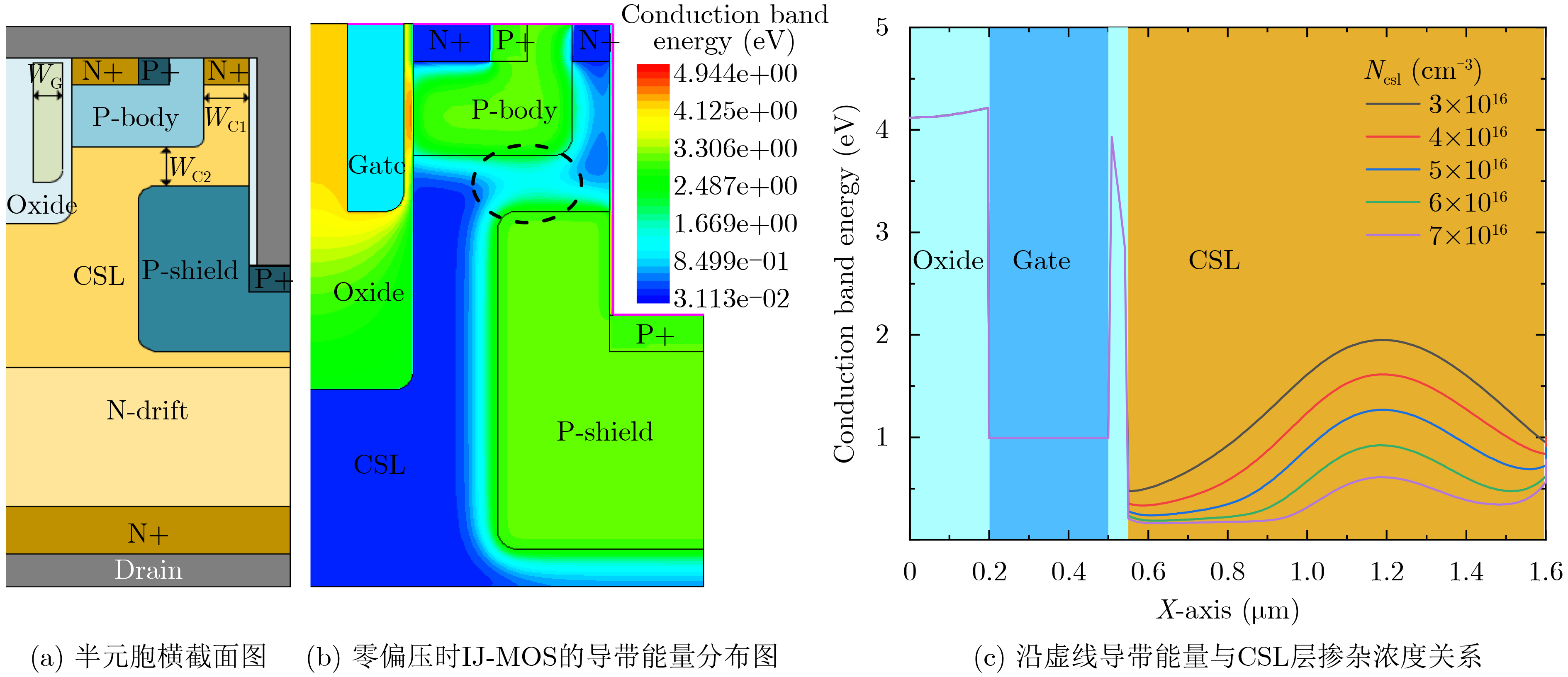
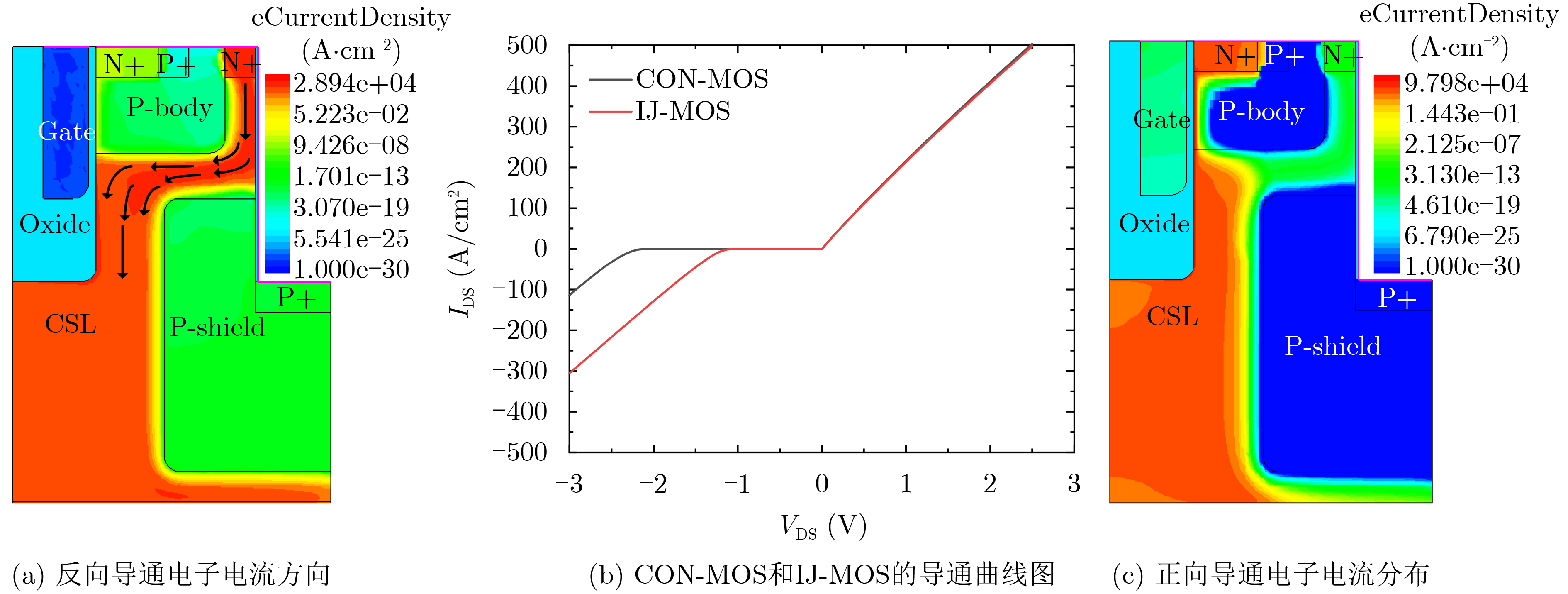
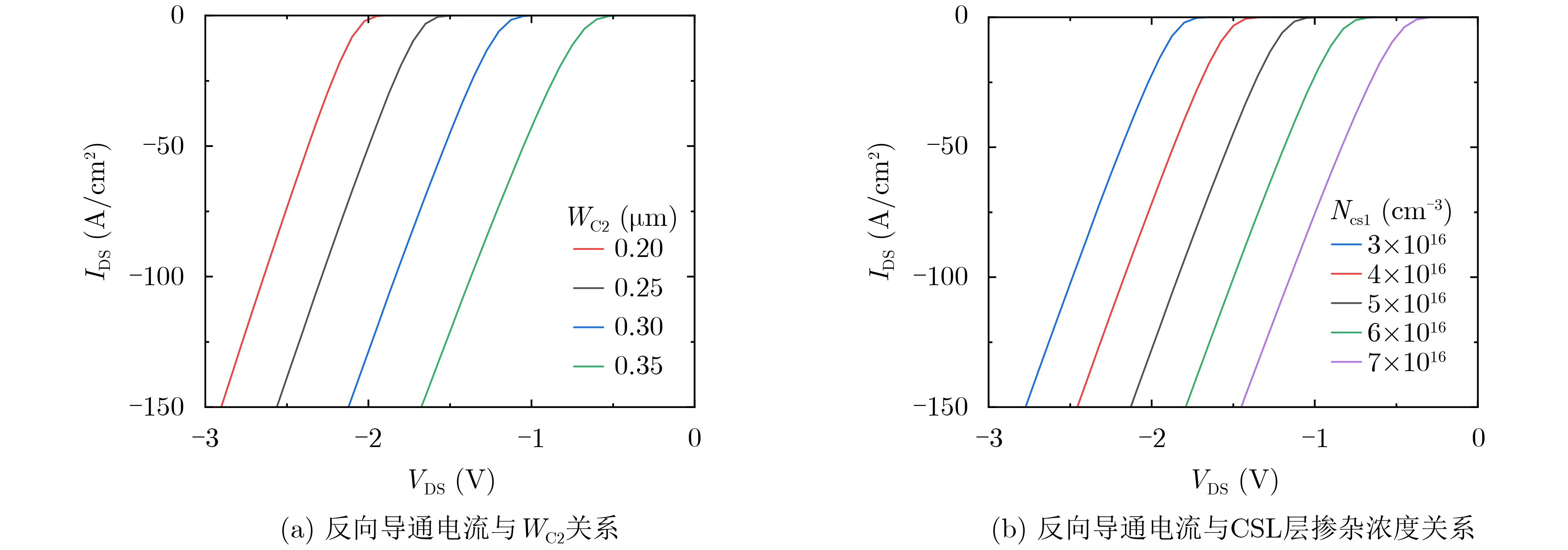
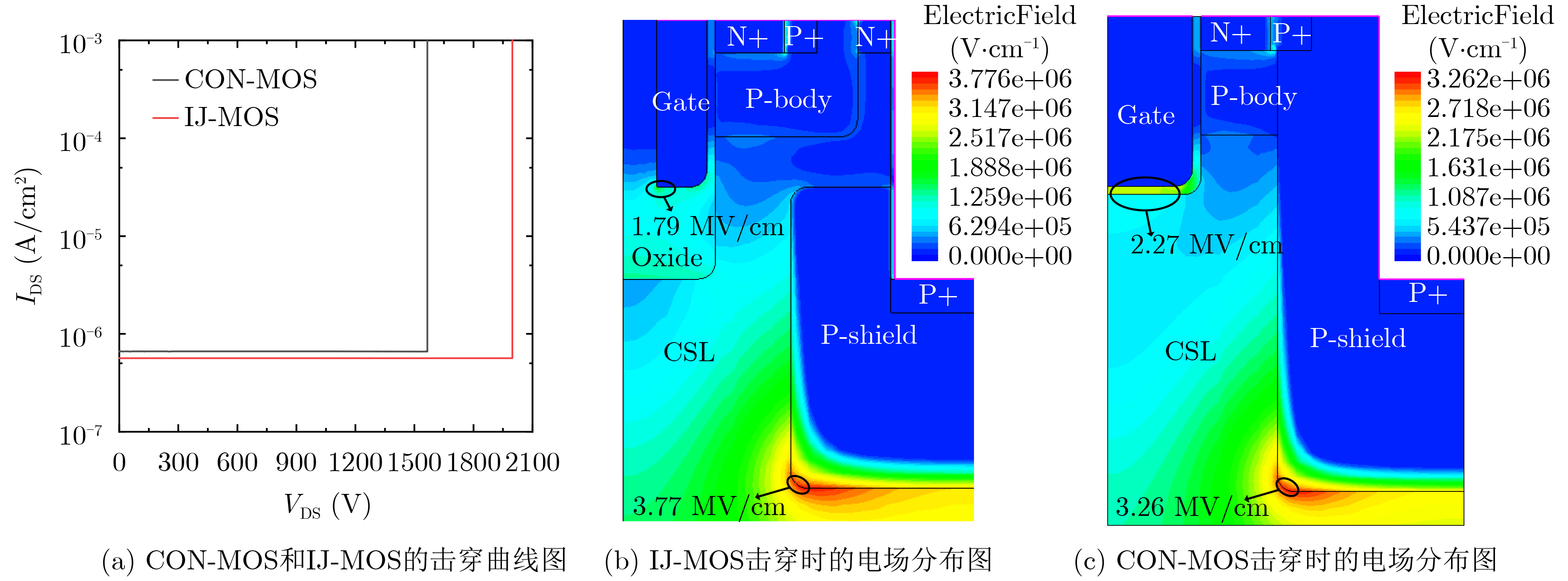
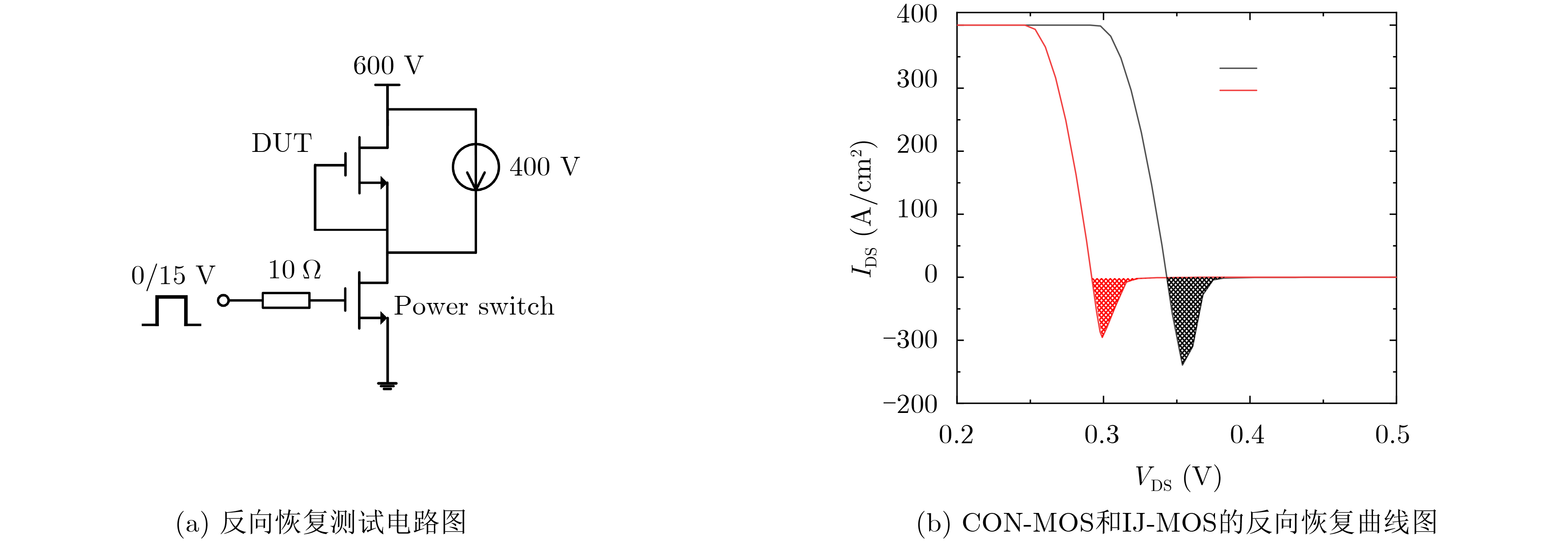
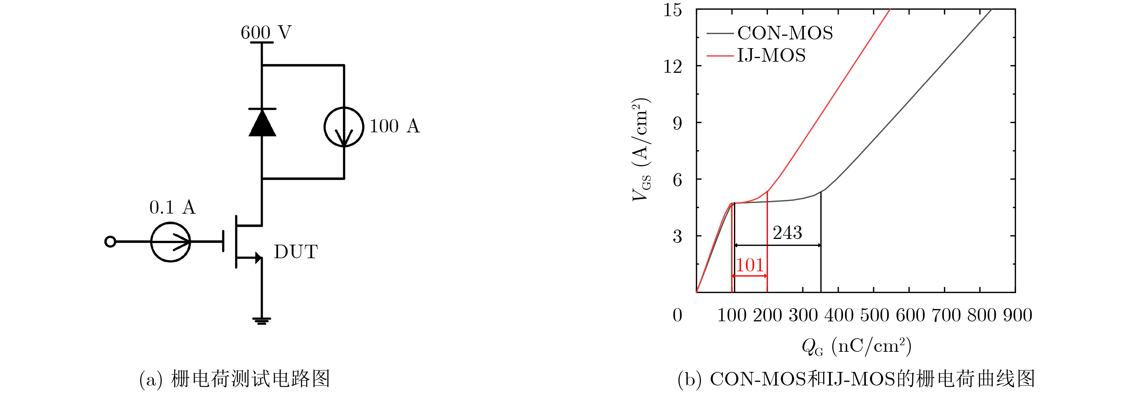
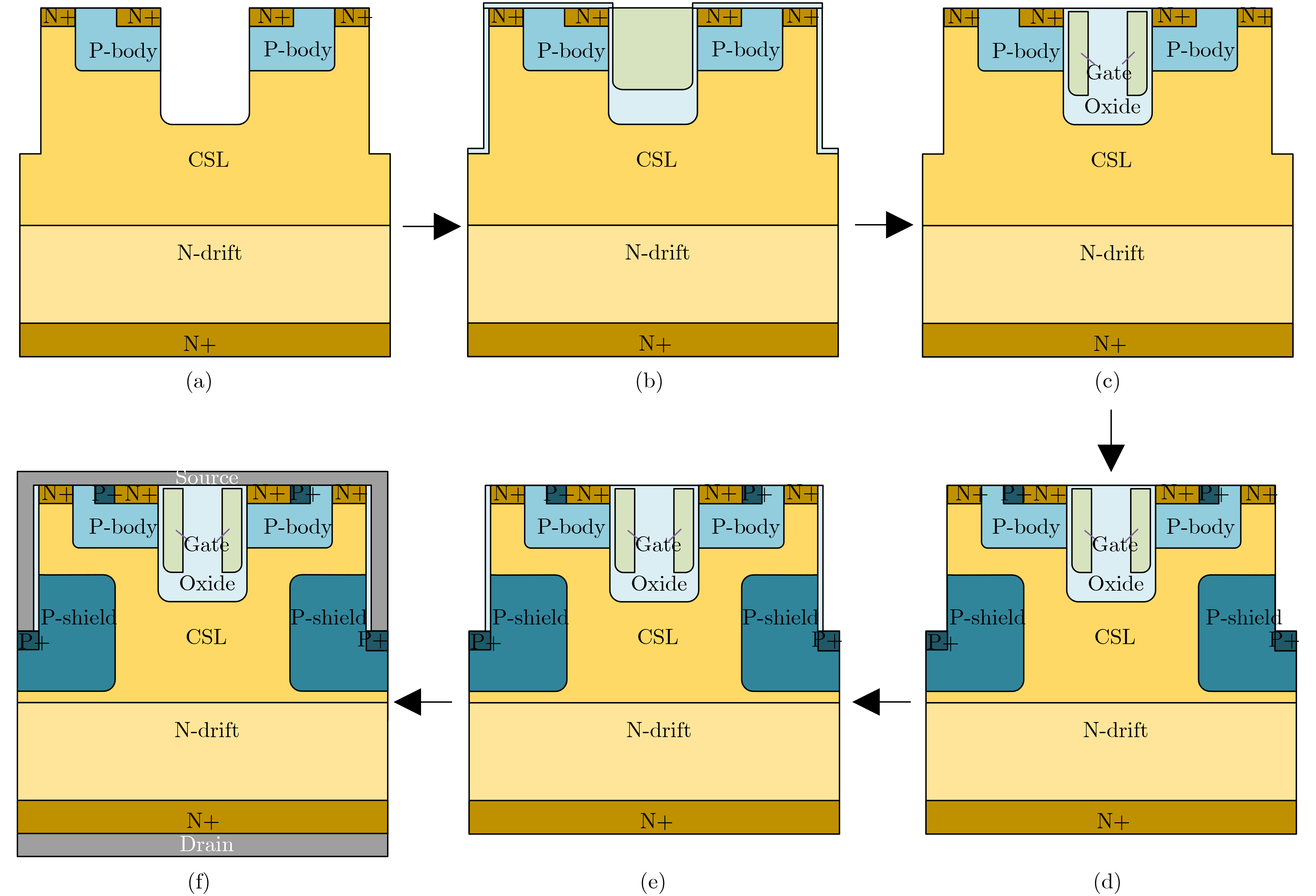
Abstract:Objective Silicon Carbide Metal Oxide Semiconductor Field Effect Transistors (SiC MOSFETs) are considered ideal power devices for power systems due to their ultra-low on-resistance and excellent switching characteristics. However, Conventional SiC MOSFETs (CON-MOS) present considerable limitations in reverse current applications. These limitations stem primarily from their reliance on the body diode during reverse conduction, which exhibits a high reverse conduction voltage, significant reverse recovery loss, and is prone to bipolar degradation during long-term operation, adversely affecting power system stability. Furthermore, CON-MOS devices in high-frequency switching circuits suffer from substantial switching losses, reducing overall circuit efficiency. A widely adopted solution is to connect an external Schottky Barrier Diode (SBD) in parallel to enhance reverse current continuity. However, this approach increases device size and parasitic capacitance. Moreover, Schottky contacts are susceptible to large reverse leakage currents at elevated temperatures. Although SiC MOSFETs with integrated SBDs mitigate issues caused by external parallel SBDs, they still exhibit degraded blocking characteristics and thermal stability. SiC MOSFETs incorporating integrated MOS channel diodes have also been proposed to improve reverse conduction performance. Nonetheless, these devices raise reliability concerns due to increased process complexity and the presence of an ultra-thin (10 nm) oxide layer. Alternative industry structures employing polysilicon heterojunctions with 4H-SiC epitaxial layers aim to enhance reverse current continuity in SiC MOSFETs. However, these structures exhibit high reverse leakage currents and lack avalanche capability, primarily because the heterojunction barrier is insufficient to sustain the full blocking voltage. Devices integrating channel accumulation diodes have demonstrated lower reverse conduction voltage and reduced reverse recovery charge. Nevertheless, the barrier height in these designs is highly sensitive to oxide layer thickness, imposing stricter process control requirements. To address these challenges, this paper proposes an Integrated Junction Field Effect Transistor (JFET) SiC MOSFET (IJ-MOS) structure. The IJ-MOS effectively reduces reverse recovery loss, eliminates bipolar degradation, and significantly improves performance and reliability in reverse continuous current applications. Methods Technology Computer-Aided Design (TCAD) simulations are conducted to evaluate the performance of the proposed and conventional structures. Several critical models are included in the simulation process, such as mobility saturation under high electric fields, Auger recombination, Okuto-Crowell impact ionization, bandgap narrowing, and incomplete ionization. Furthermore, the effects of traps and fixed charges at the SiC/SiO2 interface are also considered. This study proposes an IJ-MOS structure based on the physical mechanism of energy band bending within the space charge region of the PN junction. Specifically, the IJ-MOS blocks the intermediate channel region through PN junctions formed between the Current Spreading Layer (CSL) and the P-body and P-shield layers, respectively. The blocking mechanism relies on the PN junction inducing conduction band bending within the CSL layer, thereby raising the conduction band energy and forming a barrier region. During reverse conduction, the integrated JFET provides a unipolar, low-barrier reverse conduction path, which mitigates bipolar degradation and significantly reduces reverse recovery charge. This improves device performance and reliability under reverse current conditions. Furthermore, the IJ-MOS reduces gate-drain coupling by separating the polysilicon gate and extended oxide structure, while optimising the internal electric field distribution. These design features enhance the device’s blocking voltage capability, increasing the potential of IJ-MOS for high-voltage applications. Results and Discussions Simulation results indicate that, compared to CON-MOS, the proposed IJ-MOS structure significantly reduces the reverse conduction voltage from 2.92 V in CON-MOS to 1.83 V ( Fig. 3 ). The reverse recovery charge is reduced by 43.7%, and the peak reverse recovery current decreases by 31.7%, while maintaining comparable forward conduction characteristics (Fig. 7 ). Furthermore, due to the split gate and extended oxide structure, the IJ-MOS exhibits a lower gate-drain capacitance, effectively reducing the coupling between the gate and drain. The extended oxide layer also improves the internal electric field distribution, leading to an increase in breakdown voltage and a 60% improvement in the Baliga Figure of Merit (BFOM) (Table 2 ). Benefiting from the lower gate-drain capacitance, the total switching loss of IJ-MOS is reduced by 24.2% compared to CON-MOS (Fig. 8 ).Conclusions This paper proposes a novel SiC MOSFET structure evaluated through TCAD simulation. The proposed IJ-MOS reduces reverse conduction voltage and significantly lowers reverse recovery charge, thereby enhancing reverse conduction performance. Since the barrier region of the integrated JFET is lower than that of the PN junction, the JFET conducts prior to the body diode, which effectively suppresses bipolar conduction of the body diode and avoids bipolar degradation. The primary carriers in the JFET are electrons rather than both electrons and holes, meaning only electrons must be removed during the reverse recovery process, reducing reverse recovery charge. Additionally, the split gate and extended oxide structure reduce gate-drain coupling, which decreases gate-drain capacitance, switching time, and overall switching losses. These advantages make the IJ-MOS a promising candidate for high-performance power electronics applications. -
表 1 IJ-MOS和CON-MOS主要参数
器件参数 IJ-MOS CON-MOS 沟槽栅深度TG(μm) 1 1 栅宽WG(μm) 0.3 1 P-shield区厚度TP(μm) 2.8 2.8 栅氧化层深度TO(μm) 1.55 1.05 JFET区宽度WJ(μm) 2 2 沟道一区宽度WC1(μm) 0.2 - 沟道二区宽度WC2(μm) 0.3 - CSL层厚度TCSL(μm) 3 3 总外延层厚度(μm) 12 12 P-shield掺杂浓度(cm–3) 1×10¹⁸ 1×10¹⁸ P+掺杂浓度(cm–3) 1×10¹⁹ 1×10¹⁹ N+掺杂浓度(cm–3) 1×10¹⁹ 1×10¹⁹ P-body掺杂浓度(cm–3) 1×10¹⁷ 1×10¹⁷ CSL掺杂浓度(cm–3) 5×10¹⁶ 5×10¹⁶ N-drift掺杂浓度(cm–3) 3×10¹⁵ 3×10¹⁵ 元胞宽度WCELL(μm) 4.2 4.2  下载: 导出CSV
表 2 CON-MOS 和 IJ-MOS 的主要特性
器件特性 IJ-MOS CON-MOS VON(V) 1.83 2.92 BV(V) 1998 1566 Ron,sp(mΩ/cm2) 4.68 4.62 BFOM(BV2/Ron,sp) (MW/cm2) 0.85 0.53 IRRM(A/cm2) 95 139 QRR(μC/cm2) 1.29 2.29 QGD(nC/cm2) 101 243 EON(mJ/cm2) 1.07 1.34 EOFF(mJ/cm2) 2.05 2.78 ESW(mJ/cm2) 3.12 4.12
下载: 导出CSV
-
[1] JIANG Huaping, WEI Jin, DAI Xiaoping, et al. SiC MOSFET with built-in SBD for reduction of reverse recovery charge and switching loss in 10-kV applications[C]. Proceedings of 2017 29th International Symposium on Power Semiconductor Devices and IC’s (ISPSD), Sapporo, Japan, 2017: 49–52. doi: 10.23919/ISPSD.2017.7988890. [2] SUNG W and BALIGA B J. On developing one-chip integration of 1.2 kV SiC MOSFET and JBS diode (JBSFET)[J]. IEEE Transactions on Industrial Electronics, 2017, 64(10): 8206–8212. doi: 10.1109/TIE.2017.2696515. [3] LI Xuan, TONG Xing, HUANG A Q, et al. SiC trench MOSFET with integrated self-assembled three-level protection Schottky barrier diode[J]. IEEE Transactions on Electron Devices, 2018, 65(1): 347–351. doi: 10.1109/TED.2017.2767904. [4] LUO Maojiu, CHEN Hang, ZHANG Yourun, et al. Novel design and modelling of SiC junction barrier Schottky diode with improved Baliga FOM under high-temperature applications[J]. Microelectronics Journal, 2024, 151: 106343. doi: 10.1016/j.mejo.2024.106343. [5] OHOKA A, UCHIDA M, KIYOSAWA T, et al. Reduction of RonA retaining high threshold voltage in SiC DioMOS by improved channel design[C]. 2018 IEEE 30th International Symposium on Power Semiconductor Devices and ICs (ISPSD), Chicago, USA, 2018: 52–55. doi: 10.1109/ISPSD.2018.8393600. [6] UCHIDA M, HORIKAWA N, TANAKA K, et al. Novel SiC power MOSFET with integrated unipolar internal inverse MOS-channel diode[C]. 2011 International Electron Devices Meeting, Washington, USA, 2011: 26.6. 1–26.6. 4. doi: 10.1109/IEDM.2011.6131620. [7] OHOKA A, HORIKAWA N, KIYOSAWA T, et al. 40mΩ/1700V DioMOS (Diode in SiC MOSFET) for high power switching applications[J]. Materials Science Forum, 2014, 778/780: 911–914. doi: 10.4028/www.scientific.net/MSF.778-780.911. [8] NA J and KIM K. A novel 4H-SiC double trench MOSFET with built-in MOS channel diode for improved switching performance[J]. Electronics, 2023, 12(1): 92. doi: 10.3390/electronics12010092. [9] WEI Jie, JIANG Qingfeng, LUO Xiaorong, et al. High performance SiC trench-type MOSFET with an integrated MOS-channel diode[J]. Chinese Physics B, 2023, 32(2): 028503. doi: 10.1088/1674-1056/ac7cd5. [10] WU Lijuan, YANG Guanglin, YANG Deqiang, et al. Self-clamped P-shield 4H-SiC trench MOSFET for low turn-off loss and suppress switching oscillation[J]. Microelectronics Journal, 2024, 151: 106307. doi: 10.1016/j.mejo.2024.106307. [11] CHEN Hang, ZHANG Yourun, ZHOU Rong, et al. A novel low on-state resistance Si/4H-SiC heterojunction VDMOS with electron tunneling layer based on a discussion of the hetero-transfer mechanism[J]. Crystals, 2023, 13(5): 778. doi: 10.3390/cryst13050778. [12] JIANG Kaizhe, ZHANG Xiaodong, TIAN Chuan, et al. A SiC asymmetric cell trench MOSFET with a split gate and integrated p+-poly Si/SiC heterojunction freewheeling diode[J]. Chinese Physics B, 2023, 32(5): 058504. doi: 10.1088/1674-1056/acbd2d. [13] FU Hao, WEI Jiaxing, WEI Zhaoxiang, et al. Theory and design of novel power poly-Si/SiC heterojunction tunneling transistor structure[J]. IEEE Transactions on Electron Devices, 2023, 70(11): 6086–6092. doi: 10.1109/TED.2023.3317004. [14] WANG Qingyuan, WANG Ying, FEI Xinxing, et al. Performance enhancement of 1.7 kV MOSFET using PIN-junction gate and integrated heterojunction[J]. Microelectronics Reliability, 2024, 152: 115305. doi: 10.1016/j.microrel.2023.115305. [15] GAO Sheng, ZHANG Xianfeng, WANG Qi, et al. Asymmetric trench SiC MOSFET with integrated channel accumulation diode for enhanced reverse conduction and switching characteristics[J]. Microelectronics Journal, 2024, 153: 106436. doi: 10.1016/j.mejo.2024.106436. -

 下载:
下载:


图(10) / 表(2)
计量
- 文章访问数: 685
- HTML全文浏览量: 434
- PDF下载量: 49
- 被引次数: 0
