

A Novel Silicon Carbide (SiC) MOSFET with Schottky Diode Integration Technology
-
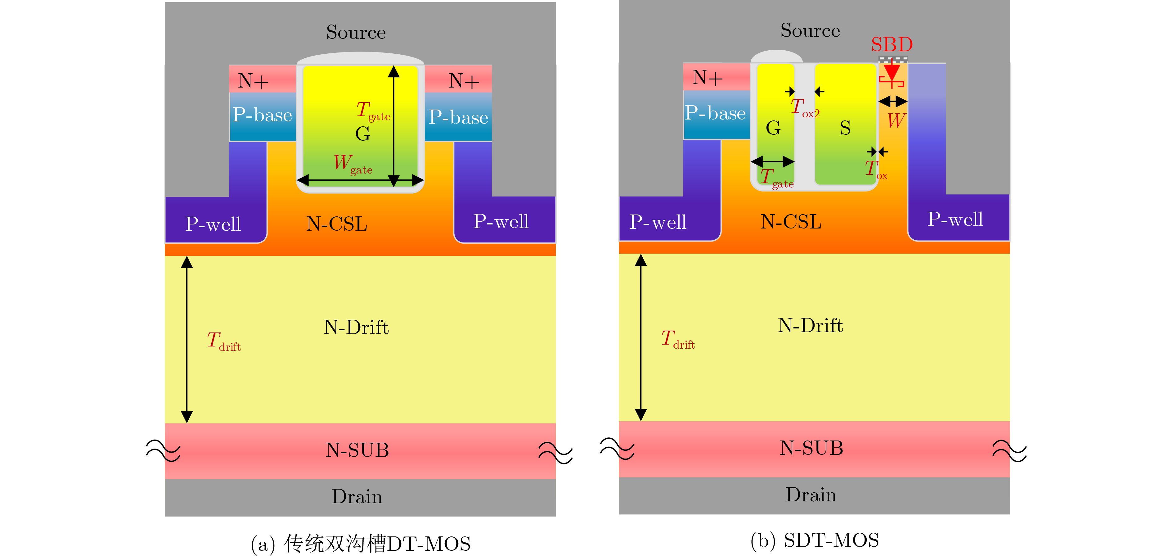
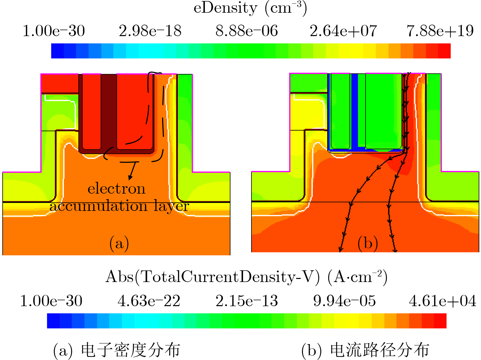
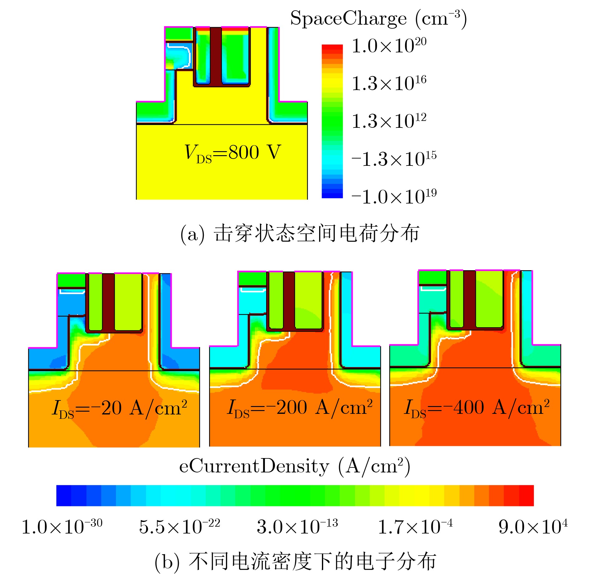
摘要: 该文提出一种集成肖特基二极管结构的新型分裂栅碳化硅MOSFET器件,有效改善传统DT-MOS器件的反向恢复与开关特性。该新型结构首先采用元胞内集成肖特基二极管技术替代传统DT-MOS的右侧沟道,其次采用分裂栅极集成技术代替传统槽栅设计,将栅极分成了栅极G和源极S两个部分,中间由二氧化硅进行介质隔离。其作用包括:集成肖特基二极管抑制体二极管导通并消除双极退化效应;集成分裂栅与源极短接,减小栅漏耦合面积来降低反馈电容与栅电荷,且在接入高电位时形成电子积累层以提高电子密度。其结果显示:反向导通状态下,电流将从肖特基二极管流出,连接源极的分裂栅极将提升电子浓度从而提高电流密度;动态开关状态下,分裂栅结构通过屏蔽设计减小了栅极与漏极的耦合面积,有效降低了米勒平台电荷QGD并改善了开关性能。
-
关键词:
- 肖特基二极管 /
- 碳化硅 MOSFET双极退化效应 /
- 分裂栅极
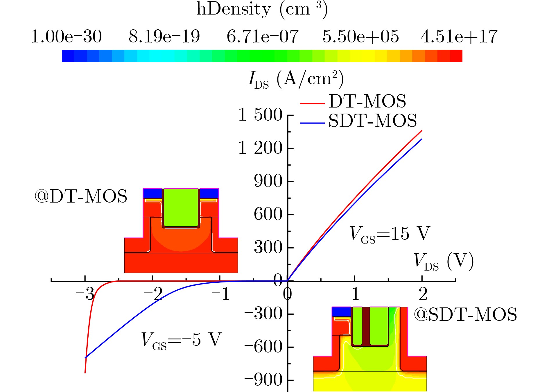
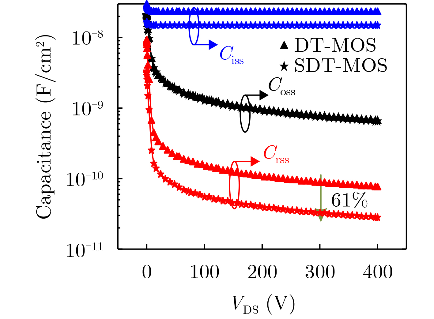
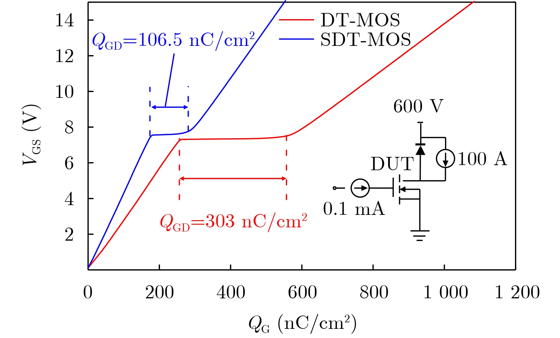
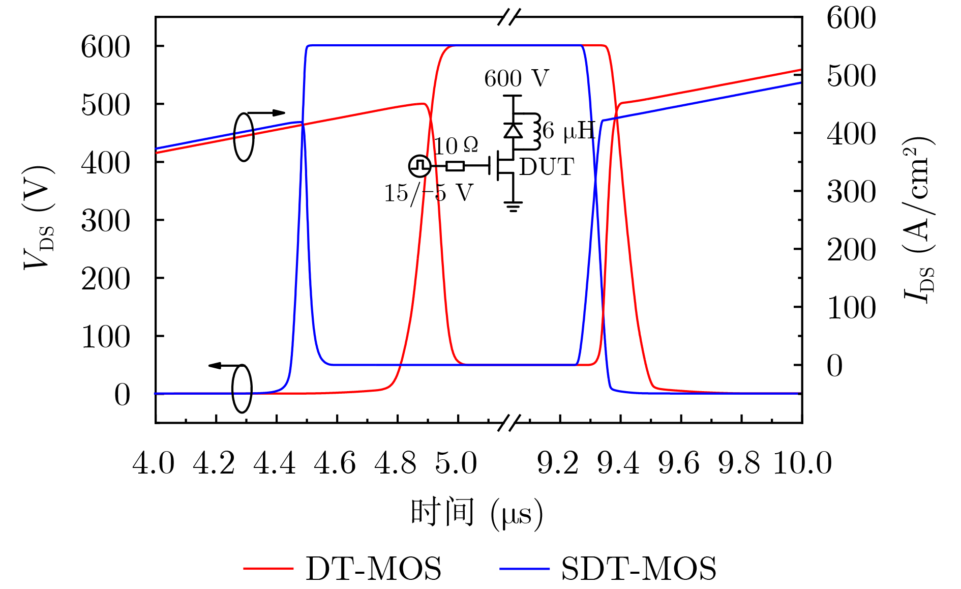
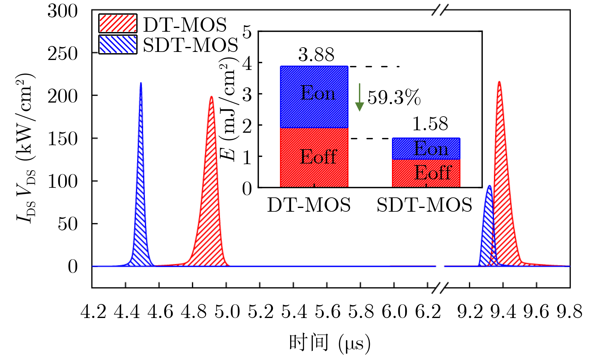
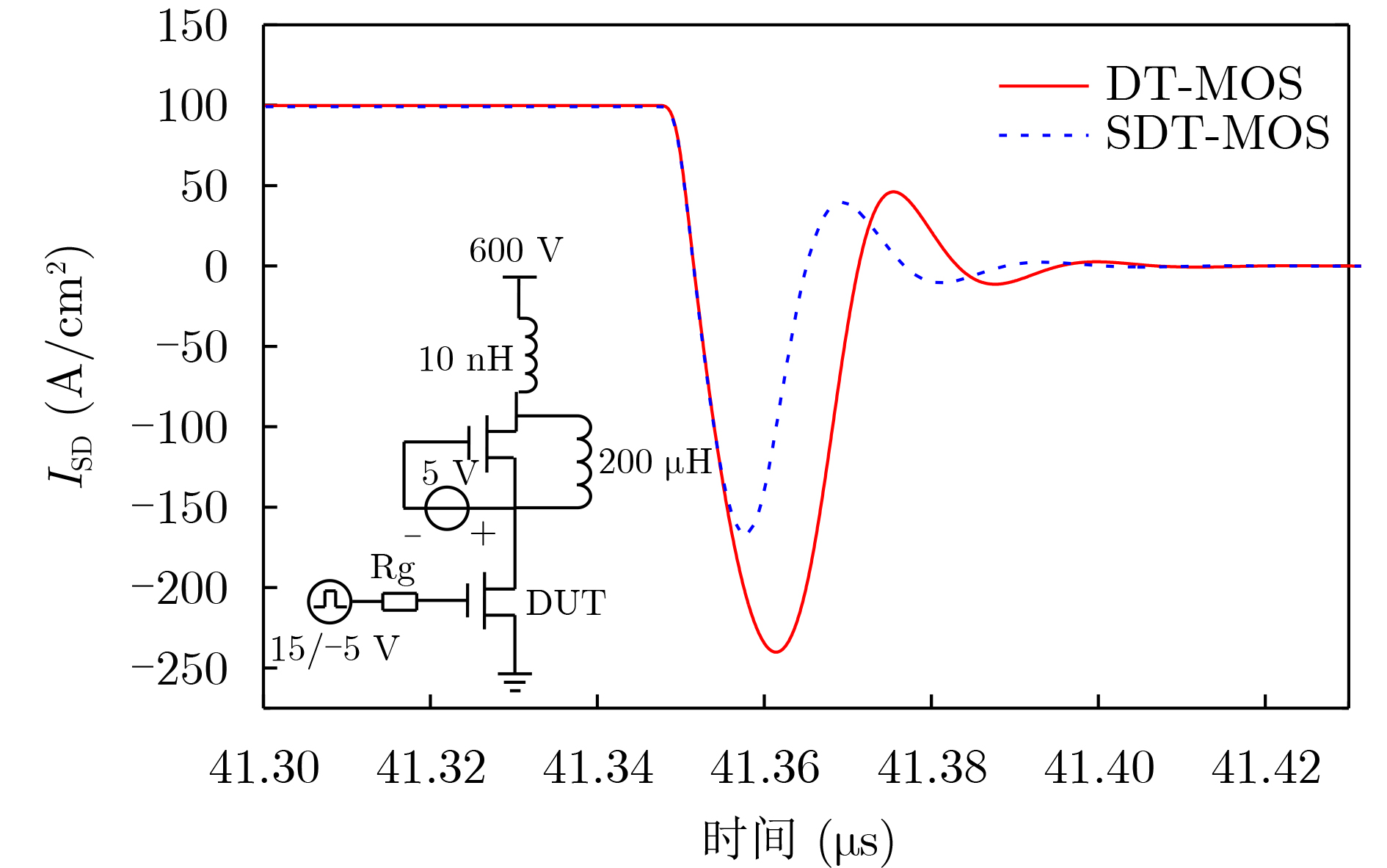
Abstract:This paper proposes a novel double-trench Silicon Carbide (SiC) MOSFET that integrates a Schottky diode structure to improve reverse recovery and switching characteristics. In the proposed design, the conventional right-side trench channel is replaced by a Schottky diode, and a split-gate structure is connected to the source. The Schottky diode suppresses body diode conduction and eliminates the bipolar degradation effect. The split gate reduces the coupling area between the gate and drain, thereby lowering the feedback capacitance and gate charge. In addition, when the split gate is connected to a high potential, it attracts electrons to form an accumulation layer near the source, which increases electron density. During reverse conduction, the current flows through the Schottky diode, while the split gate enhances electron concentration and thus current density. The split-gate structure also shields the gate from the drain, reducing the Gate-Drain Charge (QGD) and improving switching performance. Objective Conventional Double-Trench MOSFETs (DT-MOS) typically require an external anti-parallel diode to function as a freewheeling diode in converter and inverter systems. This necessitates additional module area and increases parasitic capacitance and inductance. Utilizing the body diode as a freewheeling diode could reduce cost and save space. However, this approach presents two major challenges. First, due to the wide bandgap of SiC, the turn-on voltage of the intrinsic body diode rises significantly (approaching 3 V), which increases switching loss. This paper presents a new DT-MOS, referred to as SDT-MOS, with an integrated Schottky diode, demonstrated using TCAD SENTAURUS. In the proposed structure, the conventional right-side channel is replaced with a Schottky junction, and a source-connected split gate is embedded in the gate oxide. The SDT-MOS achieves low power consumption and reduced reverse recovery current. Methods Sentaurus TCAD is used to simulate and analyze the electrical performance of the proposed structure and its conventional counterpart. The simulation includes key physical models, such as mobility saturation under high electric fields, Auger recombination, Okuto-Crowell impact ionization, bandgap narrowing, and incomplete ionization. To improve simulation accuracy and align the results with experimental data, interface traps and fixed charges at the SiC/SiO2 interface are also considered. Results and Discussions The Miller capacitance (Crss or CGD) extracted at VDS of 400 V is 29 pF/cm2 for the SDT-MOS, representing a 61% reduction compared to the DT-MOS, which has a CGD of 74 pF/cm2. This reduction is primarily attributed to the integrated split-gate structure, which decreases the capacitive coupling between the gate and drain electrodes ( Fig. 7 ). The total switching loss (Eon + Eoff) of the SDT-MOS is 1.58 mJ/cm2, which is 59.3% lower than that of the DT-MOS (3.88 mJ/cm2), due to the improved switching characteristics enabled by the split gate (Fig. 10 ). In addition, the peak reverse recovery current (IRRM) and reverse recovery charge (QRR) of the SDT-MOS are 165 A/cm2 and 1.39 μC/cm2, representing reductions of 31.3% and 54%, respectively, compared to the DT-MOS (Fig. 11 ).Conclusions A novel double-trench SiC MOSFET (SDT-MOS) with an integrated Schottky diode has been numerically investigated. In this structure, the right-side channel of a conventional DT-MOS is replaced with a Schottky diode, and a split gate is connected to the source. This configuration results in improved switching and reverse recovery performance. With appropriate optimization of key design parameters, the SDT-MOS retains the fundamental characteristics of a standard MOSFET. Compared with the conventional DT-MOS, the proposed device suppresses body diode conduction, mitigates bipolar degradation, and achieves a 64.9% reduction in QGD. Switching loss is reduced by 59.3%, and QRR is reduced by 54%. These enhancements make the SDT-MOS a strong candidate for high-efficiency, high–power density applications. -
Key words:
- Schottky diode /
- Bipolar degradation effect /
- Split gate
-
表 1 两种器件关键参数
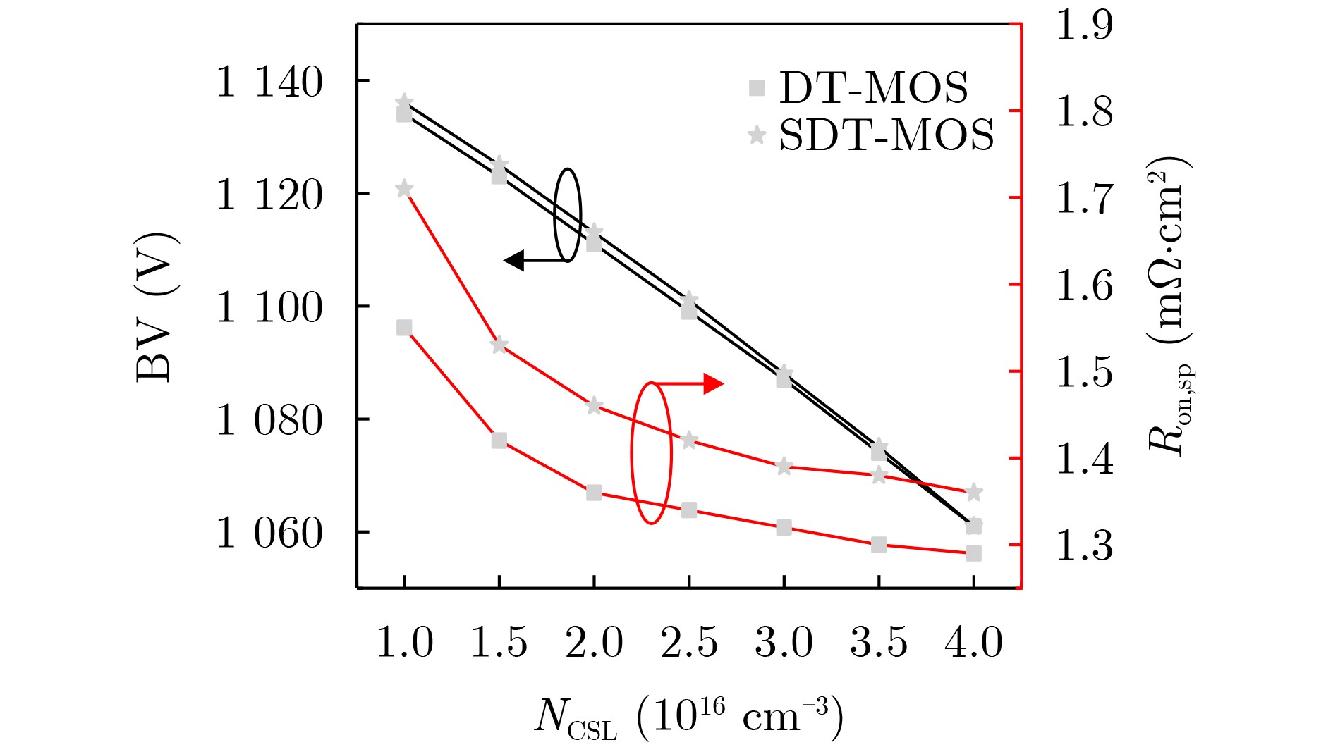
参数 DT-MOS SDT-MOS Cell pitch 3 μm 3 μm TDrift 11 μm 11 μm Wgate 0.9 μm 0.25 μm Tgate 1 μm 1 μm Tox 50 nm 20 nm NDrift 7×1015 cm–3 7×1015 cm–3 NP-base 2.5×1017 cm–3 2.5×1017 cm–3 NCSL 2.5×1016 cm–3 2.5×1016 cm–3 W - 0.3 μm Tox2 - 0.2 μm  下载: 导出CSV
表 2 两种器件的关键性能对比
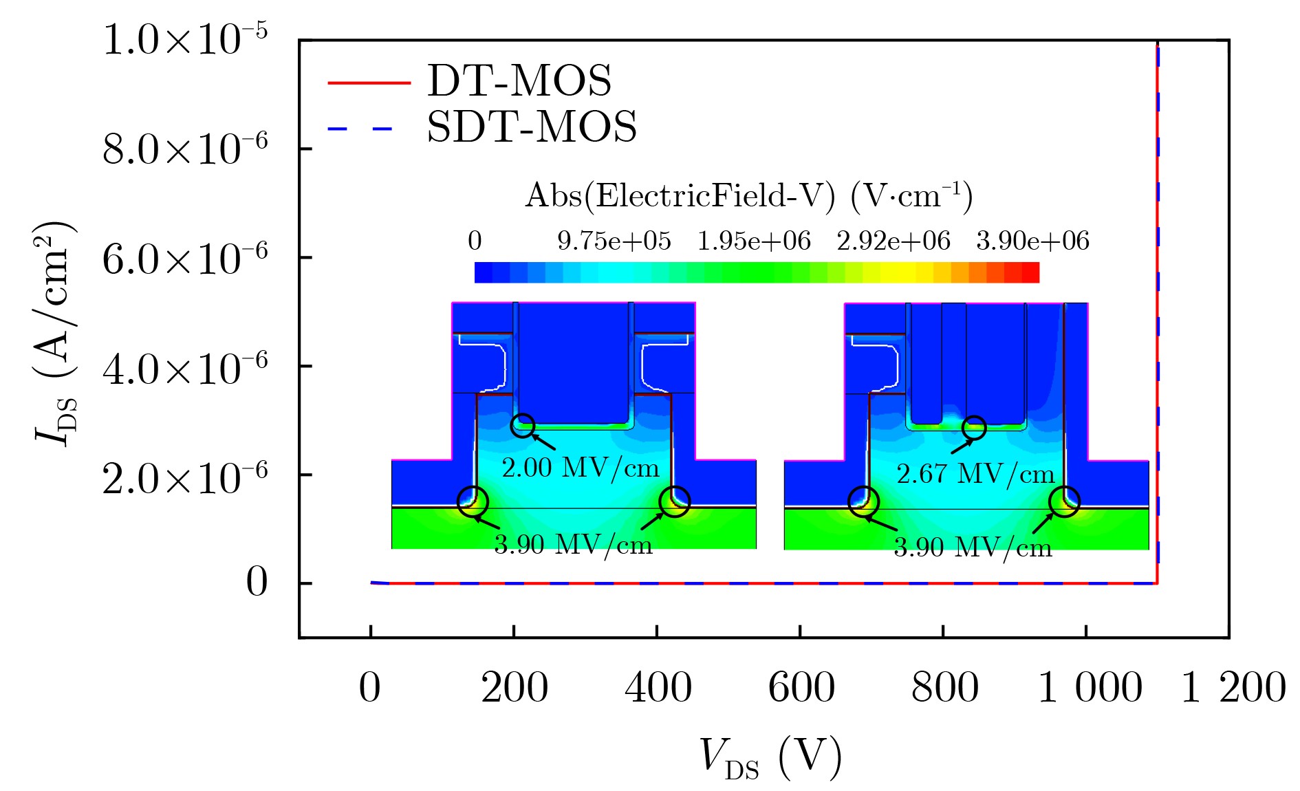
参数 DT-MOS SDT-MOS Vcut-in 2.8 V 1.5 V Ron,sp 1.36 mΩ·cm2 1.41 mΩ·cm2 BV 1 099 V 1 101 V QGD 303 nC/cm2 106.5 nC/cm2 Eon/Eoff 1.96/1.92 mJ/cm2 0.67/0.91 mJ/cm2 QRR 3.02 μC/cm2 1.39 μC/cm2 Ron,sp×CGD 107.4 mΩ·pF 41.2 mΩ·pF Ron,sp×QGD 412.1 mΩ·nC 151.2 mΩ·nC
下载: 导出CSV
-
[1] JIN Miaoixn, GAO Qiang, WANG Yijie, et al. A temperature-dependent SiC MOSFET modeling method based on MATLAB/Simulink[J]. IEEE Access, 2018, 6: 4497–4505. doi: 10.1109/ACCESS.2017.2776898. [2] ZHANG Jinping, ZHANG Bo, and LI Zhaoji. Asymmetric 3D tri-gate 4H-SiC MESFETs with a recessed drain drift region[J]. Semiconductor Science and Technology, 2009, 24(4): 045001. doi: 10.1088/0268-1242/24/4/045001. [3] SHE Xu, HUANG A Q, LUCÍA Ó, et al. Review of silicon carbide power devices and their applications[J]. IEEE Transactions on Industrial Electronics, 2017, 64(10): 8193–8205. doi: 10.1109/TIE.2017.2652401. [4] DENG Xiaochuan, XU Xiaojie, LI Xuan, et al. A novel SiC MOSFET embedding low barrier diode with enhanced third quadrant and switching performance[J]. IEEE Electron Device Letters, 2020, 41(10): 1472–1475. doi: 10.1109/LED.2020.3017650. [5] AN Junjie and HU Shengdong. Heterojunction diode shielded SiC split-gate trench MOSFET with optimized reverse recovery characteristic and low switching loss[J]. IEEE Access, 2019, 7: 28592–28596. doi: 10.1109/ACCESS.2019.2902246. [6] WEI Jin, WANG Yuru, ZHANG Meng, et al. High-speed power MOSFET with low reverse transfer capacitance using a trench/planar gate architecture[C]. Proceedings of 2017 29th International Symposium on Power Semiconductor Devices and IC's, Sapporo, Japan, 2017: 331–334. doi: 10.23919/ISPSD.2017.7988956. [7] YUAN Xibo, LAIRD I, and WALDER S. Opportunities, challenges, and potential solutions in the application of fast-switching SiC power devices and converters[J]. IEEE Transactions on Power Electronics, 2021, 36(4): 3925–3945. doi: 10.1109/TPEL.2020.3024862. [8] LI Helong and MUNK-NIELSEN S. Detail study of SiC MOSFET switching characteristics[C]. Proceedings of 2014 IEEE 5th International Symposium on Power Electronics for Distributed Generation Systems, Galway, Ireland, 2014: 1–5. doi: 10.1109/PEDG.2014.6878691. [9] ISHIGAKI T, MURATA T, KINOSHITA K, et al. Analysis of degradation phenomena in bipolar degradation screening process for SiC-MOSFETs[C]. Proceedings of 2019 31st International Symposium on Power Semiconductor Devices and ICs, Shanghai, China, 2019: 259–262. doi: 10.1109/ISPSD.2019.8757598. [10] PENG Kang, ESKANDARI S, and SANTI E. Characterization and modeling of SiC MOSFET body diode[C]. Proceedings of 2016 IEEE Applied Power Electronics Conference and Exposition, Long Beach, USA, 2016: 2127–2135. doi: 10.1109/APEC.2016.7468161. [11] AGARWAL A, FATIMA H, HANEY S, et al. A new degradation mechanism in high-voltage SiC power MOSFETs[J]. IEEE Electron Device Letters, 2007, 28(7): 587–589. doi: 10.1109/LED.2007.897861. [12] CHEN Yuzhi, LI Chi, WU Yifan, et al. A physical-based 3rd-quadrant behavioral model for power SiC MOSFET[C]. Proceedings of 2023 IEEE 10th Workshop on Wide Bandgap Power Devices & Applications, Charlotte, USA, 2023: 1–6. doi: 10.1109/wipda58524.2023.10382219. [13] DING Jiawei, DENG Xiaochun, LI Songjun, et al. A low-loss diode integrated SiC trench MOSFET for improving switching performance[J]. IEEE Transactions on Electron Devices, 2022, 69(11): 6249–6254. doi: 10.1109/TED.2022.3208802. [14] YU Yiren, LIU Tao, MA Rongyao, et al. A novel asymmetric trench SiC MOSFET with an integrated JFET for improved reverse conduction performance[J]. IEEE Transactions on Electron Devices, 2024, 71(3): 1546–1552. doi: 10.1109/TED.2023.3333285. [15] CALLANAN R, RICE J, and PALMOUR J. Third quadrant behavior of SiC MOSFETs[C]. Proceedings of 2013 Twenty-Eighth Annual IEEE Applied Power Electronics Conference and Exposition, Long Beach, USA, 2013: 1250–1253. doi: 10.1109/apec.2013.6520459. [16] SUNG W and BALIGA B J. On developing one-chip integration of 1.2 kV SiC MOSFET and JBS diode (JBSFET)[J]. IEEE Transactions on Industrial Electronics, 2017, 64(10): 8206–8212. doi: 10.1109/TIE.2017.2696515. [17] JIANG Huaping, WEI Jin, DAI Xiaoping, et al. SiC MOSFET with built-in SBD for reduction of reverse recovery charge and switching loss in 10-kV applications[C]. Proceedings of 2017 29th International Symposium on Power Semiconductor Devices and IC’s, Sapporo, Japan, 2017: 49–52. doi: 10.23919/ISPSD.2017.7988890. [18] MANUAL T S D. TCAD sentaurus device manual[J]. USA, 2013. doi: 10.1201/9781003393542-11. [19] NAKAMURA T, NAKANO Y, AKETA M, et al. High performance SiC trench devices with ultra-low ron[C]. Proceedings of 2011 International Electron Devices Meeting, Washington, USA, 2011: 26.5. 1–26.5. 3. doi: 10.1109/IEDM.2011.6131619. [20] PETERS D, SIEMIENIEC R, AICHINGER T, et al. Performance and ruggedness of 1200V SiC—Trench—MOSFET[C]. Proceedings of 2017 29th International Symposium on Power Semiconductor Devices and IC's, Sapporo, Japan, 2017: 239–242. doi: 10.23919/ISPSD.2017.7988904. [21] KIM D and SUNG W. Improved short-circuit ruggedness for 1.2kV 4H-SiC MOSFET using a deep P-well implemented by channeling implantation[J]. IEEE Electron Device Letters, 2021, 42(12): 1822–1825. doi: 10.1109/LED.2021.3123289. -

 下载:
下载:


图(11) / 表(2)
计量
- 文章访问数: 1052
- HTML全文浏览量: 771
- PDF下载量: 113
- 被引次数: 0
