

A Test Vector CODEC Scheme Based on BRAM-Segmented Synchronous Table Lookup
-
摘要: 基于ATE的集成电路制造测试是芯片产业链的重要一环,而逻辑测试向量的编解码及应用效率,对芯片的测试成本有着重要影响。因此,结合现代FPGA内集成高速BRAM的特点,该文提出一种基于分量统计的测试向量编码方案,用于将被测芯片的全部测试向量生成分量编码表文件。与此同时,设计了一种BRAM分段同步查表控制电路,采用并行单端口BRAM结构多段地址分配模块和写优先访问时序模式,实现测试向量各分量的同步查表和并行输出。该文采用Vivado与Xilinx K7 FPGA开发平台,对查表电路进行了设计和仿真。配置了宽度64 bit和定制分段地址深度的BRAM,结合数据传输和存储地址产生控制逻辑,利用UART接口将分量编码表COE文件下载到目标BRAM中,并取得分量在BRAM中的地址,将其应用于BRAM分段同步查表电路。仿真结果充分验证了同步查表电路功能的正确性。将建议方案用于工程ATE测试板的设计,可以有效提高ATE逻辑测试指令的执行效率。Abstract:
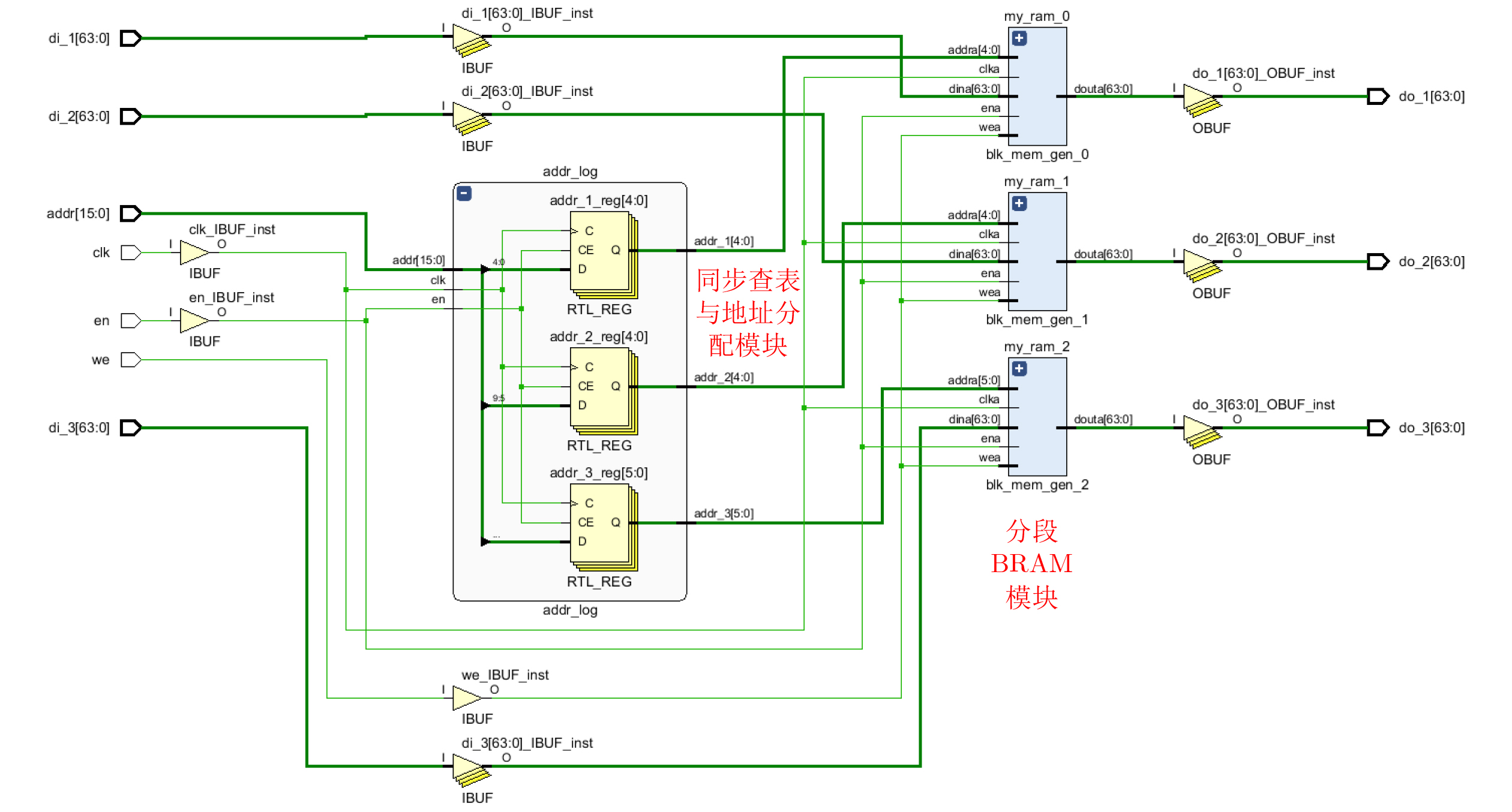
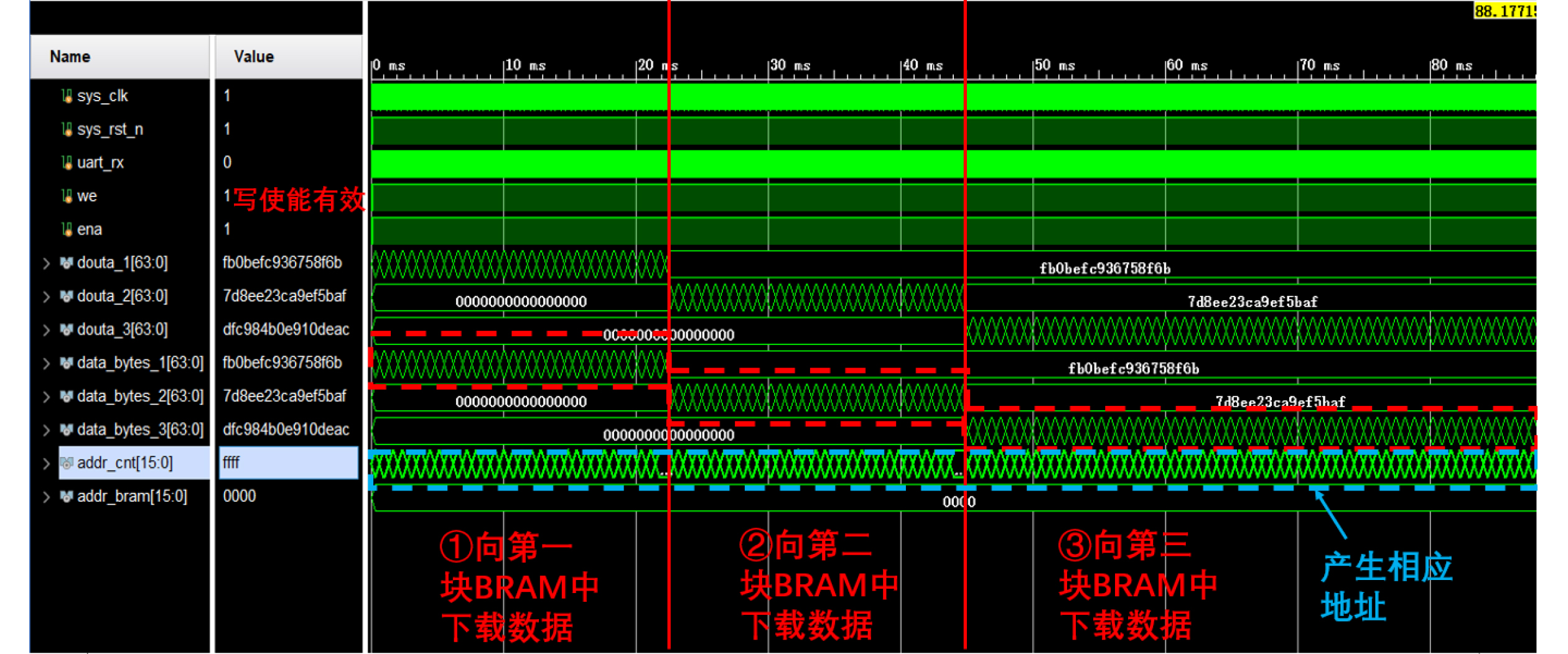
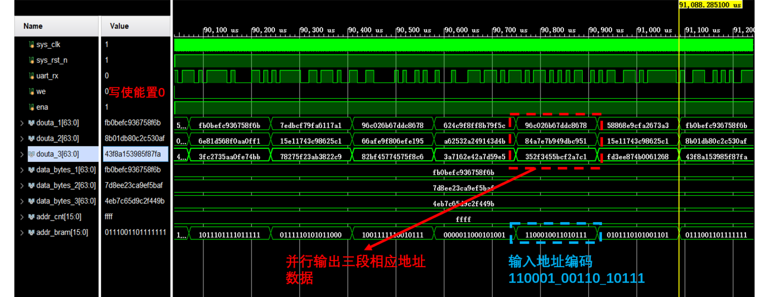
Objective Logic testing using Automatic Test Equipment (ATE) is a critical step in integrated circuit (IC) manufacturing test to ensure chip quality. Enhancing logic test efficiency is essential to reducing digital IC testing costs. During testing, IC test data are typically stored in the main memory of the ATE user board and sequentially read to generate channel test waveforms. The time required to read test data directly affects test efficiency. Traditional Test Data Compression (TDC) approaches, which often require preprocessing such as X-bit filling, are suited only for scan testing and thus do not meet broader test engineering needs. Meanwhile, advances in Field-Programmable Gate Array (FPGA) technology have enabled the customization of high-speed Block RAM (BRAM) resources. This study proposes a test vector coding scheme based on component statistics, in which the Device Under Test (DUT) test vectors are encoded and corresponding component coding tables are generated and stored in the FPGA BRAM. A table lookup circuit is implemented to achieve synchronous, parallel output of all test vector components, effectively reducing the external data read time and improving logic test efficiency. Methods Each bit symbol in an IC test vector comprises four components: drive (DC), measurement (MC), high impedance (ZC), and residual value (RV). The proposed scheme performs statistical encoding of each component across all bit symbols in the DUT’s test vectors and generates shared DC, MC, and ZC coding tables. The encoding process includes: (1) scanning and extracting each vector from the DUT test project files; (2) determining the bit component values and residual values for all channels; (3) for each component, compiling and deduplicating all generated codes, reassigning deleted code references to reserved codes to form the final coding tables; and (4) determining the combined component addresses and residual values. Using a Xilinx Kintex-7 FPGA development board and the Vivado tool, three BRAM modules are configured, and a BRAM table lookup control circuit is designed ( Fig. 4 ). Prior to testing, the component coding tables are downloaded to the FPGA BRAM, and the combined address and residual values of the three component codes for each test vector are stored in off-chip SDRAM. During operation, the lookup circuit uses the combined address to synchronously and in parallel output the three components, which—together with the residual value, drive the waveform generator to produce the channel test waveform.Results and Discussions The functionality of the BRAM-segmented synchronous table lookup circuit is verified through simulation. Three BRAM modules with 64-bit width and customized segment address depth are configured. The COE files of the component encoding tables are downloaded to the target BRAMs via a UART interface, using address generation control logic. The corresponding addresses are then applied to the lookup circuit. A complete simulation is conducted by integrating the segmented lookup module, data strobe module, address allocation module, and data transmission module, enabling validation of the BRAM data download, segmented table lookup, and I/O processes within the FPGA ( Fig. 6 –Fig. 8 ). Results confirm that the synchronized parallel output from the lookup circuit matches the three component codes of the predefined test vectors (Fig. 9 –Fig. 13 ). The SDRAM read time is also analyzed. Under the same configuration parameters, the proposed encoding scheme reduces the read time of each test vector by 66.7% compared with a direct encoding storage scheme (Table 3 ), indicating a significant improvement in logic test efficiency. A qualitative comparison with traditional TDC schemes—including dictionary coding, Frequency-Directed Run-length (FDR) coding and run-length coding, is presented inTable 4 . The results indicate that the proposed scheme, which utilizes high-speed BRAM embedded in modern FPGAs, supports non-scan parallel logic testing with high decoding speed and low overhead, while fully satisfying the original test project requirements.Conclusions A test vector encoding and decoding scheme based on component statistics and BRAM-segmented synchronous table lookup is proposed and implemented. The segmented lookup circuit is designed, and its functional correctness is verified through simulation. Compared with direct encoding, the proposed scheme achieves a 66.7% reduction in logic test time. In contrast to traditional TDC approaches, it offers lower hardware overhead by leveraging embedded high-speed BRAM. The scheme supports ATE-based parallel non-scan logic testing and meets the original engineering design goals, providing a practical foundation for optimizing the logic test function module of the ATE user board. -
Key words:
- Logic test /
- Test vector /
- Component statistical coding /
- BRAM /
- Segmented synchronous table lookup
-
表 1 测试向量位符定义及其编码
位符/
分量驱动 捕获 高阻 残值 含义 DC MC ZC RV 0 1 0 0 0 驱动0 1 1 0 0 1 驱动1 L 0 1 0 0 捕获0 H 0 1 0 1 捕获1 X 0 0 0 0 无关0 W 0 0 0 1 无关1 Z 0 1 1 0 捕获高阻0 Y 0 1 1 1 捕获高阻1 E 1 1 1 0 用于诊断或保留 F 1 1 1 1 C 1 1 0 0 D 1 1 0 1 A 1 0 1 0 B 1 0 1 1 M 0 0 1 0 N 0 0 1 1  下载: 导出CSV
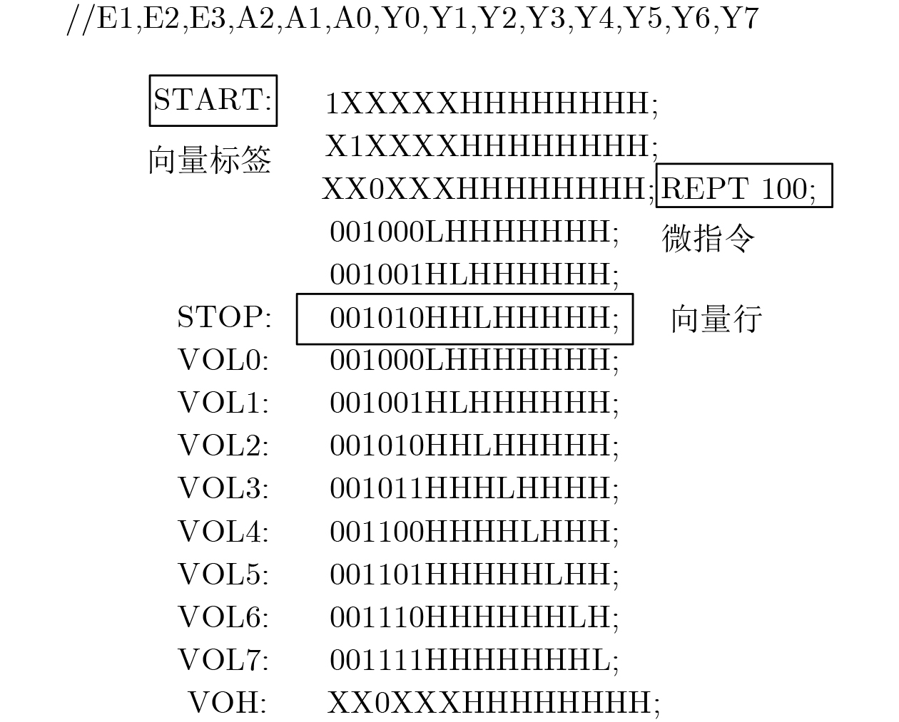
表 2 ATE用户板通道与DUT(74HC138)引脚及其逻辑测试向量配置
ATE CH 16 15 14 13 12 11 10 9 8 7 6 5 4 3 2 1 DUT Pin A0 A1 A2 G2A G2B G1 Y7 Y6 Y5 Y4 Y3 Y2 Y1 Y0 向量1 X X X X X X X X X X X X X X 向量2 1 X X X X X H H H H H H H H 向量3 X 1 X X X X H H H H H H H H 向量4 X X 0 X X X H H H H H H H H 向量5 0 0 1 0 0 0 L H H H H H H H 向量6 0 0 1 0 0 1 H L H H H H H H 向量7 0 0 1 0 1 0 H H L H H H H H 向量8 0 0 1 0 1 1 H H H L H H H H 向量9 0 0 1 1 0 0 H H H H L H H H 向量10 0 0 1 1 0 1 H H H H H L H H 向量11 0 0 1 1 1 0 H H H H H H L H 向量12 0 0 1 1 1 1 H H H H H H H L 向量13 X X X X X X X X X X X X X X
下载: 导出CSV
表 3 与直接编码方案的向量读取延迟比较
方案 原始向量长度(bit) SDRAM存储 (bit) 分量BRAM存储 突发读次数 命令延迟(ns) 访问延迟(ns) 读取延迟(ns) 直接编码 64 4×64+32 无 3 45 120 165 本文 64 32+64+32 有 1 15 40 55
下载: 导出CSV
表 4 与传统编码测试方案的定性比较
代表方案 基本原理 压缩对象 预处理* 解码方式 解码器开销 适用场景 TAT** 工程满足 游程编码[3,4] 部分向量重复次数统计 激励 是 串行解码 较大 串行扫描测试 大 不完全 FDR编码[6,7] 部分向量出现频率统计 激励 是 串行解码 较大 串行扫描测试 大 不完全 字典编码[8–11] 直接向量相容统计 激励 是 串行/并行解码 大 串行扫描测试 较大 不完全 本文 向量分量统计 激励/响应 否 BRAM分段并行查表 小 并行非扫描测试 小 完全 注:*包括对测试集向量的X位填充、重复向量删除、重新排序等,且不可回复,导致原始测试工程目标的不完全满足,**测试应用时间(Test Application Time)
下载: 导出CSV
-
[1] CAREY D R. Introduction to automated test systems–back to basics[C]. IEEE International Automatic Testing Conference (AUTOTESTCON), National Harbor, USA, 2019: 1–7. doi: 10.1109/AUTOTESTCON43700.2019.8961061. [2] 余蓓敏. 高速数电芯片参数测试方案优化研究[J]. 齐齐哈尔大学学报: 自然科学版, 2022, 38(2): 27–31. doi: 10.3969/j.issn.1007-984X.2022.02.006.YU Beimin. Research on parameter test scheme optimization of high speed digital and electrical chip[J]. Journal of Qiqihar University: Natural Science Edition, 2022, 38(2): 27–31. doi: 10.3969/j.issn.1007-984X.2022.02.006. [3] 俞洋, 彭喜元, 张毅刚. 基于重复子向量的测试数据压缩算法[J]. 仪器仪表学报, 2009, 30(2): 356–361. doi: 10.3321/j.issn:0254-3087.2009.02.025.YU Yang, PENG Xiyuan, and ZHANG Yigang. Test data compression method for multiple scan chains based on repeated sub-vectors[J]. Chinese Journal of Scientific Instrument, 2009, 30(2): 356–361. doi: 10.3321/j.issn:0254-3087.2009.02.025. [4] 詹文法, 陶鹏程. 最小游程切换点标记编码压缩方法[J]. 清华大学学报: 自然科学版, 2020, 60(10): 837–844. doi: 10.16511/j.cnki.qhdxxb.2020.26.003.ZHAN Wenfa and TAO Pengcheng. Minimum run-changing point mark coding compression method[J]. Journal of Tsinghua University: Science and Technology, 2020, 60(10): 837–844. doi: 10.16511/j.cnki.qhdxxb.2020.26.003. [5] SSHIMMI S and RAHIMI M. Leveraging code-test co-evolution patterns for automated test case recommendation[C]. The 3rd ACM/IEEE International Conference on Automation of Software Test (AST), Pittsburgh, USA, 2022: 65–76. doi: 10.1145/3524481.3527222. [6] HE Hongxi, HU Jing, LI Zhi, et al. Integrated circuit test data division based on clustering algorithm[C]. The 9th International Conference on Electronic Technology and Information Science (ICETIS), Hangzhou, China, 2024: 604–608. doi: 10.1109/ICETIS61828.2024.10593743. [7] 李瑞. 一种混合分数与FDR码的测试数据压缩方法[D]. [硕士论文], 安庆师范大学, 2022. doi: 10.27761/d.cnki.gaqsf.2022.000029.LI Rui. Test data compression method of mixed fraction and FDR code[D]. [Master dissertation], Anqing Normal University, 2022. doi: 10.27761/d.cnki.gaqsf.2022.000029. [8] JHANCY MABEL D J and VIOLA STELLA MARY M C. A proficient test data compression and decompression system for enhanced test competence in SOC testing[C]. International Conference on Inventive Computation Technologies (ICICT), Lalitpur, Nepal, 2023: 916–920. doi: 10.1109/ICICT57646.2023.10134445. [9] CHEN Rui and XU Lihao. SnappyR: A new high-speed lossless data compression algorithm[C]. Data Compression Conference (DCC), Snowbird, USA, 2023: 334. doi: 10.1109/DCC55655.2023.00052. [10] ROSE J D, DHANUSHKKAR H, and JAGADISHAN M. A self-learning and lossless dictionary-based compression algorithm[C]. IEEE International Conference on Advances in Computing, Communication and Applied Informatics (ACCAI), Chennai, India, 2024: 1–7. doi: 10.1109/ACCAI61061.2024.10601915. [11] CHEN Tian, LIN Chenxin, LIANG Huaguo, et al. A dictionary-based test data compression method using tri-state coding[C]. IEEE 27th Asian Test Symposium (ATS), Hefei, China, 2018: 42–47. doi: 10.1109/ATS.2018.00019. [12] ZHANG Minghe, HUANG Guanglun, JI Guoliang, et al. A scan slice reordering algorithm based on minimizing entropy to enhance test data compression efficiency[C]. IEEE International Test Conference in Asia (ITC-Asia), Changsha, China, 2024: 1–6. doi: 10.1109/ITC-Asia62534.2024.10661362. [13] 李旺康. 基于SOC的测试数据压缩算法研究与分析[D]. [硕士论文], 武汉工程大学, 2023. doi: 10.27727/d.cnki.gwhxc.2023.000658.LI Wangkang. Research on test data compression algorithm based on SOC and analysis[D]. [Master dissertation], Wuhan Institute of Technology, 2023. doi: 10.27727/d.cnki.gwhxc.2023.000658. [14] NIMARA S, BONCALO O, AMARICAI A, et al. FPGA architecture of multi-codeword LDPC decoder with efficient BRAM utilization[C]. IEEE 19th International Symposium on Design and Diagnostics of Electronic Circuits & Systems (DDECS), Kosice, Slovakia, 2016: 1–4. doi: 10.1109/DDECS.2016.7482452. [15] PFEIFER P and PLIVA Z. On utilization of BRAM in FPGA for advanced measurements in mechatronics[C]. IEEE International Workshop of Electronics, Control, Measurement, Signals and their Application to Mechatronics (ECMSM), Liberec, Czech Republic, 2015: 1–6. doi: 10.1109/ECMSM.2015.7208700. [16] MANJULA C and JAYADEVAPPA D. Command driven scalable & programmable FPGA based digital test pattern generator[C]. International Conference on Electrical, Electronics, Communication, Computer, and Optimization Techniques (ICEECCOT), Mysuru, India, 2017: 440–447. doi: 10.1109/ICEECCOT.2017.8284545. [17] ZHANG Xinrui, WANG Jian, WANG Yuan, et al. BRAM-based asynchronous FIFO in FPGA with optimized cycle latency[C]. The 11th IEEE International Conference on Solid-State and Integrated Circuit Technology (ICSSICT), Xi'an, China, 2012: 1–3. doi: 10.1109/ICSICT.2012.6467891. [18] PFEIFER P and PLIVA Z. Delay-fault run-time XOR-less aging detection unit using BRAM in modern FPGAs[C]. The 13th IEEE Biennial Baltic Electronics Conference (BEC), Tallinn, Estonia, 2012: 81–84. doi: 10.1109/BEC.2012.6376820. [19] NG J S, CHEN Juncheng, WU Si, et al. Improving FPGA-based Async-logic AES accelerator with the integration of sync-logic block RAMs[C]. IEEE International Symposium on Circuits and Systems (ISCAS), Monterey, USA, 2023: 1–5. doi: 10.1109/ISCAS46773.2023.10181344. [20] KABIR M D A, HOLLIS J, PANAHI A, et al. Making BRAMs compute: Creating scalable computational memory fabric overlays[C]. IEEE 31st Annual International Symposium on Field-Programmable Custom Computing Machines (FCCM), Marina Del Rey, USA, 2023: 224. doi: 10.1109/FCCM57271.2023.00052. [21] LAI B C C and HUANG Kunhua. An efficient hierarchical banking structure for algorithmic multiported memory on FPGA[J]. IEEE Transactions on Very Large Scale Integration (VLSI) Systems, 2017, 25(10): 2776–2788. doi: 10.1109/TVLSI.2017.2717448. -

 下载:
下载:


图(13) / 表(4)
计量
- 文章访问数: 517
- HTML全文浏览量: 297
- PDF下载量: 33
- 被引次数: 0
