

Calculation and Testing Method of Gap Impedance for X-Band Klystron Multi-Gap Output Cavity
-
摘要: 在雷达与通信系统中,大功率宽频带速调管得到了极为广泛的应用,采用多间隙输出腔体(MGOC)的设计是速调管拓展器件带宽的有效手段,MGOC的间隙阻抗在带内的平坦度直接决定了速调管的带内增益以及带宽,间隙阻抗的计算以及测试方法显示出极端的重要性。该文研究了X波段速调管MGOC的等效电路模型,详细论述了MGOC间隙阻抗的计算方法。另外在微波网络理论的基础上,提出了速调管MGOC间隙阻抗的测试方法。利用以上理论,设计出一种X波段四间隙输出腔,输出段带宽被扩展到1.2 GHz以上。输出段冷测实验件的间隙阻抗测试结果与电路计算结果吻合较好,进一步验证了该方法的有效性。输出段MGOC间隙阻抗的研究为进一步拓展速调管带宽奠定了重要的理论基础。Abstract:
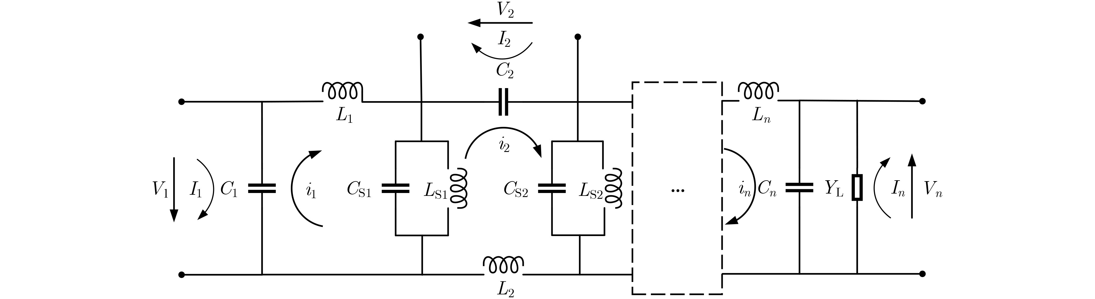
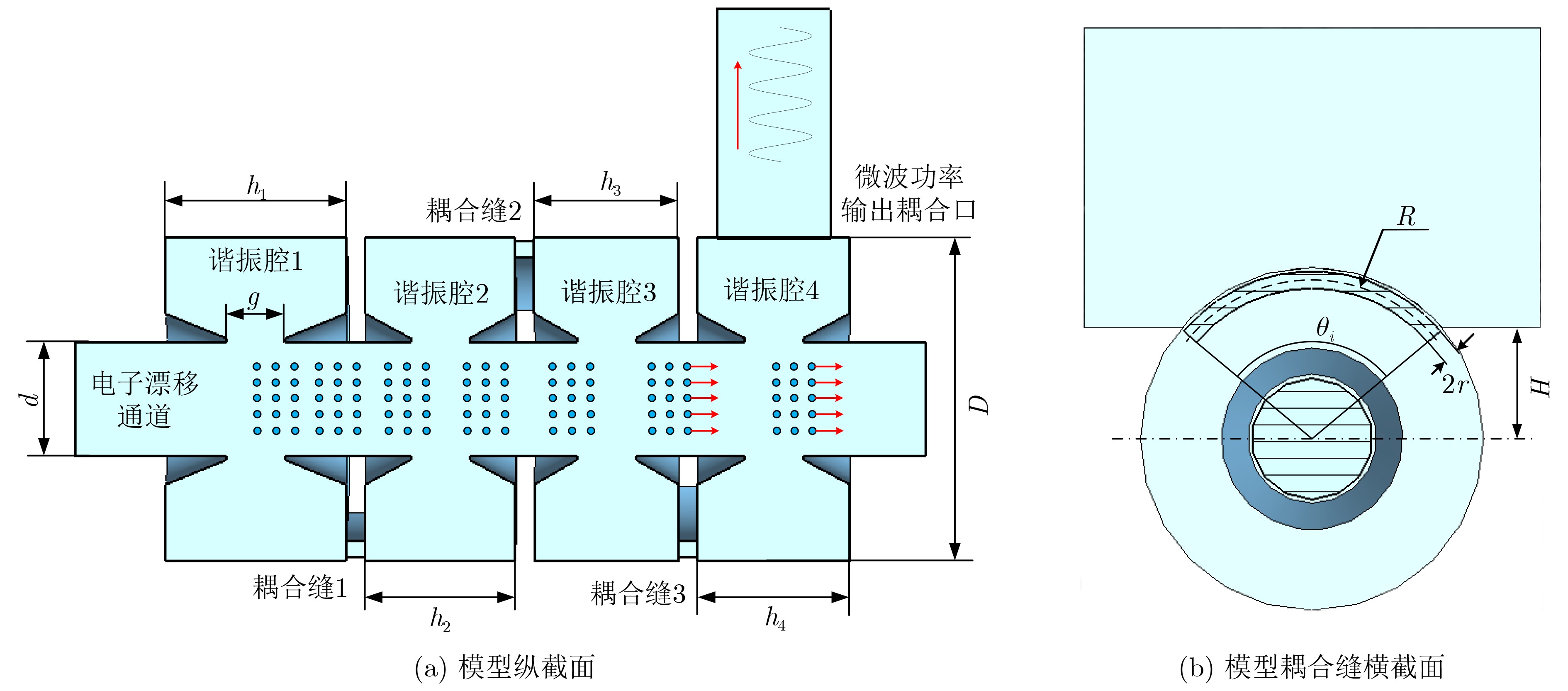
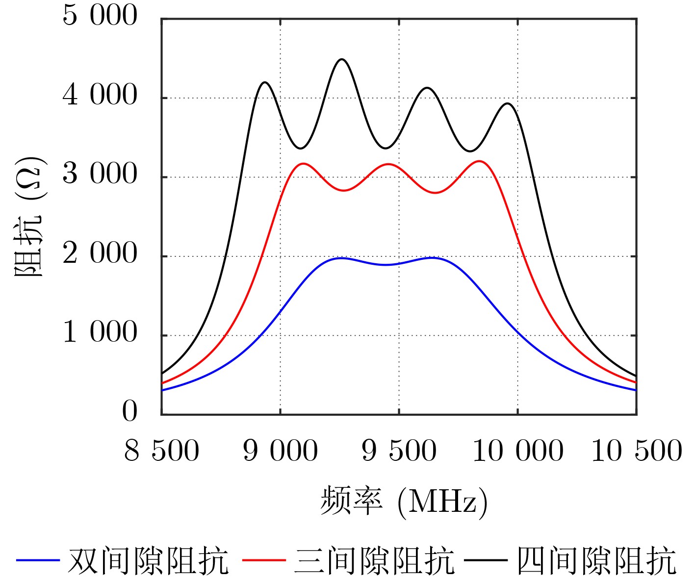
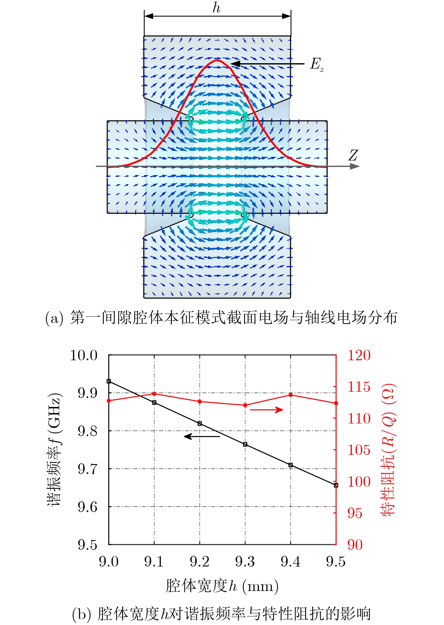
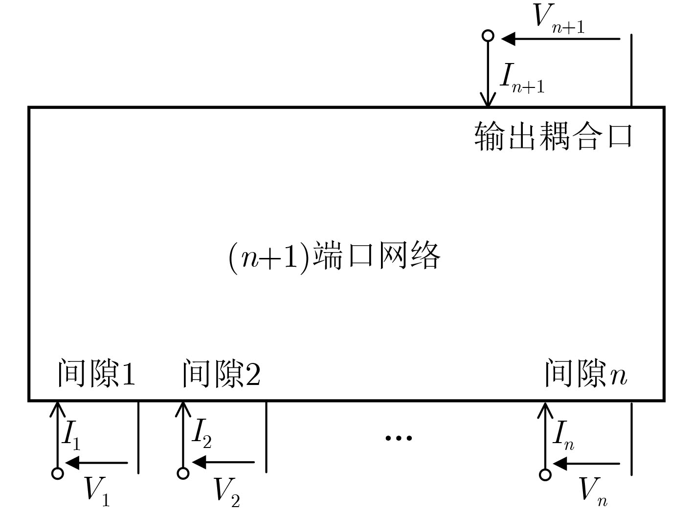
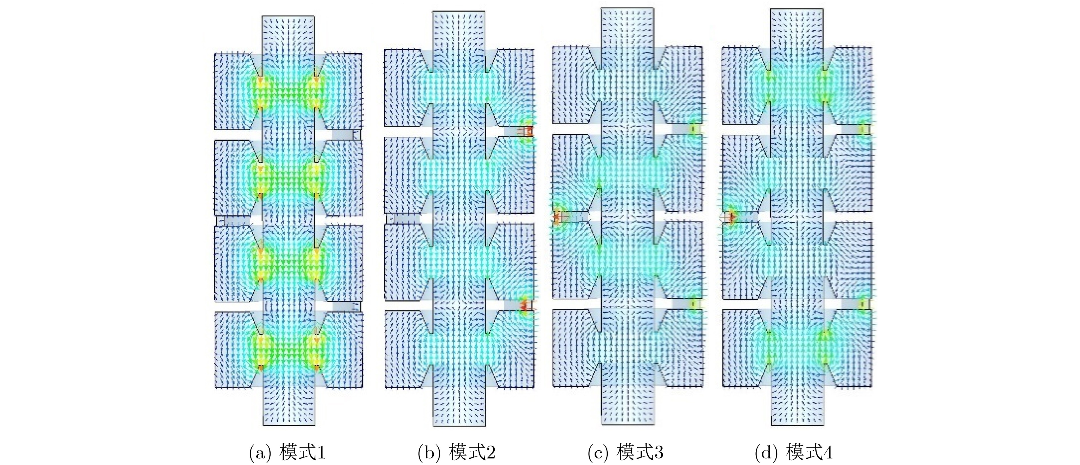
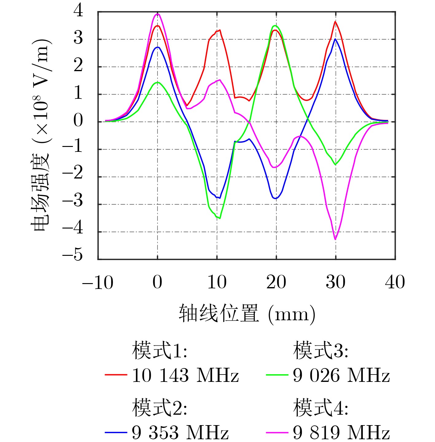
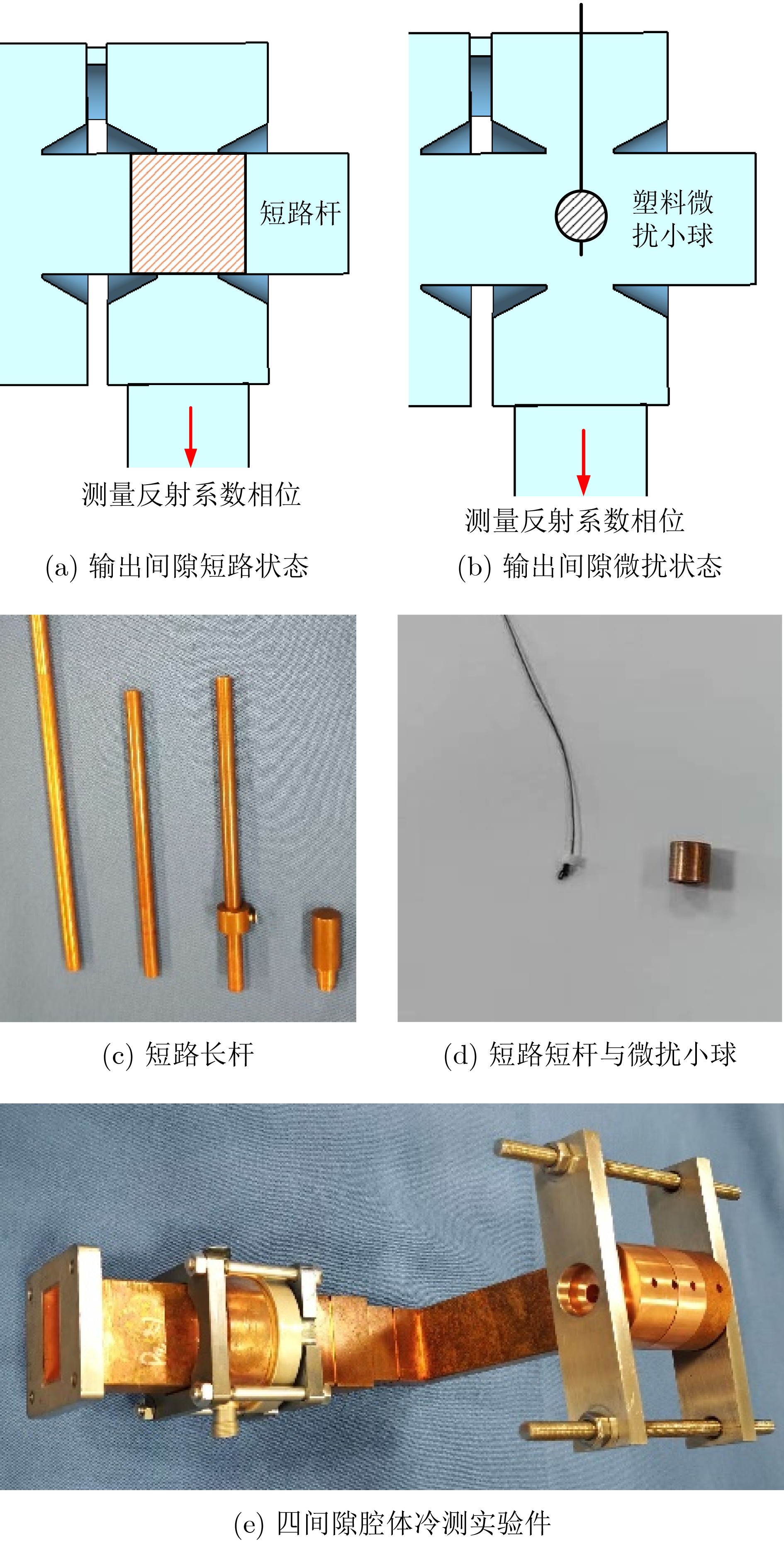
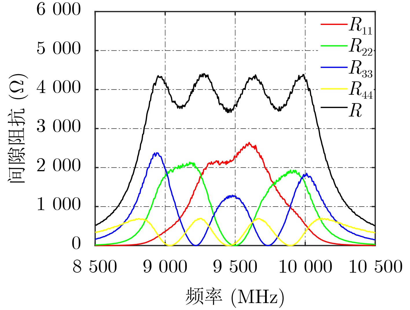
Objective From a structural standpoint, the klystron is a narrowband device that realizes beam-wave interaction through a sequence of independent resonant cavities. Advances in simulation techniques and computational methods for klystrons, as well as advancements in electric vacuum materials, manufacturing processes, and related technologies, have continuously enhanced their power and bandwidth performance. For example, high-power wideband klystrons are now widely applied in radar and communication systems. X-band wideband klystrons have achieved megawatt-level output pulse power, offering substantial utility in a range of radar applications. To satisfy the bandwidth demands of microwave electronic systems, research into wideband klystron technologies is increasingly prioritized. Expanding the bandwidth of the klystron output section is therefore a critical technology in the development of broadband klystrons. Methods Current approaches to expanding the frequency bandwidth of klystrons primarily rely on techniques such as staggered tuning of resonant cavities, integration of waveguide filters at the output cavity, and utilization of overlapping mode configurations in Multi-Gap Output Cavity (MGOC). The output section of high-frequency structures typically adopts a double-gap coupled cavity, for which gap impedance testing methods are relatively well established. Building on this foundation, a triple-gap coupled output cavity structure is developed, enabling further bandwidth enhancement. The flatness of the gap impedance across the operating band of an MGOC directly determines the gain and bandwidth performance of the klystron. Therefore, accurate calculation and testing of gap impedance are essential. This study proposes a method for calculating MGOC impedance based on cavity equivalent circuit theory. The MGOC is modeled as a resonant circuit comprising capacitive and inductive elements, and the gap impedance matrix is derived using the mesh current method. Based on microwave network theory, a corresponding experimental method for measuring MGOC impedance is also proposed. By analyzing the phase of the reflection coefficient at the output coupling port under various conditions—including all gaps open, single-gap short-circuits, and localized perturbations at individual gaps—the gap impedance within the frequency band of the cold test sample is determined. Using this theoretical framework, an X-band four-gap output cavity structure is designed. The gap impedance of the fabricated sample is measured to verify the validity of the proposed method. Results and Discussions The form of the MGOC impedance derived using equivalent circuit theory is presented (Equation 6). The experimental model of the X-band four-gap output cavity is constructed, and the optimized electrical parameters for each cavity are listed ( Table 1 ). The calculated frequency bandwidth over which the internal impedance exceeds3300 Ω in the X-band reaches1200 MHz (Fig. 3 ). This represents a 30% increase compared to the triple-gap cavity and a twofold improvement over the double-gap cavity, meeting the expected design performance. The structural dimensions of the X-band four-gap output cavity are summarized (Table 2 ). A schematic of the MGOC modeled as an (n+1)-port microwave network is shown (Fig. 5 ). By solving for the impedance at the output coupling port, the relationship between the output port and other ports is obtained (Equation 13). The impedance for the all-gaps-open condition is given (Equation 14). The impedance for the case where a single gap is short-circuited and all other gaps remain open is derived (Equation 15), and the impedance corresponding to a perturbation in any single gap capacitance, with the remaining gaps open, is expressed (Equation 16). Based on transmission line theory, the impedance at each gap is calculated using these three sets of expressions (Equations 26~29). Using this theoretical framework, the X-band four-gap cavity prototype is fabricated and tested. To support structural optimization, the four fundamental mode field distributions of the four-gap cavity are first analyzed (Figs. 6 and7 ). The parameters obtained via the equivalent circuit method are refined and adjusted for the cold test component. The final measured impedance distribution of the X-band four-gap cavity is presented (Fig. 9 ). The measured bandwidth, with a gap impedance exceeding3400 Ω, reaches1185 MHz, which closely agrees with the calculated result based on the equivalent circuit model.Conclusions This study proposes a method for calculating the gap impedance of a klystron MGOC based on the mesh current approach within the cavity equivalent circuit framework. A design scheme for an X-band four-gap output cavity is presented, and its impedance bandwidth is compared with those of triple-gap and double-gap cavities. The calculated bandwidth of the four-gap cavity is 33% greater than that of the triple-gap design and twice that of the double-gap counterpart. Building on this, a measurement method for MGOC gap impedance is developed using microwave network theory. Cold test experiments are conducted on an X-band four-gap cavity prototype. The measured results closely match the theoretical predictions, with the impedance exceeding 3400 Ω across nearly 1.2 GHz of bandwidth. Moreover, the proposed cold measurement technique enables the estimation of mutual impedance between cavity gaps by measuring impedance with any two gaps in a short-circuited state. This capability offers important insights into the coupling behavior among cavity modes. These findings provide a robust theoretical and experimental foundation for advancing broadband klystron technologies.-
Key words:
- Klystron /
- Multi-Gap Output Cavity (MGOC) /
- Equivalent circuit /
- Microwave network
-
表 1 X波段双间隙到四间隙输出腔体谐振频率与特性阻抗等参数分布
2 3 4 第1腔体频率 (MHz) 9835 9860 9745 第2腔体频率 (MHz) 9907 10267 10100 第3腔体频率 (MHz) - 10090 10285 第4腔体频率 (MHz) - - 10080 第1耦合缝模频率 (MHz) 13600 15700 15850 第2耦合缝模频率 (MHz) - 15000 16850 第3耦合缝模频率 (MHz) - - 14200 第1腔体特性阻抗 (Ω) 110 110 110 第2腔体特性阻抗 (Ω) 93 110 110 第3腔体特性阻抗 (Ω) - 95 110 第4腔体特性阻抗 (Ω) - - 93 第1耦合缝特性阻抗 (Ω) 7.5 7.5 7 第2耦合缝特性阻抗 (Ω) - 11.5 11.5 第3耦合缝特性阻抗 (Ω) - - 11.5 输出腔外Q 7.2 7.2 7.2  下载: 导出CSV
表 2 四间隙输出腔结构主要几何尺寸
尺寸名称 取值 第1腔腔宽h1 (mm) 9.35 第2腔腔宽h2 (mm) 7.9 第3腔腔宽h3 (mm) 7.6 第4腔腔宽h4 (mm) 8 第1~4腔间隙宽度g (mm) 3.1 第1~4腔直径D (mm) 17 漂移通道直径d (mm) 6 第1~4耦合缝宽度2r (mm) 0.84 第1~4耦合缝中心半径R (mm) 7.88 第1耦合缝张角θ1 100° 第2耦合缝张角θ2 75° 第3耦合缝张角θ3 105° 输出耦合口高度H (mm) 5.5
下载: 导出CSV
-
[1] VARIAN R H and VARIAN S F. A high frequency amplifier and oscillator[J]. Journal of Applied Physics, 1939, 10(2): 140. doi: 10.1063/1.1707284. [2] BEUNAS A, MARCHESIN R, BELLEMERE J C, et al. High-power CW klystron for fusion experiments[J]. IEEE Transactions on Electron Devices, 2009, 56(5): 864–869. doi: 10.1109/TED.2009.2015807. [3] STRINGALL R L, RUSSELL D L, and LEBACQZ J V. Klystrons for accelerator improvements[J]. IEEE Transactions on Nuclear Science, 1973, 20(3): 369–372. doi: 10.1109/TNS.1973.4327122. [4] CORMIER R A and MIZUHARA A. 250 kW CW klystron amplifier for planetary radar[J]. IEEE Transactions on Microwave Theory and Techniques, 1992, 40(6): 1056–1062. doi: 10.1109/22.141335. [5] SHABAZIAN A, WRIGHT E L, BATRA R, et al. Development and production of a high-power S-band MSDC klystron for satellite digital radio[C]. 3rd IEEE International Vacuum Electronics Conference, Monterey, USA, 2002: 326–327. doi: 10.1109/IVELEC.2002.999403. [6] 沈宝丽, 王勇, 张兆传, 等. S波段宽带高平均功率速调管群聚段的研制[J]. 微波学报, 2010, 26(S1): 488–490. doi: 10.14183/j.cnki.1005-6122.2010.s1.025.SHEN Baoli, WANG Yong, ZHANG Zhaochuan, et al. Investigation on the S-band broadband high average power klystron’s bunch structure[J]. Journal of Microwaves, 2010, 26(S1): 488–490. doi: 10.14183/j.cnki.1005-6122.2010.s1.025. [7] 丁耀根, 陆孝厚. 具有两节滤波器的速调管宽带输出段的设计方法[J]. 电子与信息学报, 1982, 4(3): 168–174.DING Yaogen and LU Xiaohou. Design considerations of the two-stage-filter type output circuit of broadband klystrons[J]. Journal of Electronics, 1982, 4(3): 168–174. [8] CAI J C, XU J, CHEN S, et al. Advanced theoretical models for broadband klystron development[J]. IEEE Transactions on Electron Devices, 2022, 69(11): 6310–6317. doi: 10.1109/TED.2022.3204519. [9] 黄传禄, 丁耀根, 王勇, 等. 多间隙耦合腔注波互作用计算分析[J]. 真空科学与技术学报, 2012, 32(7): 605–610. doi: 10.3969/j.issn.1672-7126.2012.07.12.HUANG Chuanlu, DING Yaogen, WANG Yong, et al. Calculation and analysis of beam-wave interactions in multi-gap coupled cavity[J]. Chinese Journal of Vacuum Science and Technology, 2012, 32(7): 605–610. doi: 10.3969/j.issn.1672-7126.2012.07.12. [10] WANG Yong, DING Yaogen, LIU Pukun, et al. Development of an S-band klystron with bandwidth of more than 11%[J]. IEEE Transactions on Plasma Science, 2006, 34(3): 572–575. doi: 10.1109/TPS.2006.875782. [11] NGUYEN K T, PERSHING D E, ABE D K, et al. Bandwidth extension of an S-band, fundamental-mode eight-beam klystron[J]. IEEE Transactions on Plasma Science, 2006, 34(3): 576–583. doi: 10.1109/TPS.2006.875768. [12] NGUYEN K T, WRIGHT E L, PERSHING D E, et al. Broadband high-power 18-beam S-band klystron amplifier design[J]. IEEE Transactions on Electron Devices, 2009, 56(5): 883–890. doi: 10.1109/TED.2009.2015411. [13] XU Shouxi, ZHANG Jian, DING Yaogen, et al. Improvement for an S-Band broadband klystron[J]. IEEE Transactions on Electron Devices, 2024, 71(3): 2122–2125. doi: 10.1109/TED.2024.3354871. [14] DING Yaogen, ABE D K, SHEN Bin, et al. An overview of multibeam klystron technology[J]. IEEE Transactions on Electron Devices, 2023, 70(6): 2656–2665. doi: 10.1109/TED.2023.3244906. [15] LIANG Yuan, GU Honghong, and SHEN Bin. Study on electron optics system and oscillation suppression of an X-band multibeam klystron[J]. IEEE Transactions on Electron Devices, 2024, 71(10): 6362–6367. doi: 10.1109/TED.2024.3440953. [16] ZHAO Yongxiang. An impedance measurement method for double-gap klystron cavity[J]. IEEE Transactions on Electron Devices, 1982, 29(2): 316–320. doi: 10.1109/T-ED.1982.20702. [17] GU Honghong, DING Yaogen, SHEN Bin, et al. The design and performance of an X-band broadband klystron with peak power of 1MW[C]. 2023 24th International Vacuum Electronics Conference, Chengdu, China, 2023: 1–2. doi: 10.1109/IVEC56627.2023.10157415. [18] DUBEY G, RAO V S, MAHTO M, et al. Analysis of the dual side-coupled RF cavities for the HPM devices—an equivalent circuit approach[J]. IEEE Transactions on Electron Devices, 2022, 69(4): 2051–2057. doi: 10.1109/TED.2022.3152473. [19] 丁耀根. 大功率速调管的理论与计算模拟[M]. 北京: 国防工业出版社, 2008: 332–333.DING Yaogen. Theory and Computer Simulation of High Power Klystron[M]. Beijing: National Defense Industry Press, 2008: 332–333. [20] GUO Xin, GU Honghong, DING Yaogen, et al. Design of triple-gap cavity output circuit for X band klystron[C]. 2022 23rd International Vacuum Electronics Conference, Monterey, USA, 2022: 422–423. doi: 10.1109/IVEC53421.2022.10292265. -


图(9) / 表(2)
计量
- 文章访问数: 551
- HTML全文浏览量: 368
- PDF下载量: 26
- 被引次数: 0
 下载:
下载:
