Research Progress of Inverse Lithography Technology
-
摘要: 反演光刻技术(ILT)相比传统的光学临近效应修正(OPC),生成的掩模具有成像效果更好,工艺窗口更大等优点,在当前芯片制造的工艺尺寸不断减小的背景下,逐渐成为主流的光刻掩模修正技术。该文首先介绍了反演光刻算法的基本原理和几种主流实现方法;其次,调研了当前反演光刻技术应用在光刻掩模优化问题上的研究进展,分析了反演光刻技术的优势和存在的问题。以希望为计算光刻及相关研究领域的研究人员提供参考,为我国先进集成电路产业的发展提供技术支持。Abstract:
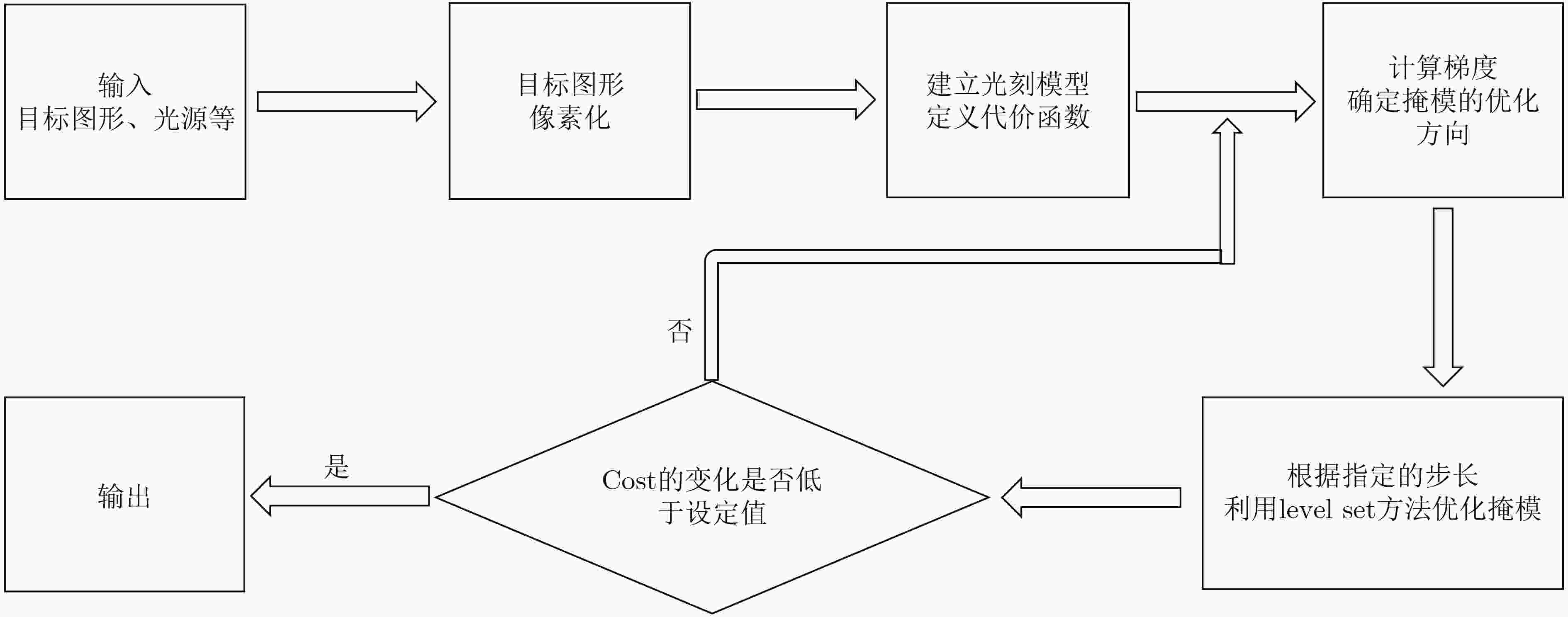
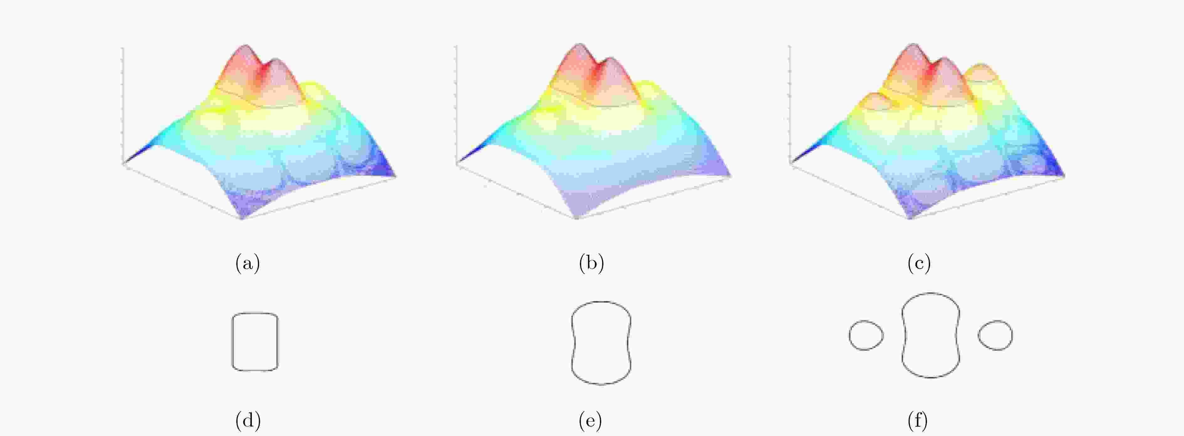
Objective Inverse Lithography Technology (ILT) provides improved imaging effects and a larger process window compared to traditional Optical Proximity Correction (OPC). As chip manufacturing continually reduces process dimensions, ILT has become the leading lithography mask correction technology. This paper first introduces the basic principles and several common implementation methods of the reverse lithography algorithm. It then reviews current research on using reverse lithography technology to optimize lithography masks, as well as analyzes the advantages and existing challenges of this technology. Methods The general process of generating mask patterns in ILT is exemplified using the level set method. First, the target graphics, light sources, and other inputs are identified. Then, the initial mask pattern is created and a pixelated model is constructed. A photolithography model is then established to calculate the aerial image. The general photoresist threshold model is represented by a sigmoid function, which helps derive the imaging pattern on the photoresist. The key element of the ILT algorithm is the cost function, which measures the difference between the wafer image and the target image. The optimization direction is determined based on the chosen cost function. For instance, the continuous cost function can calculate gradients, enabling the use of gradient descent to find the optimal solution. Finally, when the cost function reaches its minimum, the output mask is generated. Results and Discussions This paper systematically introduces several primary methods for implementing ILT. The level set method’s main concept is to convert a two-dimensional closed curve into a three-dimensional surface. Here, the closed curve is viewed as the set of intersection lines between the surface and the zero plane. During the ILT optimization process, the three-dimensional surface shape remains continuous. This continuity allows the ILT problem to be transformed into a multivariate optimization problem, solvable using gradient algorithms, machine learning, and other methods. Examples of the level set method’s application can be found in both mask optimization and light source optimization. The level set mathematical framework effectively addresses two-dimensional curve evolution. When designing the ILT algorithm, a lithography model determines the optimization direction and velocity for each mask point, employing the level set for mask evolution. Intel has proposed an algorithm that utilizes a pixelated model to optimize the entire chip. However, this approach incurs significant computational costs, necessitating larger mask pixel sizes. Notably, the pixelated model is consistently used throughout the process, with a defined pixelated cost function applicable to multi-color masks. The frequency domain method for calculating the ILT curve involves transforming the mask from the spatial domain into the frequency domain, followed by lithography model calculations. This approach generates a mask with continuous pixel values, which is then gradually converted into a binary mask through multiple steps. When modifying the cost function in frequency domain optimization, all symmetric and repetitive patterns are altered uniformly, preserving symmetry. The transition of complex convolution calculations into multiplication processes within the frequency domain significantly reduces computational complexity and can be accelerated using GPU technology. Due to the prevalent issue of high computational complexity in various lithography mask optimization algorithms, scholars have long pursued machine learning solutions for mask optimization. Early research often overlooked the physical model of photolithography technology, training neural networks solely based on optimized mask features. This oversight led to challenges such as narrow process windows. Recent studies have, however, integrated machine learning with other techniques, enabling the physical model of lithography technology to influence neural network training, resulting in improved optimization results. While the ILT-optimized mask lithography process window is relatively large, its high computational complexity limits widespread application. Therefore, combining machine learning with the ILT method represents a promising research direction. Conclusions Three primary techniques exist for optimizing masks using ILT: the Level Set Method, Intel Pixelated ILT Method, and Frequency Domain Calculation of Curve ILT. The Level Set Method reformulates the ILT challenge into a multivariate optimization issue, utilizing a continuous cost function. This approach allows for the application of established methods like gradient descent, which has attracted significant attention and is well-documented in the literature. In contrast, the Intel method relies entirely on pixelated models and pixelated cost functions, though relevant literature on this method is limited. Techniques in the frequency domain can leverage GPU operations to substantially enhance computational speed, and advanced algorithms also exist for converting curve masks into Manhattan masks. The integration of ILT with machine learning technologies shows considerable potential for development. Further research is necessary to effectively reduce computational complexity while ensuring optimal results. Currently, ILT technology faces challenges such as high computational demands and obstacles in full layout optimization. Collaboration among experts and scholars in integrated circuit design and related fields is essential to improve ILT computational speed and to integrate it with other technologies. We believe that as research on ILT-related technologies advances, it will play a crucial role in helping China’s chip industry overcome technological bottlenecks in the future. -
图 3 Level set方法生成SRAF示意图[48]
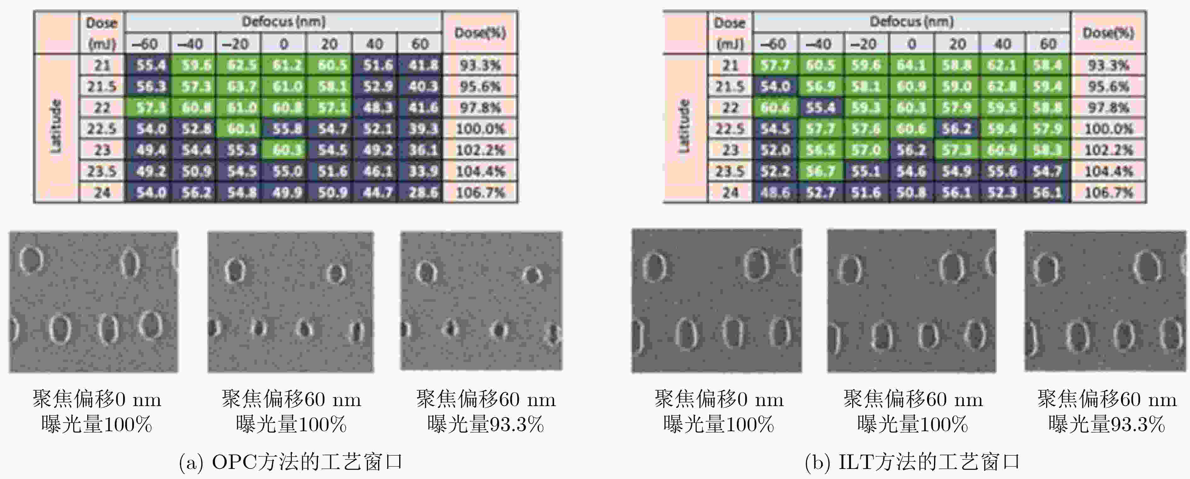
图 5 使用OPC和ILT优化45 nm FLASH的结果[50]
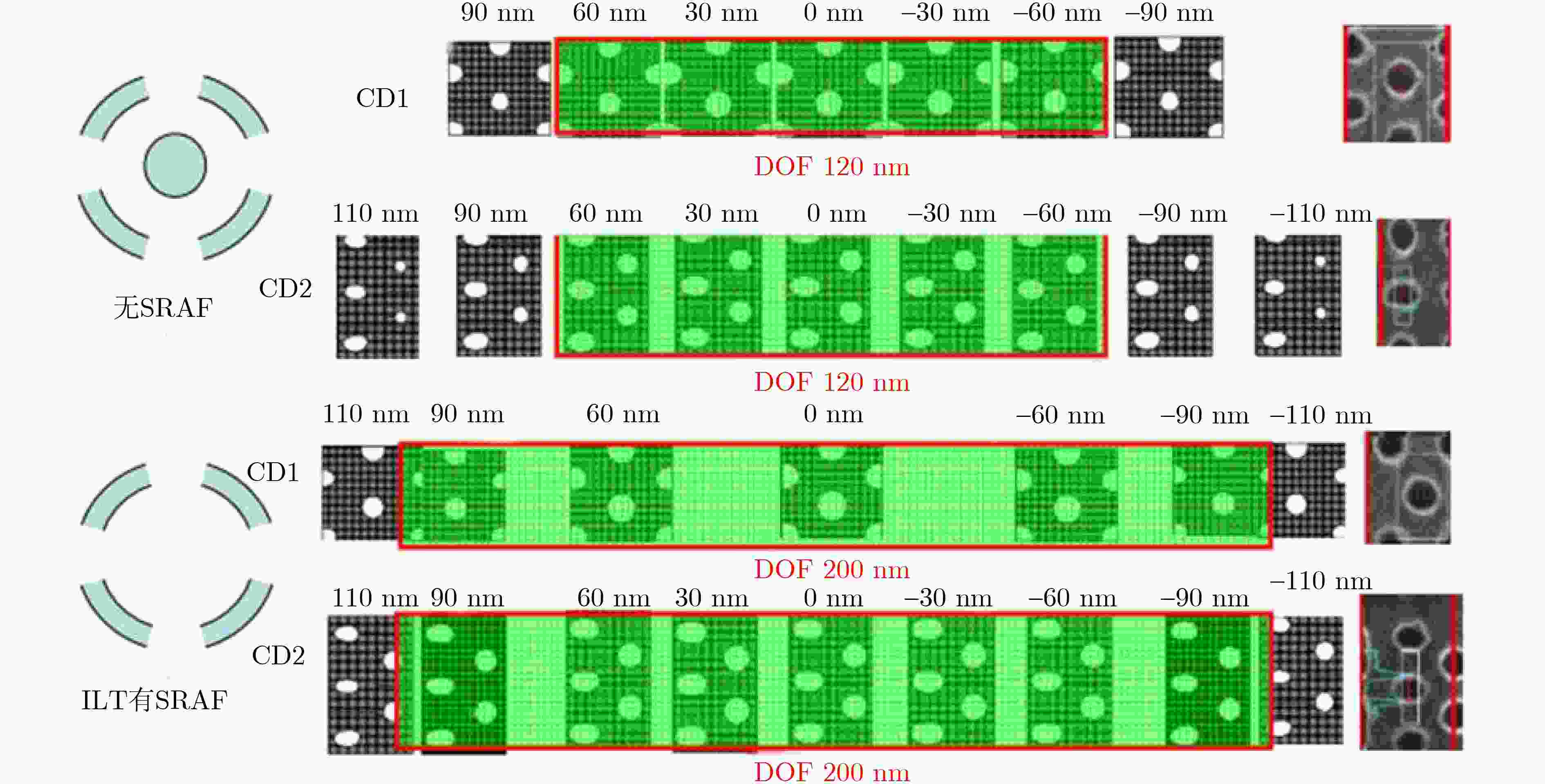
图 6 使用OPC(未插入SRAF)和ILT(插入SRAF)优化45 nm SRAM连接层[50]
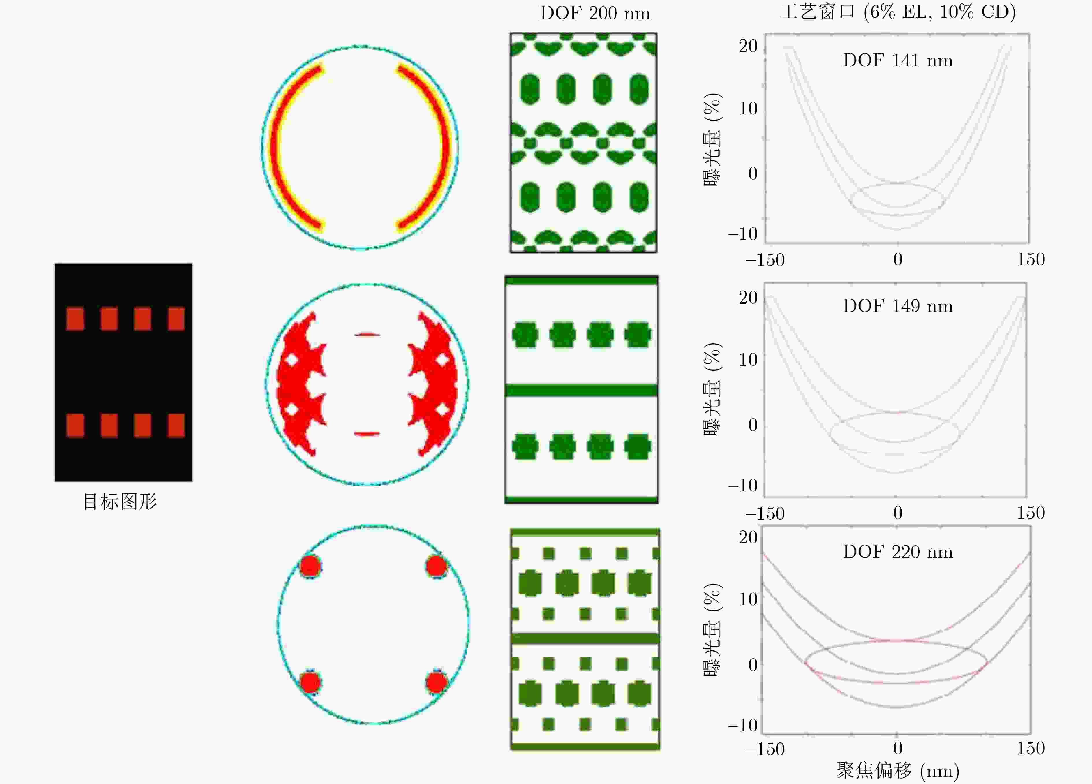
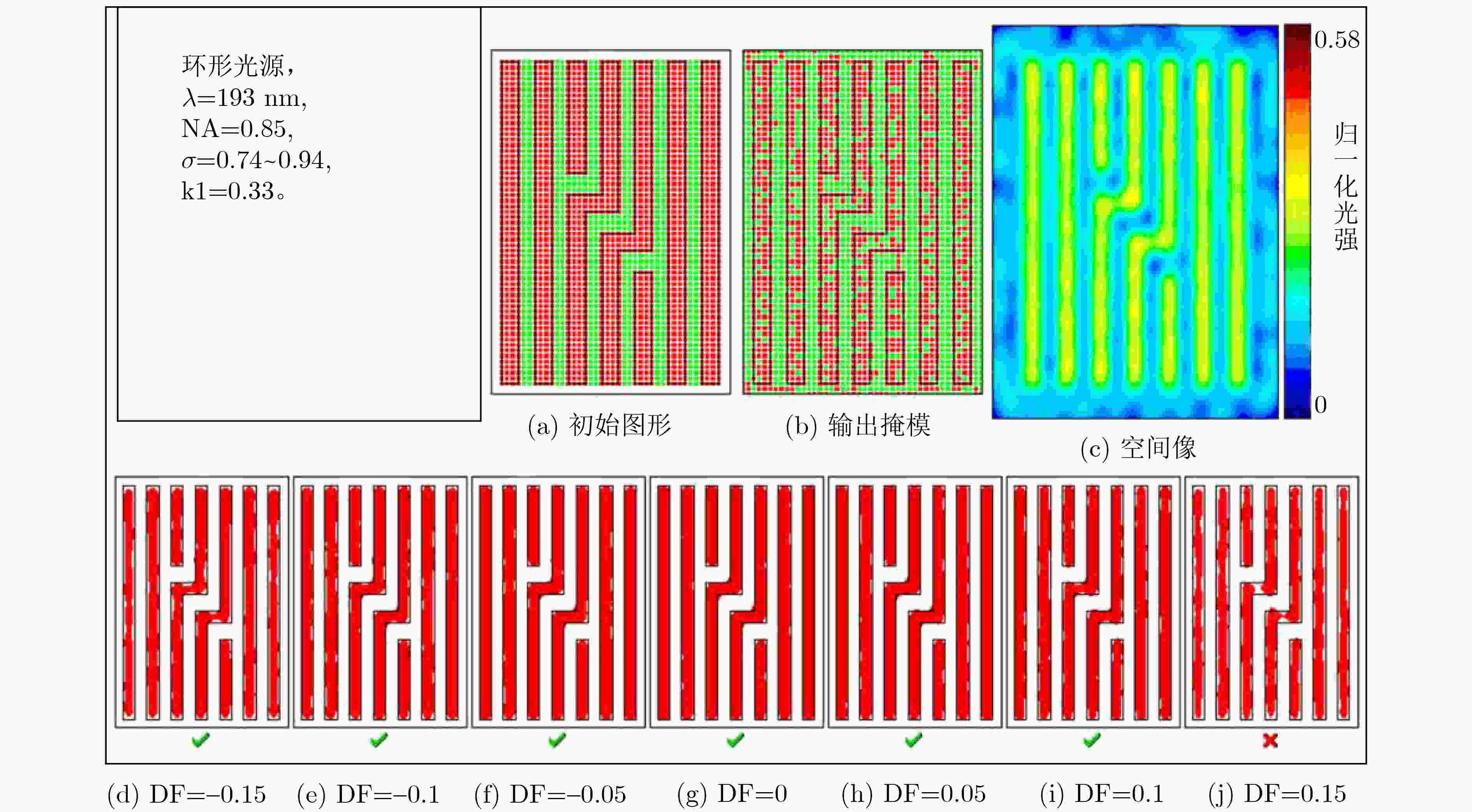
图 7 相同目标图形在不同光源下利用Level set ILT方法生成的掩模图形[50]
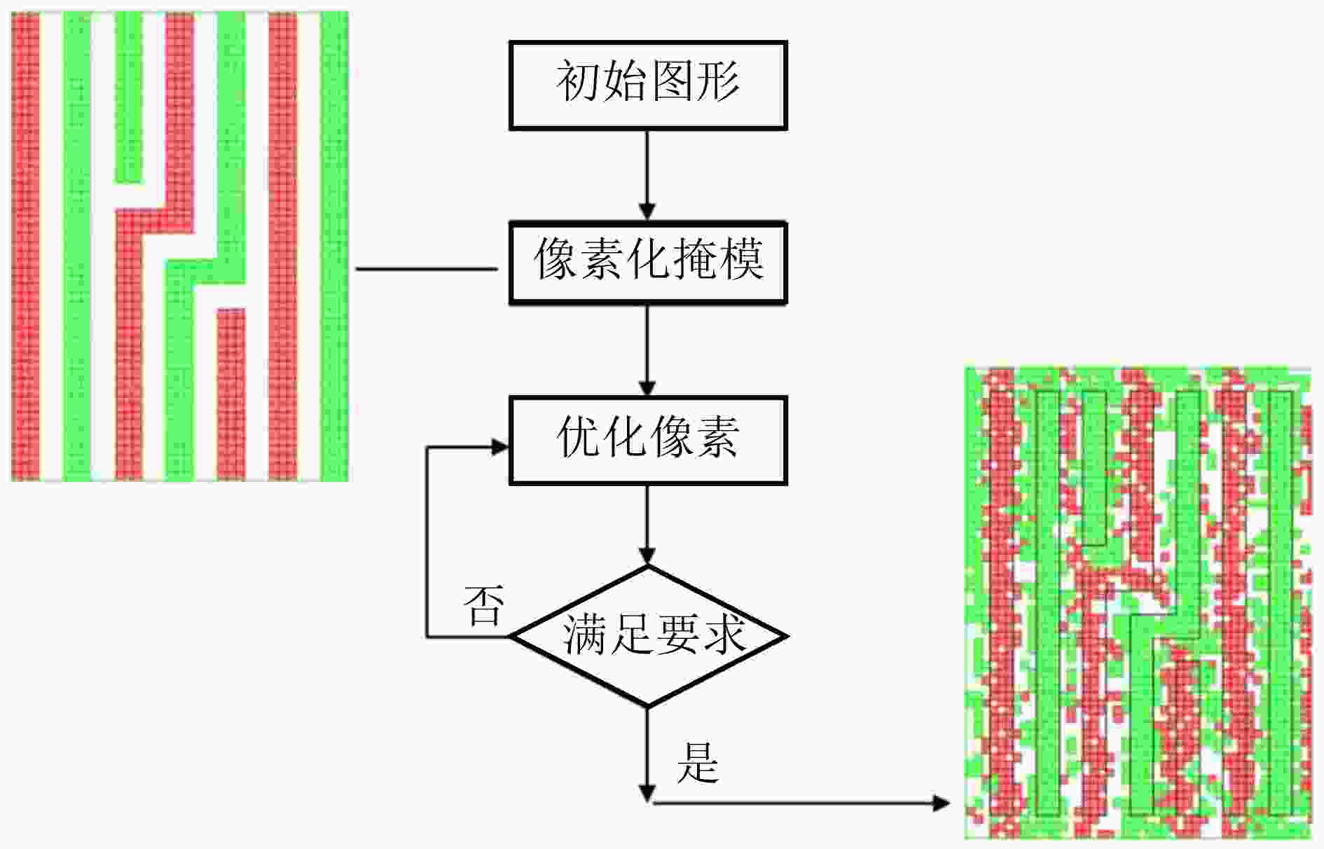
图 8 Intel像素化ILT流程示意图[51]
图 9 Intel像素化ILT双色掩模优化结果[51]
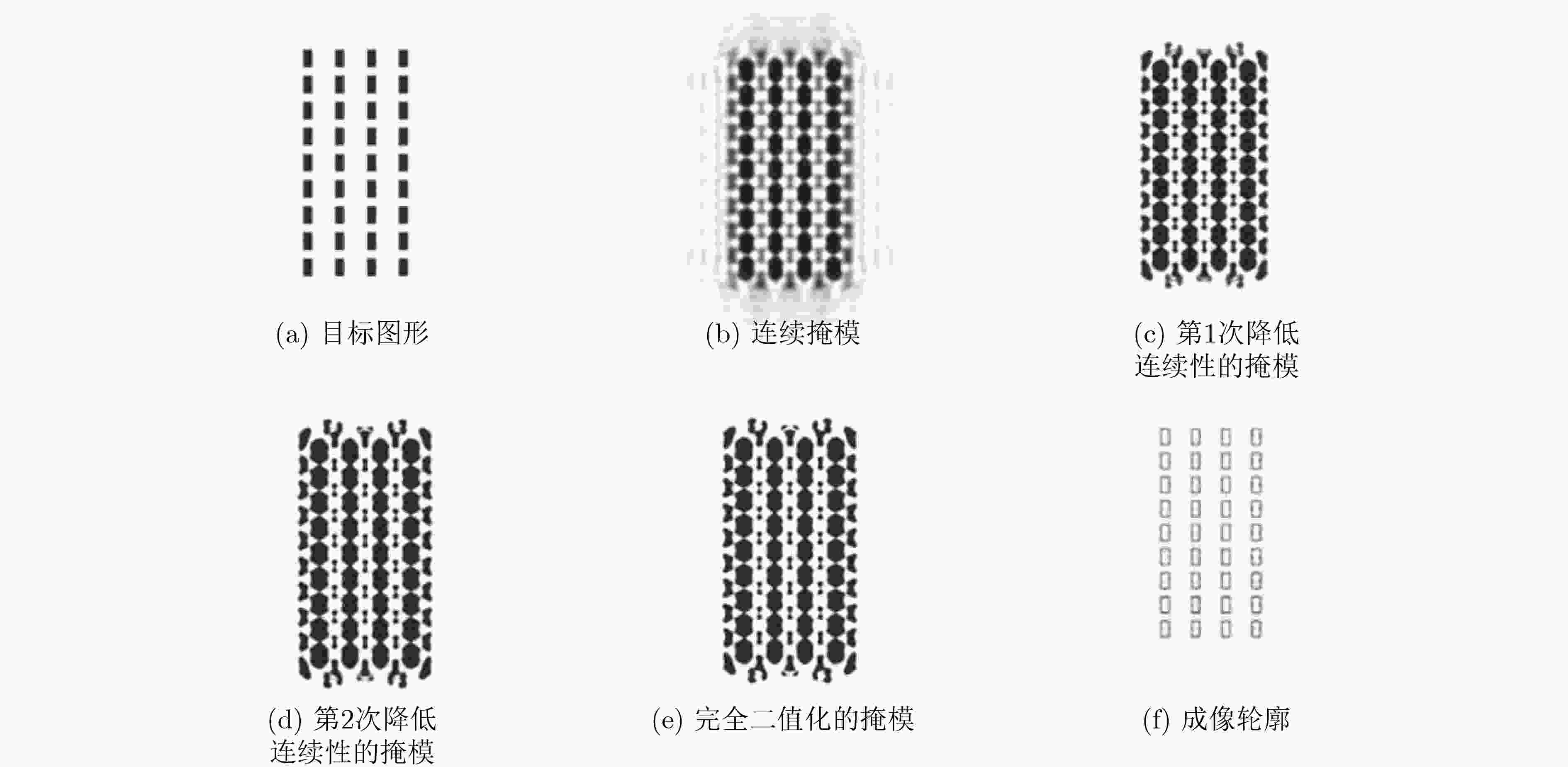
图 10 连续的像素化掩模二值化过程[10]
图 11 OPC与频域中计算曲线 ILT方法的对比[52]
图 12 基于梯度的ILT计算流程示意图[66]
图 13 模型驱动神经网络方法示意图[66]
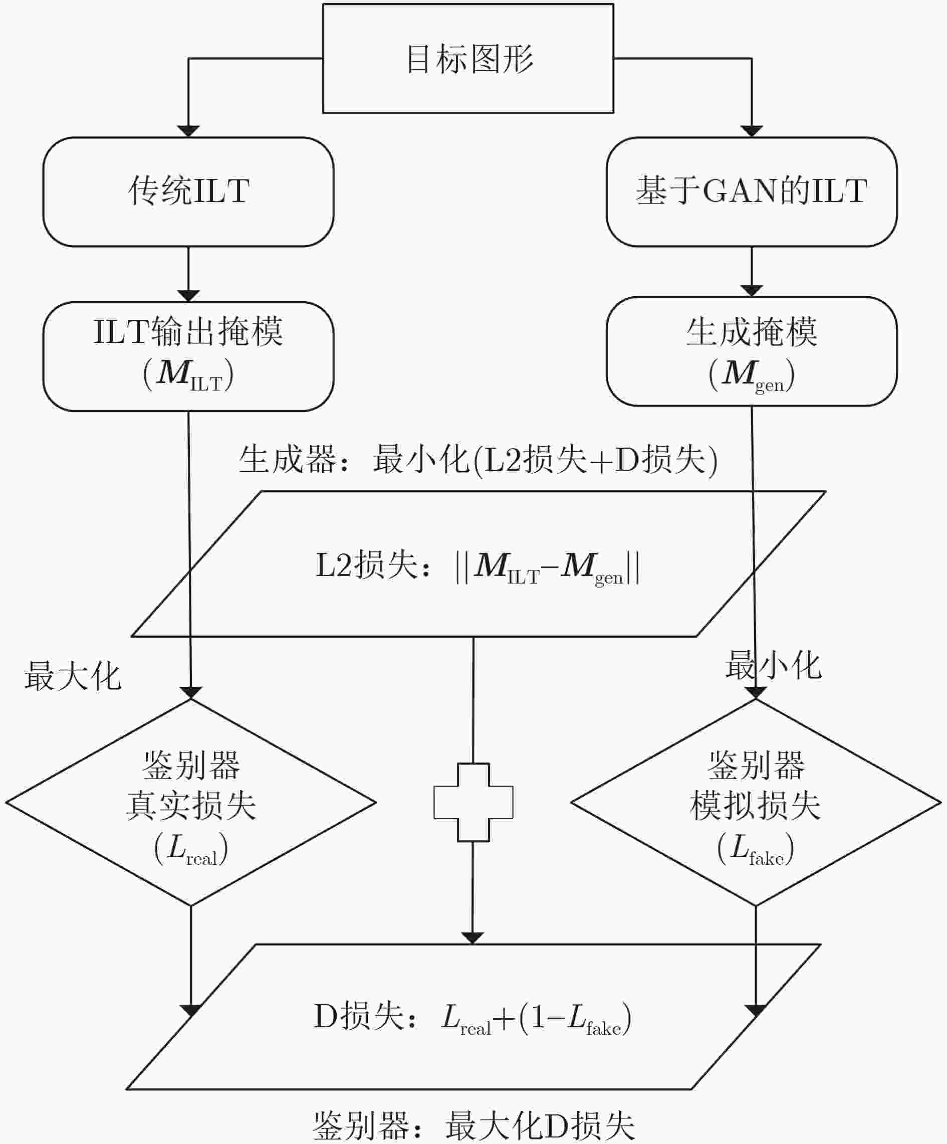
图 14 一种基线CGAN ILT框架图[70]
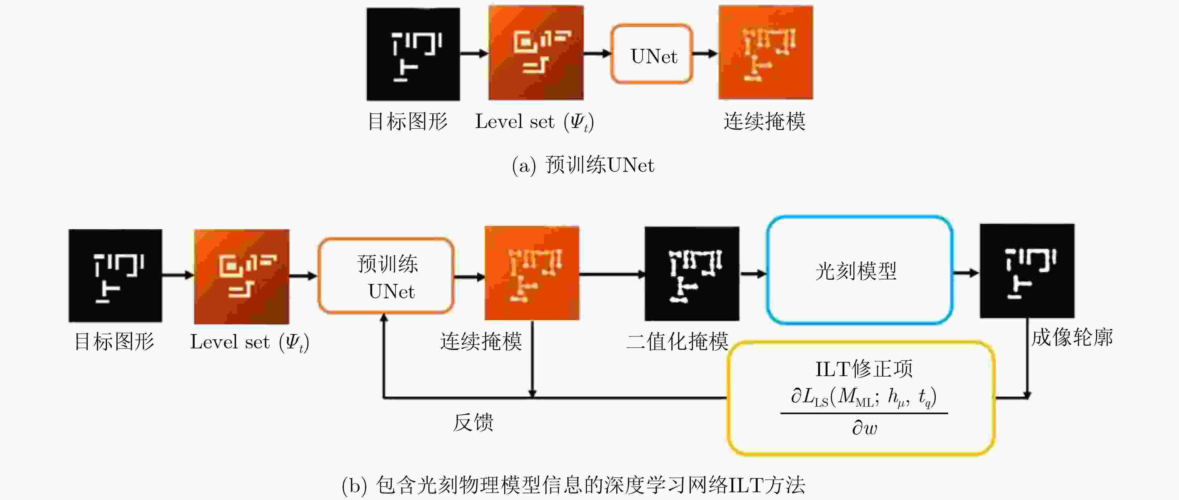
图 15 包含光刻物理模型信息的深度学习网络ILT方法流程示意图[72]
-
[1] 韦亚一, 粟雅娟, 刘艳松. 先导光刻中的光学邻近效应修正[J]. 微纳电子技术, 2014, 51(3): 186–193. doi: 10.13250/j.cnki.wndz.2014.03.009.WEI Yayi, SU Yajuan, and LIU Yansong. Optical proximity correction in the advanced photolithography[J]. Micronanoelectronic Technology, 2014, 51(3): 186–193. doi: 10.13250/j.cnki.wndz.2014.03.009. [2] LIU Yong and ZAKHOR A. Optimal binary image design for optical lithography[C]. SPIE 1264, Optical/Laser Microlithography III, San Jose, USA, 1990. doi: 10.1117/12.20216. [3] LIU Yong and ZAKHOR A. Binary and phase shifting mask design for optical lithography[J]. IEEE Transactions on Semiconductor Manufacturing, 1992, 5(2): 138–152. doi: 10.1109/66.136275. [4] ROSENBLUTH A E, BUKOFSKY S J, FONSECA C A, et al. Optimum mask and source patterns to print a given shape[J]. Journal of Micro/Nanolithography, MEMS, and MOEMS, 2002, 1(1). doi: 10.1117/1.1448500. [5] FUHNER T and ERDMANN A. Improved mask and source representations for automatic optimization of lithographic process conditions using a genetic algorithm[C]. SPIE 5754, Optical Microlithography XVIII, San Jose, USA, 2005. doi: 10.1117/12.599410. [6] PANG Linyong, SHAMMA N, RISSMAN P, et al. Laser and e-beam mask-to-silicon with inverse lithography technology (ILT)[C]. SPIE 5992, 25th Annual BACUS Symposium on Photomask Technology, Monterey, USA, 2005: 599221. doi: 10.1117/12.632738. [7] TOLANI V, PENG Danping, HE Lin, et al. Lithographic plane review (LPR) for sub-32nm mask defect disposition[C]. SPIE 7823, Photomask Technology 2010, Monterey, USA, 2010: 78232G. doi: 10.1117/12.864284. [8] SCHENKER R, BOLLEPALLI S, HU Bin, et al. Integration of pixelated phase masks for full-chip random logic layers[C]. SPIE 6924, Optical Microlithography XXI, San Jose, USA, 2008: 69240I. doi: 10.1117/12.771677. [9] TORUNOGLU I, KARAKAS A, ELSEN E, et al. OPC on a single desktop: A GPU-based OPC and verification tool for fabs and designers[C]. SPIE 7641, Design for Manufacturability through Design-Process Integration IV, San Jose, USA, 2010: 764114. doi: 10.1117/12.846636. [10] TORUNOGLU I, KARAKAS A, ELSEN E, et al. A GPU-based full-chip inverse lithography solution for random patterns[C]. SPIE 7641, Design for Manufacturability through Design-Process Integration IV, San Jose, USA, 2010: 764115. doi: 10.1117/12.846638. [11] POONAWALA A, BORODOVSKY Y, and MILANFAR P. ILT for double exposure lithography with conventional and novel materials[C]. SPIE 6520 SPIE, Optical Microlithography XX, San Jose, USA, 2007: 65202Q. doi: 10.1117/12.712382. [12] YANG Yiwei, SHI Zheng, and SHEN Shanhu. Seamless-merging-oriented parallel inverse lithography technology[J]. Journal of Semiconductors, 2009, 30(10): 106002. doi: 10.1088/1674-4926/30/10/106002. [13] ZHANG Jinyu, XIONG Wei, WANG Yan, et al. A highly efficient optimization algorithm for pixel manipulation in inverse lithography technique[C]. 2008 IEEE/ACM International Conference on Computer-Aided Design, San Jose, USA, 2008: 480–487. doi: 10.1109/ICCAD.2008.4681618. [14] ZHANG Jinyu, DENG Yangdong, XIONG Wei, et al. GPU-accelerated inverse lithography technique[C]. SPIE 7379, Photomask and Next-Generation Lithography Mask Technology XVI, Yokohama, Japan, 2009: 73790Z. doi: 10.1117/12.824276. [15] LAM E Y and WONG A K K. Computation lithography: Virtual reality and virtual virtuality[J]. Optics Express, 2009, 17(15): 12259–12268. doi: 10.1364/OE.17.012259. [16] LAM E. Regularization in inverse lithography: Enhancing manufacturability and robustness to process variations[J]. ECS Transactions, 2010, 27(1): 427–432. doi: 10.1149/1.3360655. [17] JIA Ningning and LAM E Y. Machine learning for inverse lithography: Using stochastic gradient descent for robust photomask synthesis[J]. Journal of Optics, 2010, 12(4): 045601. doi: 10.1088/2040-8978/12/4/045601. [18] SUN Shuyuan, YANG Fan, YU Bei, et al. Efficient ILT via multi-level lithography simulation[C]. 2023 60th ACM/IEEE Design Automation Conference (DAC), San Francisco, USA, 2023: 1–6. doi: 10.1109/DAC56929.2023.10247704. [19] CIOU W L, HU T, TSAI Y Y, et al. SRAF placement with generative adversarial network[C]. SPIE 11613, Optical Microlithography XXXIV, 2021: 1161305. doi: 10.1117/12.2581334. [20] XU Hui, QI Pan, TANG Fuxin, et al. SwinT-ILT: Swin transformer embedding end-to-end mask optimization model[J]. Journal of Micro/Nanopatterning, Materials, and Metrology, 2024, 23(1): 013201. doi: 10.1117/1.JMM.23.1.013201. [21] CELEPCIKAY F T, LIAO Chuncheng, HUANG T, et al. Synthesizing ILT MB-SRAF using machine learning[C]. SPIE 12954, DTCO and Computational Patterning III, San Jose, USA, 2024: 129540H. doi: 10.1117/12.3010902. [22] BORK I, BUCK P, MISHRA K, et al. Curvilinear mask process correction: Status quo and outlook[C]. SPIE 12472, 37th European Mask and Lithography Conference, Leuven, Belgium, 2022: 124720S. doi: 10.1117/12.2640001. [23] HOOKER K, XIAO Guangming, TANG Yupo, et al. Curvilinear mask solutions for full-chip EUV lithography[C]. SPIE 12054, Novel Patterning Technologies 2022, San Jose, USA, 2022: 1205407. doi: 10.1117/12.2618392. [24] PANG Linyong and FUJIMURA A. Why the mask world is moving to curvilinear[C]. SPIE 12054, DTCO and Computational Patterning III, San Jose, USA, 2024: 1295416. doi: 10.1117/12.3014640. [25] WEI Pengzhi, LI Yanqiu, LI Zhaoxuan, et al. Implicit function characterization of the curvilinear mask to realize parametric optical proximity correction with a neighborhood parallel tabu search[J]. Applied Optics, 2023, 62(18): 4848–4859. doi: 10.1364/AO.490229. [26] DIGAUM P, KAJIWARA K, KOSA N, et al. Affordable optical proximity correction runtime for EUV curvilinear mask tape-out flow[C]. SPIE 12954, DTCO and Computational Patterning III, San Jose, USA, 2024: 129540T. doi: 10.1117/12.3009981. [27] ZIMMERMANN R, ORBE L, KÜCHLER B, et al. Mask synthesis for silicon photonics devices[C].SPIE 12148, Integrated Photonics Platforms II, Strasbourg, France, 2022: 1214809. doi: 10.1117/12.2620724. [28] SHARMA R, ZUO M, BORK I, et al. A method for calibrating a curvature-based pre-bias model for advanced mask process correction applications[C]. SPIE 12293, Photomask Technology 2022, Monterey, USA, 2022: 1229309. doi: 10.1117/12.2641760. [29] XU Yan, HOU Jiechang, ZEGGAOUI N, et al. A study of ILT-based curvilinear SRAF with a constant width[C]. SPIE 12293, Photomask Technology 2022, Monterey, USA, 2022: 1229306. doi: 10.1117/12.2642989. [30] HOOKER K, XIAO Guangming, TANG Yupo, et al. Enhancing mask synthesis for curvilinear masks in full-chip extreme ultraviolet lithography[J]. Journal of Micro/Nanopatterning, Materials, and Metrology, 2023, 22(4): 041606. doi: 10.1117/1.JMM.22.4.041606. [31] LI Fu, MU Yu, FAN Jingjing, et al. Balancing mask manufacturability and image quality with inverse lithography: a study on variable fracture sizes[C]. SPIE 12953, Optical and EUV Nanolithography XXXVII, San Jose, USA, 2024: 1295310. doi: 10.1117/12.3010071. [32] KIM R H, OAK A, SHERAZI Y, et al. Manufacturing-friendly curvilinear standard cell design[C]. SPIE 12954, DTCO and Computational Patterning III, San Jose, USA, 2024: 1295405. doi: 10.1117/12.3009888. [33] SUNDARAMURTHY A. Progress in resolving mask making challenges to enable HVM curvilinear patterning[C]. SPIE PC12956, Novel Patterning Technologies 2024, San Jose, USA, 2024: PC1295608. doi: 10.1117/12.3014935. [34] CECIL T, PENG Danping, ABRAMS D, et al. Advances in inverse lithography[J]. ACS Photonics, 2023, 10(4): 910–918. doi: 10.1021/acsphotonics.2c01026. [35] WANG Jiahui, GALLAGHER E, TRIVKOVIC D, et al. EUV lithography: LER design, mask, and wafer impact[C]. SPIE 12953, Optical and EUV Nanolithography XXXVII, San Jose, USA, 2024: 129530A. doi: 10.1117/12.3011038. [36] FANG P H and YU Peichen. Tackling data inconsistency and runtime issues in inverse lithography technology (ILT) with comparative convergence study[C]. Proceedings of SPIE 12954, DTCO and Computational Patterning III, San Jose, USA, 2024: 129541E. doi: 10.1117/12.3007748. [37] 韦亚一, 粟雅娟, 董立松, 等. 计算光刻与版图优化[M]. 北京: 电子工业出版社, 2020: 107–123.WEI Yayi, SU Yajuan, DONG Lisong, et al. Computational Lithography and Layout Optimization[M]. Beijing: Publishing House of Electronics Industry, 2020: 107–123. [38] 韦亚一. 超大规模集成电路先进光刻理论与应用[M]. 北京: 科学出版, 2016: 343–368.WEI Yayi. Advanced Lithography Theory and Application of Very Large Scale Integrated Circuit[M]. Beijing: Science Press, 2016: 343–368. [39] WEI Yayi and BRAINARD R L. Advanced Processes for 193-nm Immersion Lithography[M]. Bellingham: SPIE, 2009: 336. [40] OSHER S and SETHIAN J A. Fronts propagating with curvature-dependent speed: Algorithms based on Hamilton-Jacobi formulations[J]. Journal of Computational Physics, 1988, 79(1): 12–49. doi: 10.1016/0021-9991(88)90002-2. [41] PANG Linyong, HU P, PENG Danping, et al. Source mask optimization (SMO) at full chip scale using inverse lithography technology (ILT) based on level set methods[C]. SPIE 7520, Lithography Asia 2009, Taipei, China, 2009: 75200X. doi: 10.1117/12.843578. [42] HO J, WANG Yan, WU Xin, et al. Real-world impact of inverse lithography technology[C]. SPIE 5992, 25th Annual BACUS Symposium on Photomask Technology, Monterey, USA, 2005: 59921Z. doi: 10.1117/12.632211. [43] MARTIN P M, PROGLER C J, XIAO G, et al. Manufacturability study of masks created by inverse lithography technology (ILT)[C]. SPIE 5992, 25th Annual BACUS Symposium on Photomask Technology, Monterey, USA, 2005: 599235. doi: 10.1117/12.633200. [44] LIN B, SHIEH M, SUN Jiewei, et al. Inverse lithography technology at chip scale[C]. SPIE 6154, Optical Microlithography XIX, San Jose, USA, 2006: 615414. doi: 10.1117/12.656827. [45] HUNG C Y, ZHANG Bin, GUO E, et al. Pushing the lithography limit: Applying inverse lithography technology (ILT) at the 65nm generation[C]. SPIE 6154, Optical Microlithography XIX, San Jose, USA, 2006: 61541M. doi: 10.1117/12.655728. [46] ABRAMS D S and PANG Linyong. Fast inverse lithography technology[C]. SPIE 6154, Optical Microlithography XIX, San Jose, USA, 2006: 61541J. doi: 10.1117/12.658876. [47] DAM T, TOLANI V, HU P, et al. Source-mask optimization (SMO): From theory to practice[C]. SPIE 7640, Optical Microlithography XXIII, San Jose, USA, 2010: 764028. doi: 10.1117/12.848257. [48] PANG Linyong, LIU Yong, and ABRAMS D. Inverse lithography technology (ILT): What is the impact to the photomask industry?[C]. SPIE 6283, Photomask and Next-Generation Lithography Mask Technology XIII, Yokohama, Japan, 2006: 62830X. doi: 10.1117/12.681857. [49] PANG Linyong, PENG Danping, HU P, et al. Optimization from design rules, source and mask, to full chip with a single computational lithography framework: Level-set-methods-based inverse lithography technology (ILT)[C]. SPIE SPIE 7640, Optical Microlithography XXIII, San Jose, USA, 2010: 76400O. doi: 10.1117/12.848145. [50] PANG Linyong, CECIL T, DAM T, et al. Validation of inverse lithography technology (ILT) and its adaptive SRAF at advanced technology nodes[C]. SPIE 6924, Optical Microlithography XXI, San Jose, USA, 2008: 69240T. doi: 10.1117/12.775084. [51] SINGH V, HU Bin, TOH K, et al. Making a trillion pixels dance[C]. SPIE 6924, Optical Microlithography XXI, San Jose, USA, 2008: 69240S. doi: 10.1117/12.773248. [52] PANG Linyong, RUSSELL E V, BAGGENSTOSS B, et al. Study of mask and wafer co-design that utilizes a new extreme SIMD approach to computing in memory manufacturing: Full-chip curvilinear ILT in a day[C]. Proceedings of SPIE 11148, Photomask Technology, Monterey, USA, 2019: 111480U. doi: 10.1117/12.2534629. [53] ZHENG Xianqiang, MA Xu, ZHANG Shengen, et al. Study of inverse lithography approaches based on deep learning[J]. Journal of Microelectronic Manufacturing, 2020, 3(3): 20030301. doi: 10.33079/jomm.20030301. [54] CAO Qingchen, XU Peng, SUN Song, et al. Curvilinear mask optimization with refined generative adversarial nets[J]. Journal of Micro/Nanopatterning, Materials, and Metrology, 2023, 22(1): 013201. doi: 10.1117/1.JMM.22.1.013201. [55] MOREAU M, HENRY J B, and BONNET S. A deep learning workflow to generate free-form masks for grayscale lithography[C]. SPIE 12954, DTCO and Computational Patterning III, San Jose, USA, 2024: 129540Y. doi: 10.1117/12.3009759. [56] CHIU W, HU T, HSUAN T, et al. Enhancing lithography printability through deep generative models for layout re-targeting[C]. SPIE 12954, DTCO and Computational Patterning III, San Jose, USA, 2024: 129540Q. doi: 10.1117/12.3008955. [57] ZHENG Su, YANG Haoyu, ZHU Binwu, et al. LithoBench: Benchmarking AI computational lithography for semiconductor manufacturing[C]. The 37th Conference on Neural Information Processing Systems, New Orlean, USA, 2023. [58] LAN Song, LIU Jun, WANG Yumin, et al. Deep learning assisted fast mask optimization[C]. SPIE 10587, Optical Microlithography XXXI, San Jose, USA, 2018: 105870H. doi: 10.1117/12.2297514. [59] WOLDEAMANUAL D S, ERDMANN A, and MAIER A. Application of deep learning algorithms for Lithographic mask characterization[C]. SPIE 10694, Computational Optics II, Frankfurt, Germany, 2018: 1069408. doi: 10.1117/12.2312478. [60] SIM W, LEE K, YANG Dingdong, et al. Automatic correction of lithography hotspots with a deep generative model[C]. SPIE 10961, Optical Microlithography XXXII, San Jose, USA, 2019: 1096105. doi: 10.1117/12.2514884. [61] TANABE H, JINGUJI A, and TAKAHASHI A. Evaluation of convolutional neural network for fast extreme ultraviolet lithography simulation using imec 3 nm node mask patterns[J]. Journal of Micro-Nanopatterning Materials And Metrology, 2023, 22(2): 024201. doi: 10.1117/1.JMM.22.2.024201. [62] CHEN Guojin, YU Ziyang, LIU Hongduo, et al. DevelSet: Deep neural level set for instant mask optimization[J]. IEEE Transactions on Computer-Aided Design of Integrated Circuits and Systems, 2023, 42(12): 5020–5033. doi: 10.1109/TCAD.2023.3286262. [63] CHEN Zuoxian and SHI Zheng. An efficient inverse lithography technology method based on detail-enhanced Pix2Pix network[C]. SPIE 13081, Third International Conference on Advanced Manufacturing Technology and Electronic Information (AMTEI 2023), Tianjin, China, 2024: 130810D. doi: 10.1117/12.3025959. [64] ZHU Binwu, ZHENG Su, YU Ziyang, et al. L2O-ILT: Learning to optimize inverse lithography techniques[J]. IEEE Transactions on Computer-Aided Design of Integrated Circuits and Systems, 2024, 43(3): 944–955. doi: 10.1109/TCAD.2023.3323164. [65] AKKIRAJU N and TORUNOGLU I. A machine learning approach to inverse lithography[C]. SPIE 12052, DTCO and Computational Patterning, San Jose, USA, 2022: 120520W. doi: 10.1117/12.2613163. [66] MA Xu, ZHAO Qile, ZHANG Hao, et al. Model-driven convolution neural network for inverse lithography[J]. Optics Express, 2018, 26(25): 32565–32584. doi: 10.1364/OE.26.032565. [67] YUAN Pengpeng, XU Peng, and WEI Yayi. Optical proximity correction with the conditional Wasserstein GAN[C]. SPIE 12495, DTCO and Computational Patterning II, San Jose, USA, 2023: 124951F. doi: 10.1117/12.2657584. [68] CAO Qingchen, XU Peng, WEI Juan, et al. Hybrid deep learning OPC framework with generative adversarial network[C]. SPIE 12495, DTCO and Computational Patterning II, San Jose, USA, 2023: 124951R. doi: 10.1117/12.2658271. [69] CIOU Weilun, HU T, TSAI Yiyen, et al. Machine learning optical proximity correction with generative adversarial networks[J]. Journal of Micro/Nanopatterning, Materials, and Metrology, 2022, 21(4): 041606. doi: 10.1117/1.JMM.21.4.041606. [70] CAO Qingchen, XU Peng, SUN Song, et al. Generation of inverse assist features using generative adversarial networks[J]. Microelectronic Engineering, 2023, 273: 111951. doi: 10.1016/j.mee.2023.111951. [71] ZHANG Shengen, MA Xu, and ZHANG Junbi. Fast inverse lithography approach based on a model-driven graph convolutional network[J]. Optics Express, 2023, 31(22): 36451–36467. doi: 10.1364/OE.493178. [72] MA Xingyu and HAO Shaogang. Inverse lithography physics-informed deep neural level set for mask optimization[J]. Applied Optics, 2023, 62(33): 8769–8779. doi: 10.1364/AO.503332. [73] HUNG C Y, ZHANG Bin, TANG Deming, et al. First 65nm tape-out using inverse lithography technology (ILT)[C]. SPIE 5992, 25th Annual BACUS Symposium on Photomask Technology, Monterey, California, USA, 2005: 59921U. doi: 10.1117/12.632415. [74] CECIL T, BRAAM K, OMRAN A, et al. Establishing fast, practical, full-chip ILT flows using machine learning[C]. SPIE 11327, Optical Microlithography XXXIII, San Jose, USA, 2020: 1132706. doi: 10.1117/12.2551425. [75] SHI Xuelong, YAN Yan, ZHOU Tao, et al. Fast and accurate machine learning inverse lithography using physics based feature maps and specially designed DCNN[C]. 2020 International Workshop on Advanced Patterning Solutions (IWAPS), Chengdu, China, 2020: 1–3. doi: 10.1109/IWAPS51164.2020.9286814. [76] SUN Yiyu, LI Yanqiu, and LIU Lihui. Inverse lithography source and mask optimization via Bayesian compressive sensing[J]. Applied Optics, 2022, 61(20): 5838–5843. doi: 10.1364/AO.461288. -


 下载:
下载:






 下载:
下载:
