




Radiation-Hardened Ga2O3 MOSFET Design Featuring NiO Heterojunction and Comb-Shaped Gate Modulation
-
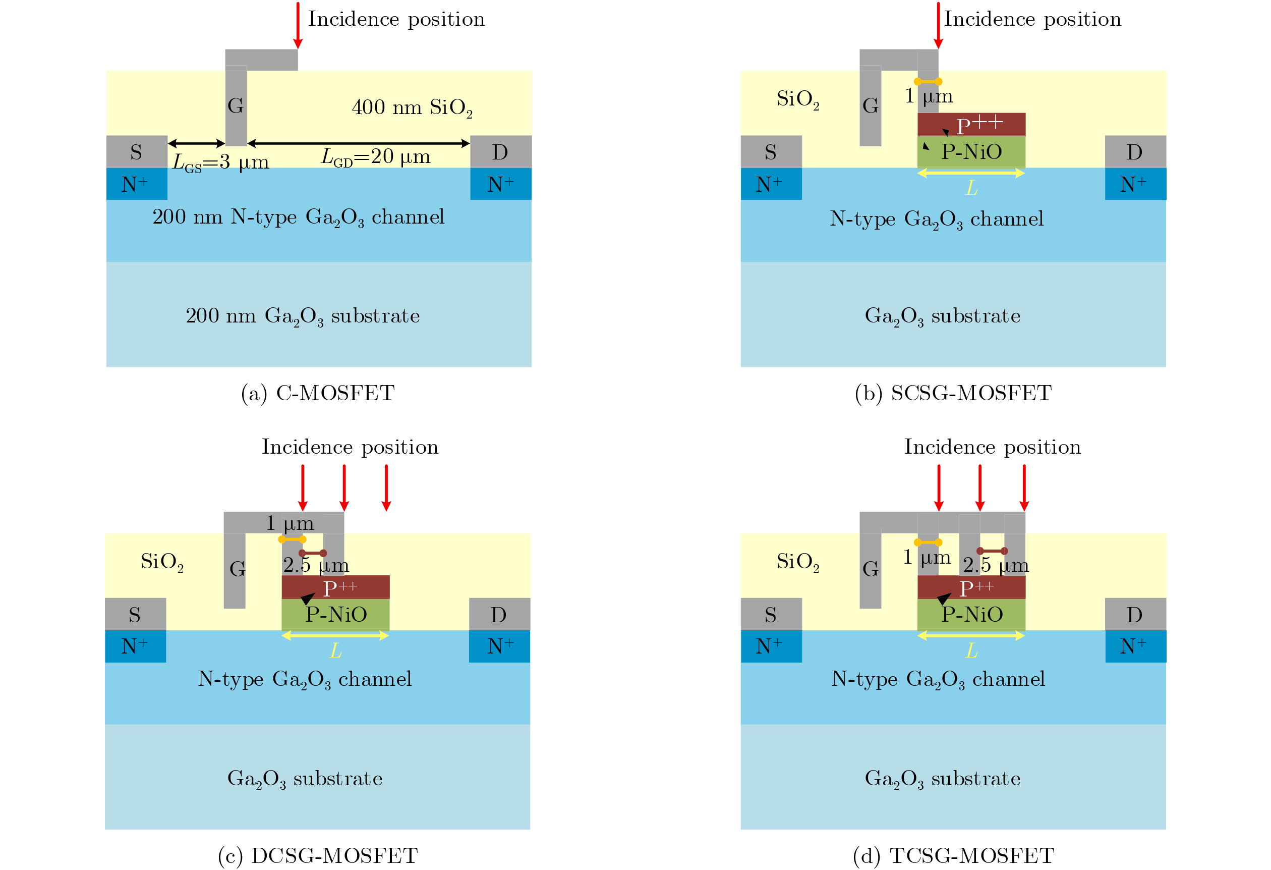
摘要: 该文提出一种具备抗单粒子烧毁(SEB)能力的复合叉指栅柱结构氧化镓金属氧化物半导体场效应晶体管(CSG-MOSFET)。该器件在N型Ga2O3沟道层上方引入P型NiO层,并通过叉指栅柱将其与延伸栅场板实现电气连接。基于P-NiO/N-Ga2O3异质结的电荷补偿效应,该结构显著优化了沟道内的电场分布。同时,叉指栅柱作为关键的电场调制单元,与延伸场板协同作用,不仅有效抑制了传统器件(C-MOSFET)中栅极场板边缘的电场拥挤效应,更将易诱发单粒子雪崩击穿的峰值电场区域从脆弱的栅极边缘主动转移至最外侧栅柱边缘。TCAD仿真结果表明,在重离子辐照下,所提CSG-MOSFET将其SEB阈值电压(VSEB)从传统器件的240 V大幅提升至
2280 V,充分证实了该复合结构在提升Ga2O3功率器件抗辐射性能方面的优势。-
关键词:
- Ga2O3 MOSFET /
- 抗辐照加固 /
- 叉指栅柱
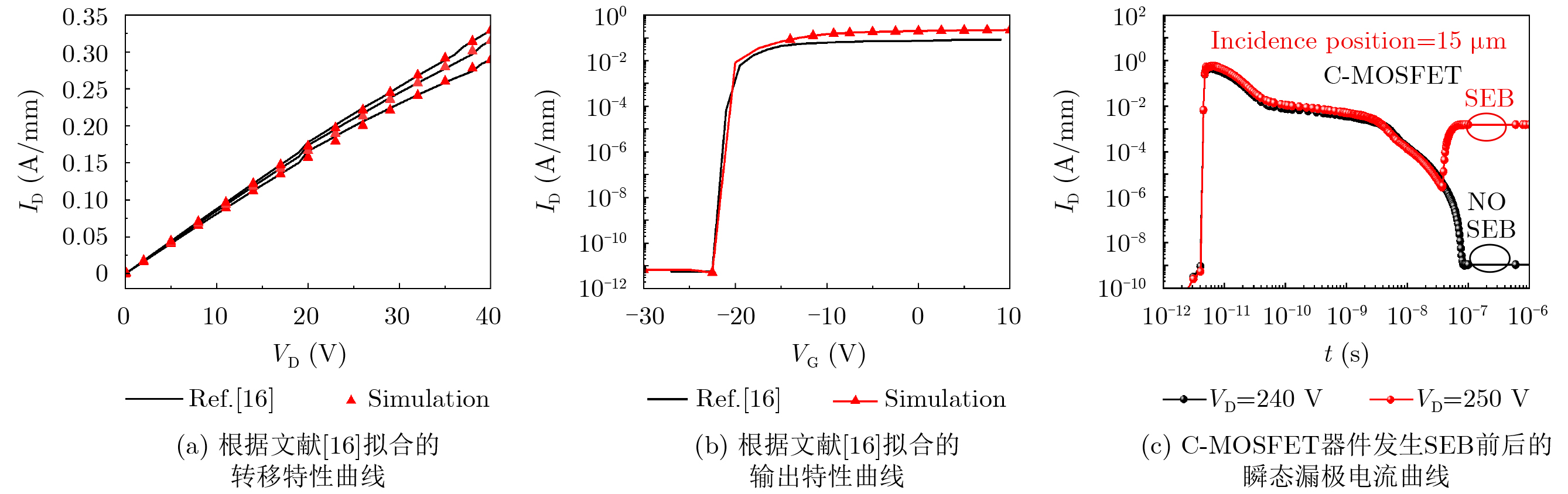
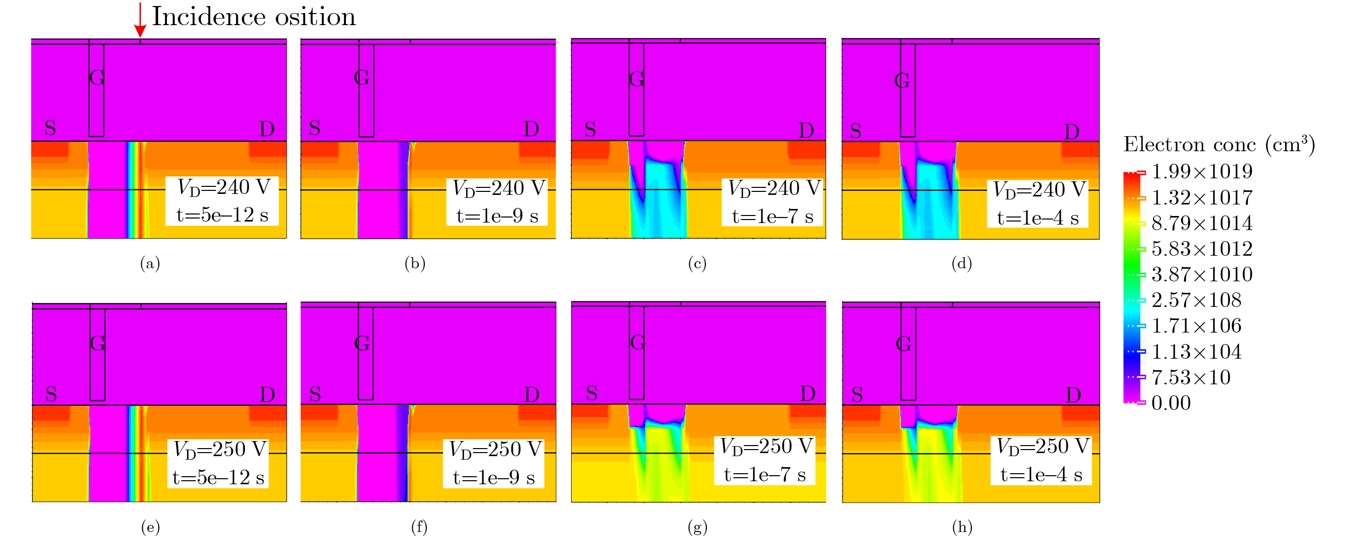
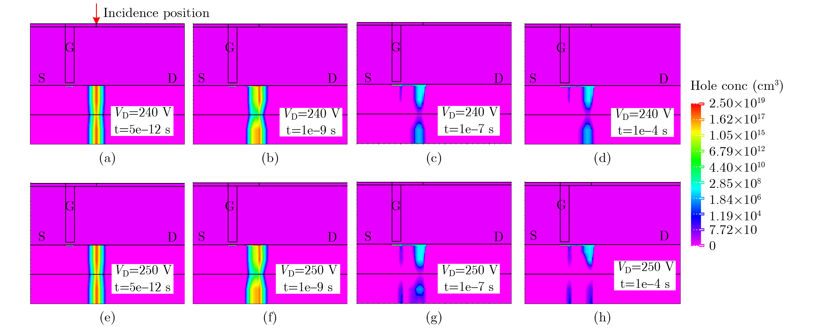
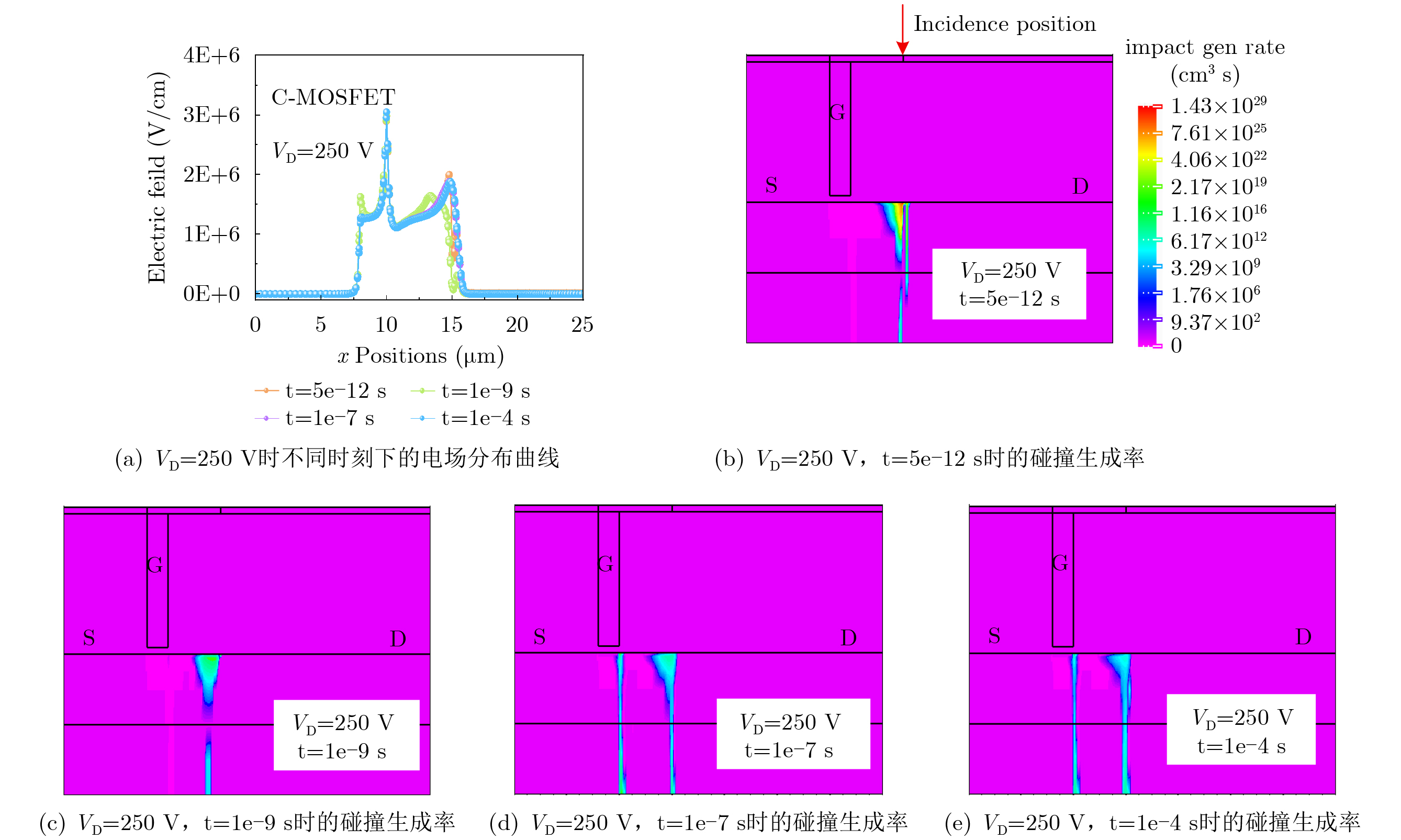
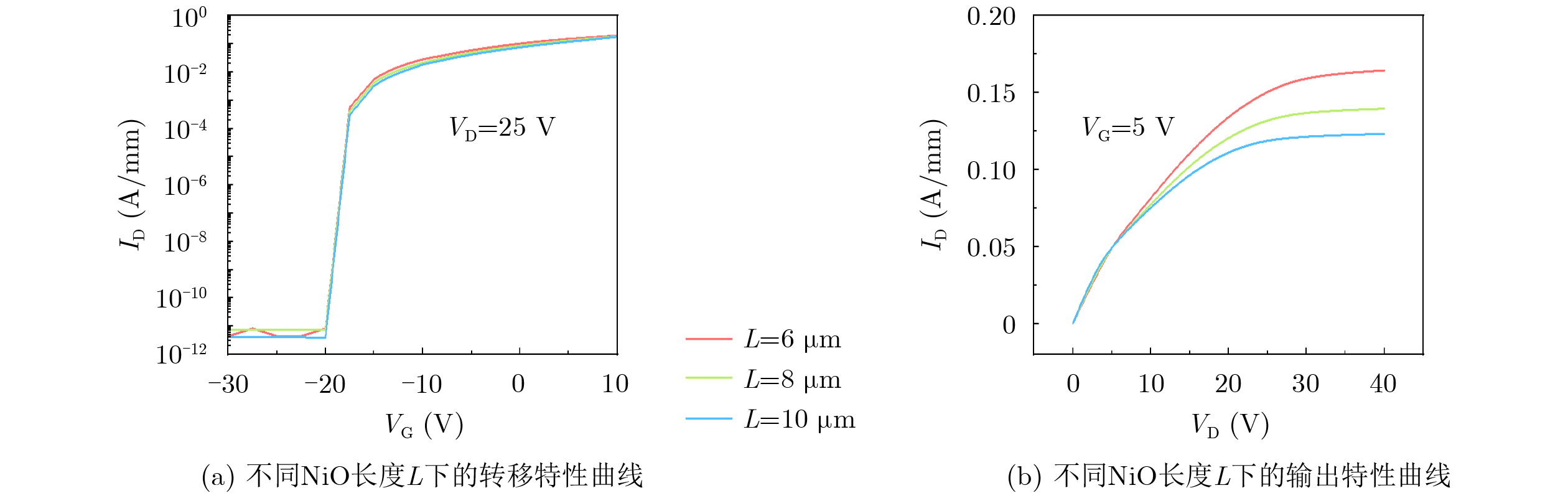
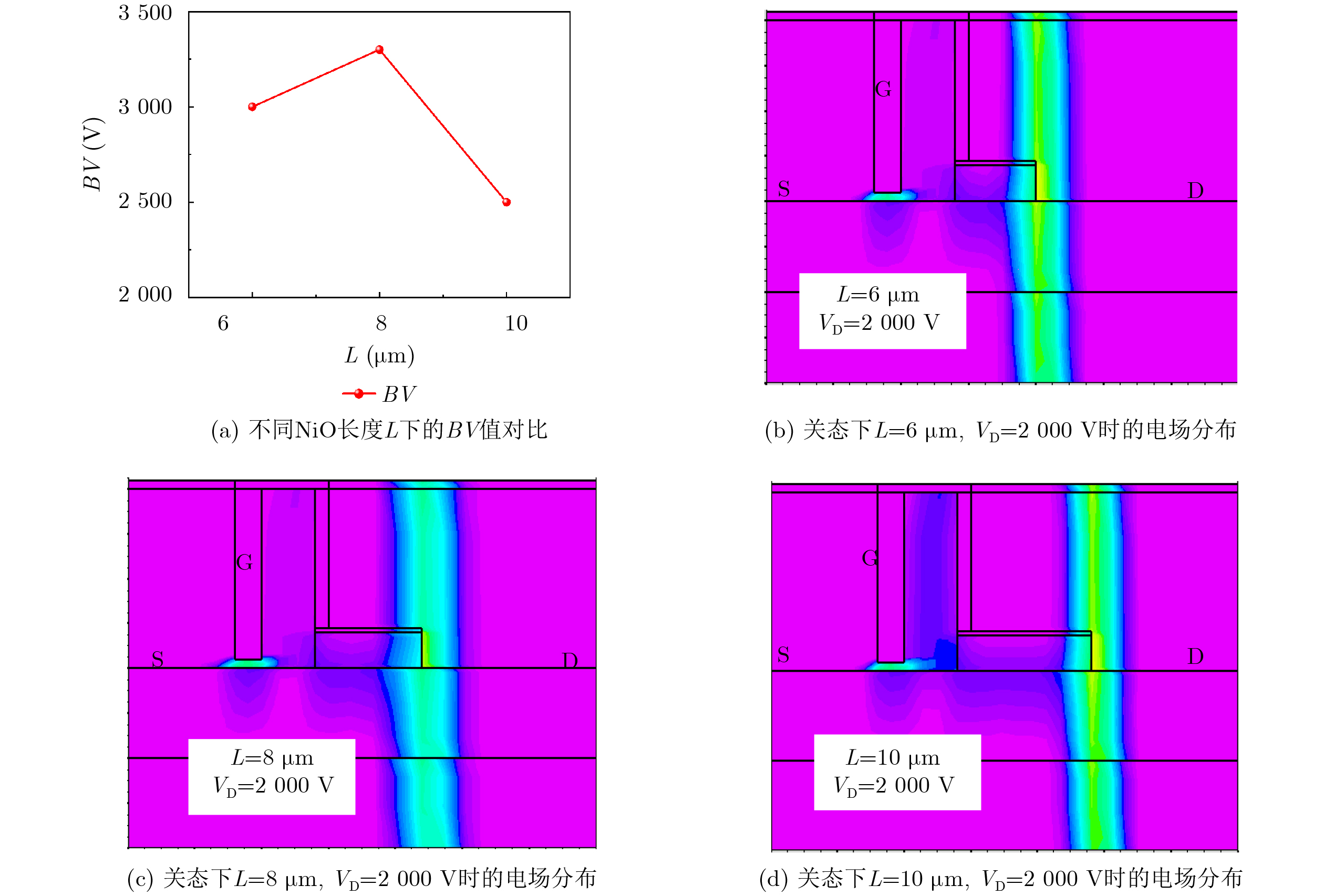
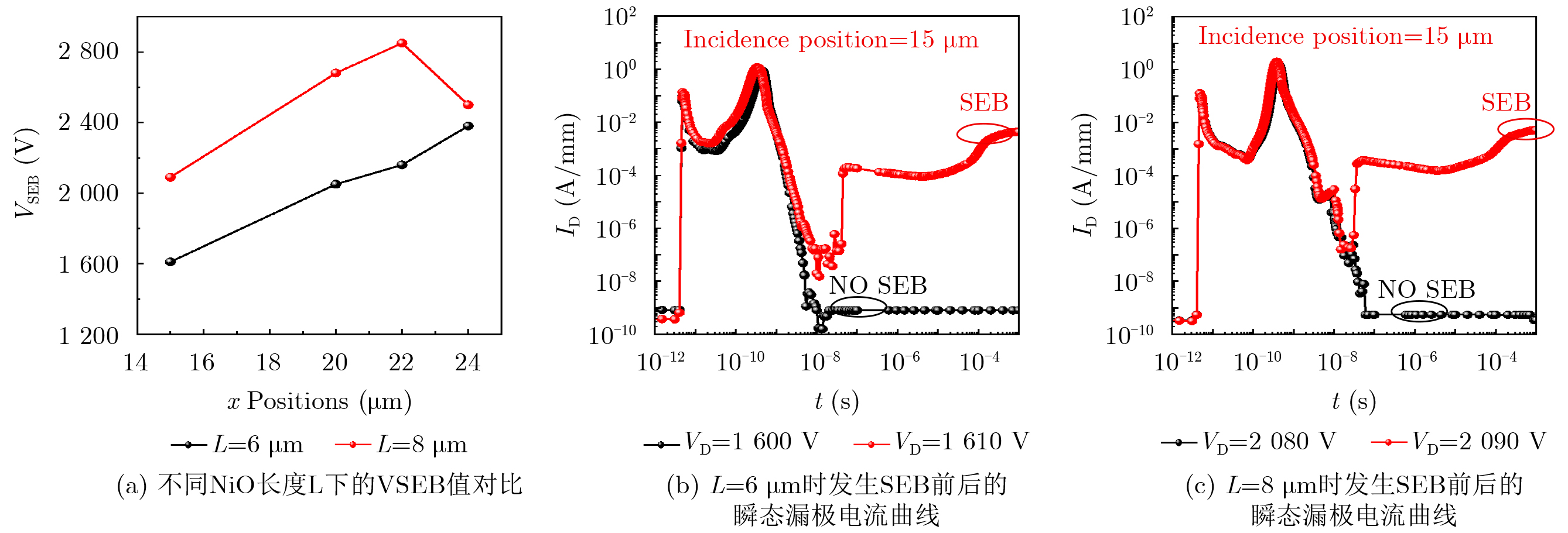
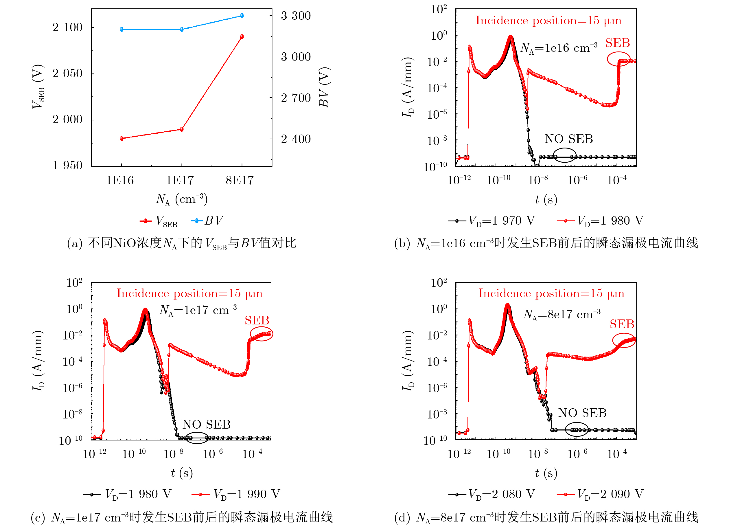
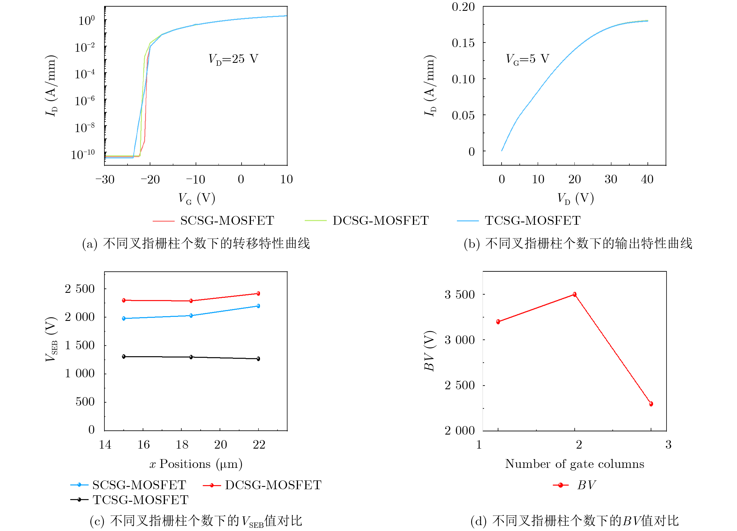
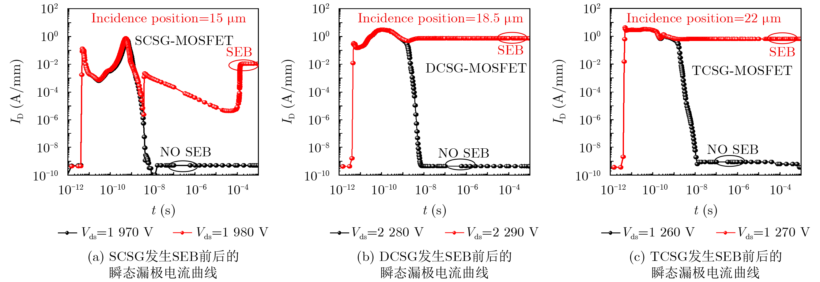
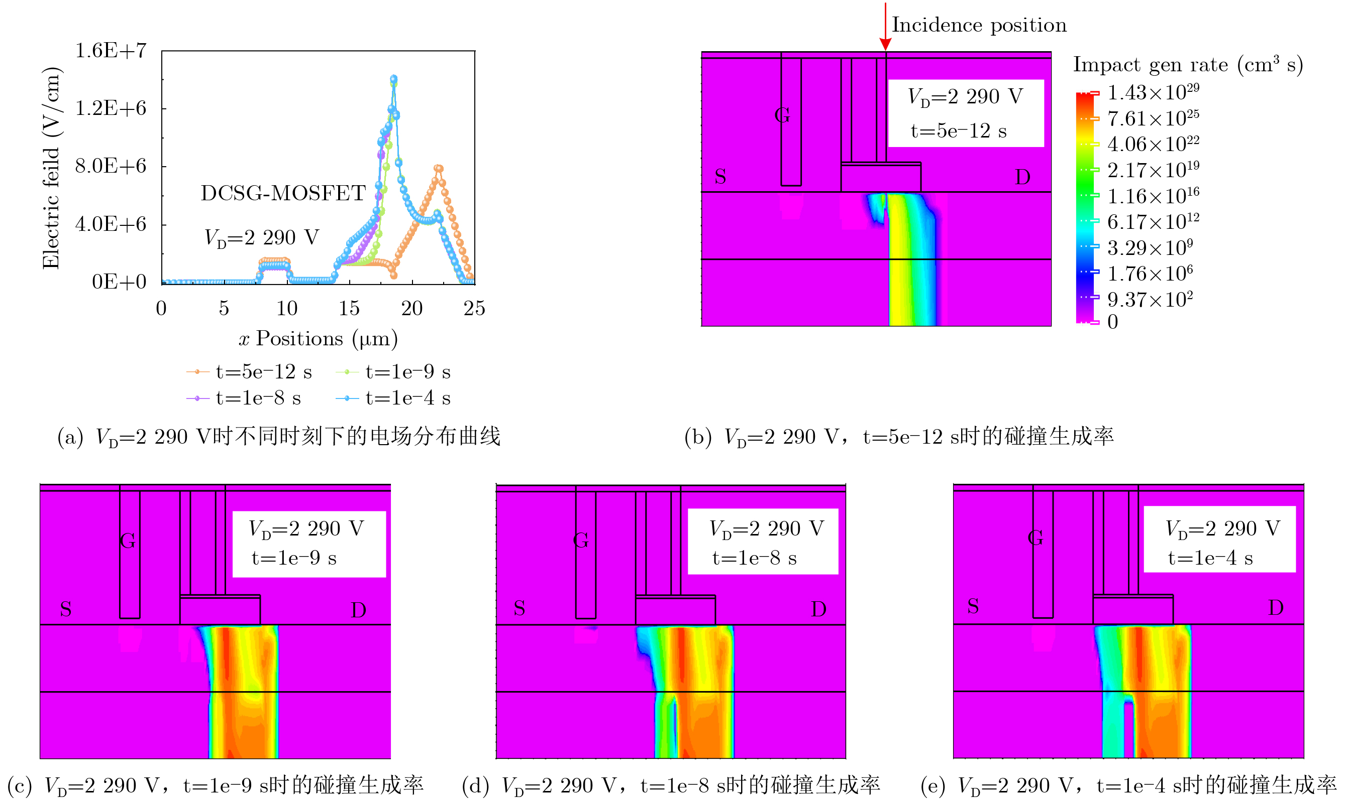
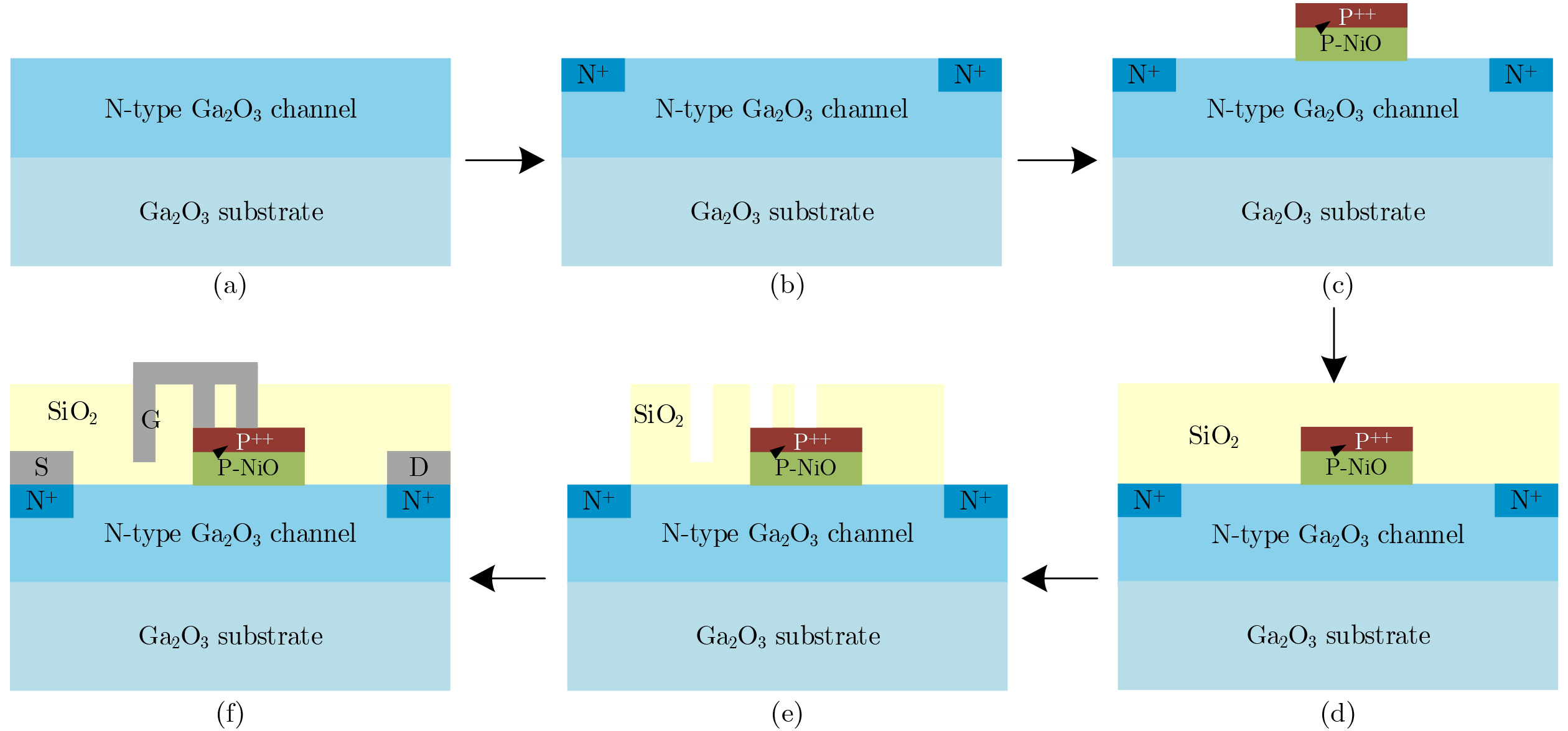
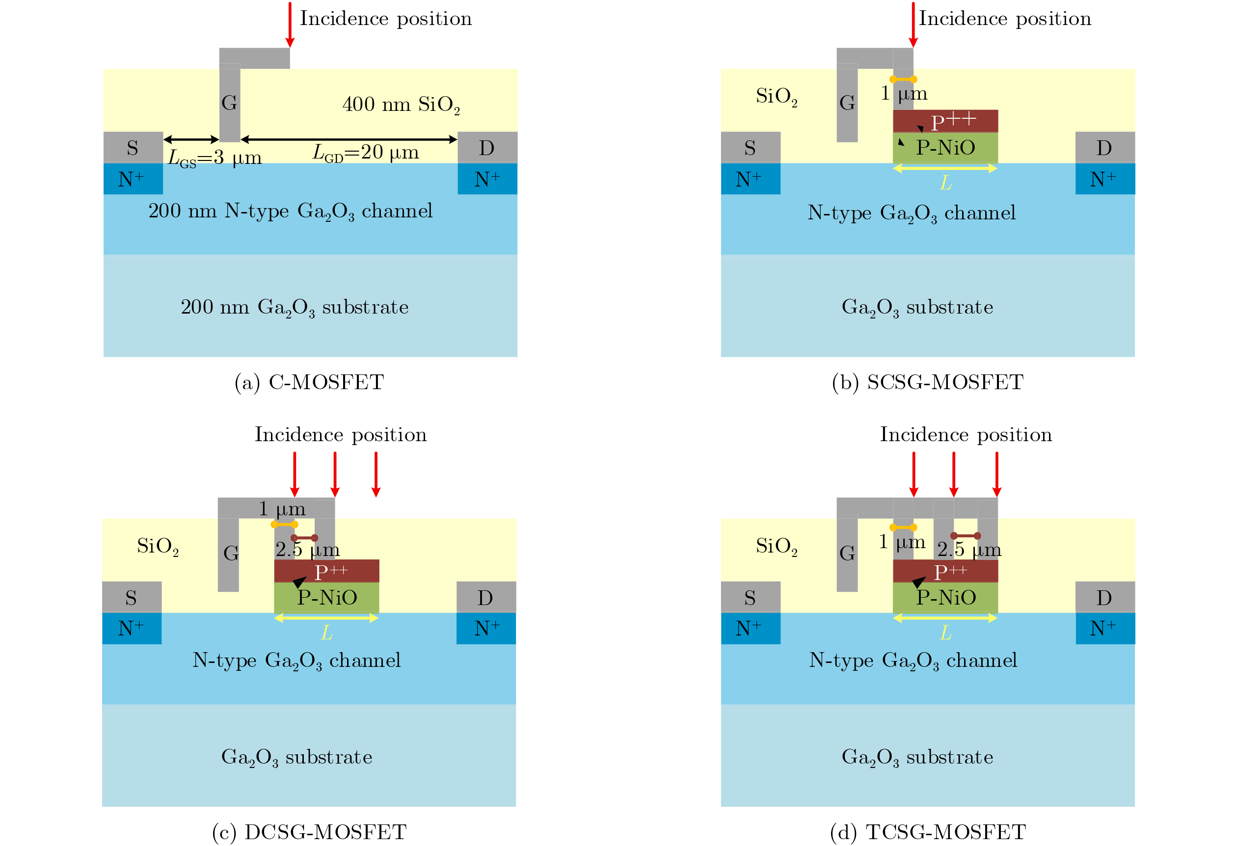
Abstract:Objective Gallium Oxide Metal-Oxide-Semiconductor Field-Effect Transistor (Ga2O3 MOSFET) is regarded as a promising power device for high-voltage applications, particularly in aerospace and satellite power systems, because of its ultra-wide bandgap and high critical breakdown field. However, the Conventional MOSFET (C-MOSFET) exhibits limited reliability in space radiation environments. Under off-state conditions, the electric field is highly concentrated near the gate edge. Heavy-ion irradiation generates dense electron-hole pairs along the ion track. Driven by the intense electric field, these carriers undergo avalanche multiplication through impact ionization, causing the drain current to increase sharply without recovery and ultimately leading to irreversible Single-Event Burnout (SEB) at relatively low drain bias. This failure mechanism severely limits the application of Ga2O3 MOSFETs in harsh radiation environments. Furthermore, the lack of reliable and efficient p-type doping restricts the implementation of conventional radiation-hardening techniques, including junction termination extension and junction isolation. Therefore, ionization-induced carriers readily accumulate in sensitive regions, increasing susceptibility to Single-Event Effect (SEE). The extremely low thermal conductivity of Ga2O3 further promotes local heat accumulation following heavy-ion irradiation, producing localized hot spots that increase the likelihood of thermal burnout. Existing hardening approaches, including field-plate optimization and dielectric engineering, provide only limited improvement. Moreover, the application of heterojunction structures for radiation hardening has rarely been investigated, and systematic hardening strategies have not yet been established. To address these limitations, this paper proposes a Comb-Shaped Gate Metal-Oxide-Semiconductor Field-Effect Transistor (CSG-MOSFET) incorporating a NiO heterojunction. The proposed structure redistributes the channel electric field, suppresses electric-field crowding at the conventional gate edge, and significantly improves SEB tolerance, providing an effective solution for Ga2O3 power devices operating in harsh radiation environments. Methods Technology Computer-Aided Design (TCAD) simulations are performed to evaluate the electrical characteristics and SEB performance of the proposed CSG-MOSFET in comparison with the C-MOSFET. The simulations incorporate high-field mobility, Shockley-Read-Hall recombination, Auger recombination, impact ionization, and heavy-ion models. Based on the charge-compensation effect of the p-NiO/n-Ga2O3 heterojunction, the proposed structure utilizes the extended depletion region formed at the heterointerface to redistribute the channel electric field. This heterojunction-induced depletion region improves electric-field uniformity and enhances SEB tolerance. Furthermore, the comb-shaped gate columns, operating together with the extended gate field plate, relocate the peak electric field away from the conventional gate edge, suppress local electric-field crowding, and improve device reliability under high-voltage and radiation conditions. Results and Discussions Simulation results demonstrate that the optimized Double Comb-Shaped Gate MOSFET (DCSG-MOSFET) significantly improves radiation hardness compared with the C-MOSFET. The SEB Threshold Voltage (VSEB) increases from 240 V to 2 280 V, while the Breakdown Voltage (BV) increases from 2 000 V to 3 500 V. Meanwhile, the specific on-resistance decreases. Therefore, the Baliga Figure of Merit (BFOM) and the SEB-based figure of merit are substantially improved. The NiO heterojunction and comb-shaped gate columns effectively redistribute the electric field, shifting the peak electric field from the conventional gate edge to the outer gate-column edge and suppressing local electric-field crowding. These improvements substantially enhance the radiation hardness of the device. Conclusions A radiation-hardened DCSG-MOSFET incorporating a NiO heterojunction is proposed and evaluated using TCAD simulations. The optimized structure significantly improves SEB tolerance while maintaining excellent electrical performance. Compared with the C-MOSFET, both VSEB and BV are substantially increased, demonstrating enhanced blocking capability. Charge compensation at the p-NiO/n-Ga2O3 heterojunction forms an extended depletion region that effectively redistributes the channel electric field and suppresses electric-field crowding near the conventional gate edge. Furthermore, the comb-shaped gate columns, operating together with the extended gate field plate, relocate the peak electric field to the outermost gate-column edge, thereby suppressing impact ionization induced by heavy-ion irradiation and effectively mitigating SEB. The reduced specific on-resistance further improves the BFOM and the SEB-based figure of merit. These results demonstrate that the proposed DCSG-MOSFET is a promising candidate for power electronic applications in harsh radiation environments, including aerospace and satellite systems. -
表 1 所有器件的主要参数
器件参数 数值 N型Ga2O3沟道掺杂浓度 5×1017 cm–3 N+区掺杂浓度 1×1019 cm–3 N+区厚度 50 nm P-NiO区厚度 80 nm P-NiO区长度 (L) 变量 P-NiO区掺杂浓度(NA) 变量 P++区厚度 10 nm P++区掺杂浓度 1×1019 cm–3  下载: 导出CSV
表 2 所有器件的主要电学特性参数(L=8 μm, NA=1e16 cm–3)
器件特性 C-MOSFET SCSG-MOSFET DCSG-MOSFET TCSG-MOSFET Vth(V) –20 –20 –20 –20 Ron,sp(mΩ/cm2) 39.6 31.4 31.4 31.4 BV(V) 2000 3200 3500 2300 VSEB(V) 240 1970 2280 1260 BFOM(BV2/Ron,sp) 0.1 GW/cm2 0.33 GW/cm2 0.39 GW/cm2 0.17 GW/cm2 BFOM(VSEB2/Ron,sp) 0.001 GW/cm2 0.12 GW/cm2 0.17 GW/cm2 0.05 GW/cm2
下载: 导出CSV
-
[1] ATMACA G and CHA H Y. Normally-off recessed gate β-Ga2O3 MOSHFETs with a modulation-doped heterostructure back-barrier[J]. Physica Scripta, 2024, 99(3): 035901. doi: 10.1088/1402-4896/ad213f. [2] HASAN A S M K, HOSSAIN M M, HERIS P C, et al. Single event upset in depletion-mode gallium oxide MOSFETs at the breakdown region[C]. 2024 IEEE Applied Power Electronics Conference and Exposition (APEC), Long Beach, USA, 2024: 2461–2467. doi: 10.1109/APEC48139.2024.10509030. [3] WONG M H, TAKEYAMA A, MAKINO T, et al. Radiation hardness of β-Ga2O3 metal-oxide-semiconductor field-effect transistors against gamma-ray irradiation[J]. Applied Physics Letters, 2018, 112(2): 023503. doi: 10.1063/1.5017810. [4] WANG Kejia, WANG Zujun, CAO Rongxin, et al. Study of the mechanism of single event burnout in lateral depletion-mode Ga2O3 MOSFET devices via TCAD simulation[J]. Journal of Applied Physics, 2024, 135(14): 145702. doi: 10.1063/5.0184704. [5] KONG Moufu, YANG Mingliang, DENG Hongfei, et al. A novel lateral superjunction Ga2O3 MOSFET with a self-biased accumulation layer for ultra-low specific on-resistance and improved FOM[J]. Semiconductor Science and Technology, 2025, 40(4): 045009. doi: 10.1088/1361-6641/adc1fd. [6] GOYAL P and KAUR H. Implementing variable doping and work function engineering in β-Ga2O3 MOSFET to realize high breakdown voltage and PfoM[J]. Semiconductor Science and Technology, 2022, 37(4): 045018. doi: 10.1088/1361-6641/ac5843. [7] WANG Chenlu, YAN Qinglong, SU Chunxu, et al. Demonstration of the β-Ga2O3 MOS-JFETs with suppressed gate leakage current and large gate swing[J]. IEEE Electron Device Letters, 2023, 44(3): 380–383. doi: 10.1109/LED.2023.3237598. [8] YOU Jinle, LIAO Fei, MA Zepeng, et al. High-performance lateral enhancement-mode β-Ga2O3 MOSFET with a novel superjunction-extended gate structure[J]. Semiconductor Science and Technology, 2025, 40(8): 085004. doi: 10.1088/1361-6641/adf661. [9] MA Hongye, WANG Wentao, CAI Yuncong, et al. Analysis of single event effects by heavy ion irradiation of Ga2O3 metal-oxide-semiconductor field-effect transistors[J]. Journal of Applied Physics, 2023, 133(8): 085701. doi: 10.1063/5.0107325. [10] WANG Zefeng, LIU Fengkai, LIU Zhongli, et al. Simulation of the single-event burnout in lateral enhancement-mode β-Ga2O3 MOSFET devices[J]. IEEE Transactions on Device and Materials Reliability, 2026, 26(1): 351–357. doi: 10.1109/TDMR.2026.3658196. [11] YU Chenghao, GUO Haomin, LIU Yan, et al. Simulation study on single-event burnout in field-plated Ga2O3 MOSFETs[J]. Microelectronics Reliability, 2023, 149: 115227. doi: 10.1016/j.microrel.2023.115227. [12] LEI Weina, DANG Kui, ZHOU Hong, et al. Proposal and simulation of Ga2O3 MOSFET with PN heterojunction structure for high-performance E-mode operation[J]. IEEE Transactions on Electron Devices, 2022, 69(7): 3617–3622. doi: 10.1109/TED.2022.3172919. [13] HUANG Jiaweiwen, CHEN Wensuo, ZHAO Shenglei, et al. High performance E-mode NiO/β-Ga2O3 HJ-FET with high conduction band offset and thin recessed channel[J]. Micro and Nanostructures, 2024, 195: 207963. doi: 10.1016/j.micrna.2024.207963. [14] MIAO Ruixia, JI Xiang, WANG Jiaqi, et al. Single event effect of E-mode Ga2O3 heterojunction field effect transistor under heavy ion irradiation[C]. 2025 4th International Symposium on Semiconductor and Electronic Technology (ISSET), Xi’an, China, 2025: 633–638. doi: 10.1109/ISSET66828.2025.11185020. [15] WANG Wentao, CAI Yuncong, TIAN Xusheng, et al. Simulation research on high-voltage β-Ga2O3 MOSFET based on floating field plate[J]. ECS Journal of Solid State Science and Technology, 2024, 13(2): 025002. doi: 10.1149/2162-8777/ad28c9. [16] DATTA A and SINGISETTI U. Simulation studies of single-event effects in β-Ga2O3 MOSFETs[J]. IEEE Transactions on Electron Devices, 2024, 71(1): 476–483. doi: 10.1109/TED.2023.3330132. [17] HAN Yixin, LUO Zixiang, WANG Jialin, et al. Simulation research on a Ga2O3-based superjunction field effect transistor[J]. ECS Journal of Solid State Science and Technology, 2025, 14(7): 075002. doi: 10.1149/2162-8777/adeae4. -

 下载:
下载:

图(17) / 表(2)
计量
- 文章访问数: 767
- HTML全文浏览量: 311
- PDF下载量: 35
- 被引次数: 0
