Advanced Search
Turn off MathJax
Article Contents
GAO Sheng, ZHANG Lin, WU Yanjun, WANG Qi, JING Liang. Radiation-Hardened Ga2O3 MOSFET Design Featuring NiO Heterojunction and Comb-Shaped Gate Modulation[J]. Journal of Electronics & Information Technology. doi: 10.11999/JEIT260396
Citation: GAO Sheng, ZHANG Lin, WU Yanjun, WANG Qi, JING Liang. Radiation-Hardened Ga2O3 MOSFET Design Featuring NiO Heterojunction and Comb-Shaped Gate Modulation[J]. Journal of Electronics & Information Technology. doi: 10.11999/JEIT260396

Radiation-Hardened Ga2O3 MOSFET Design Featuring NiO Heterojunction and Comb-Shaped Gate Modulation

doi: 10.11999/JEIT260396 cstr: 32379.14.JEIT260396
Funds:  The National Natural Science Foundation of China (62404026)
  • Accepted Date: 2026-07-03
  • Rev Recd Date: 2026-07-03
  • Available Online: 2026-07-12
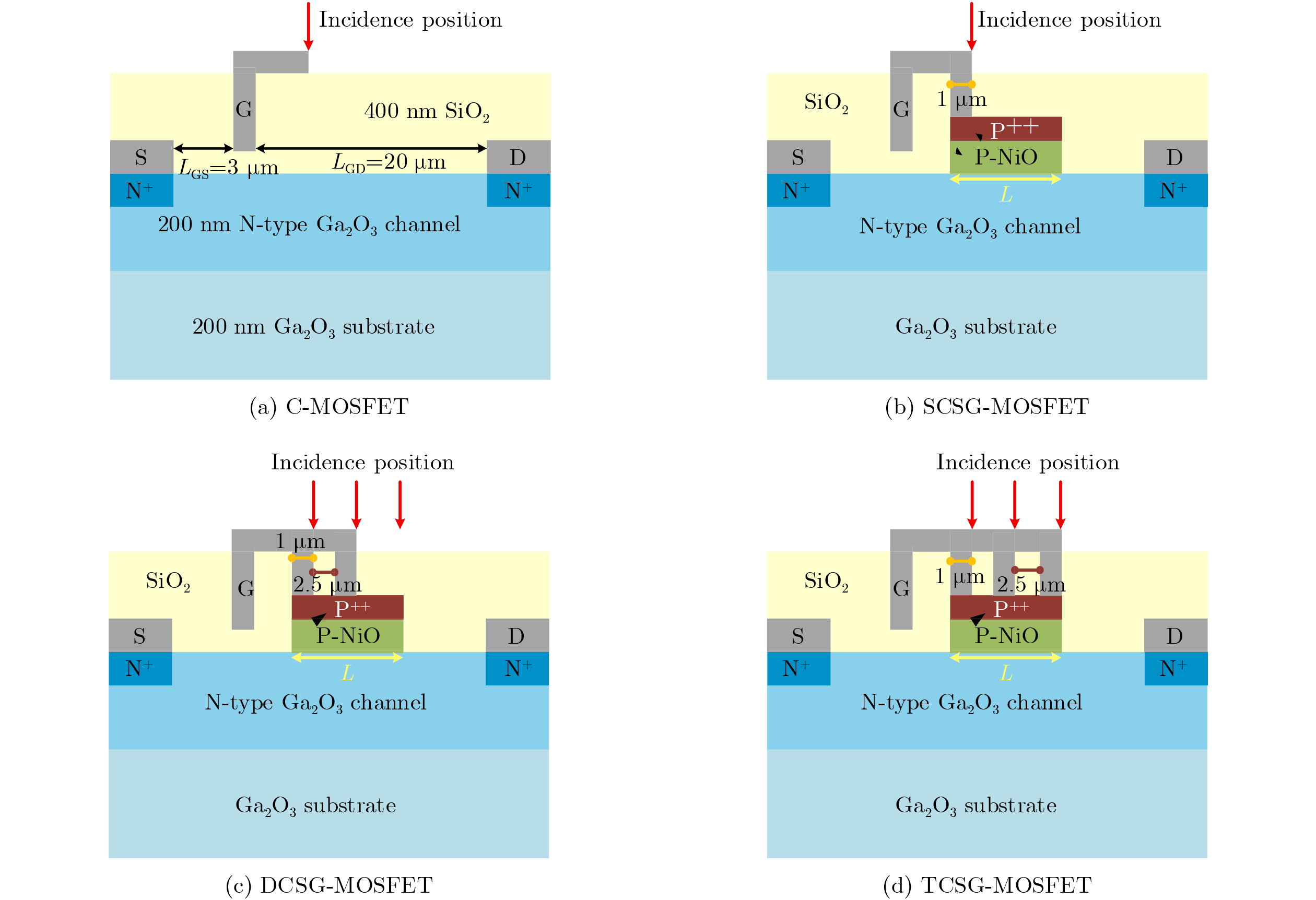
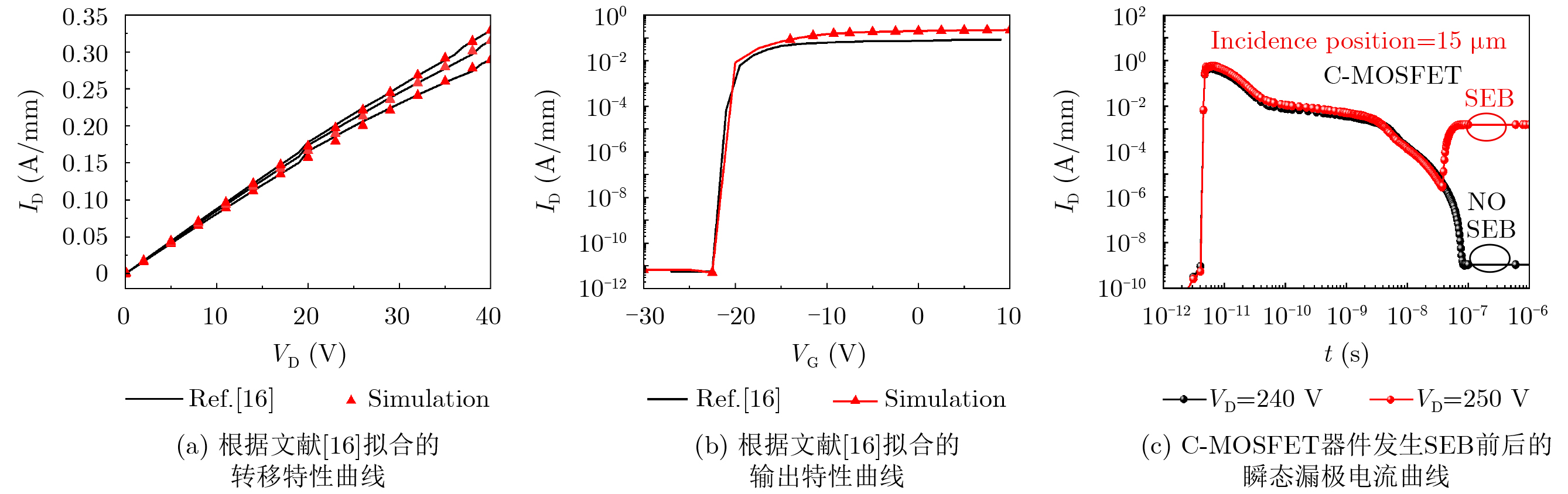
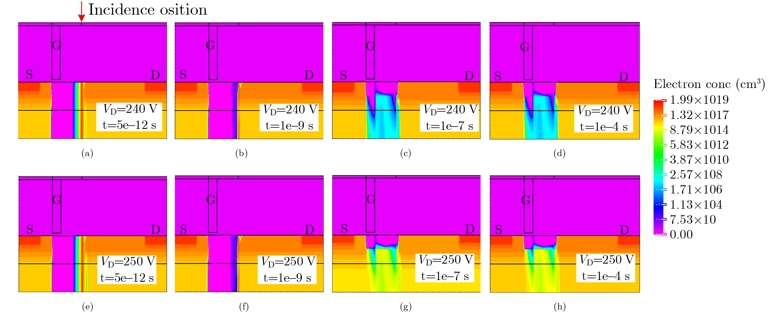
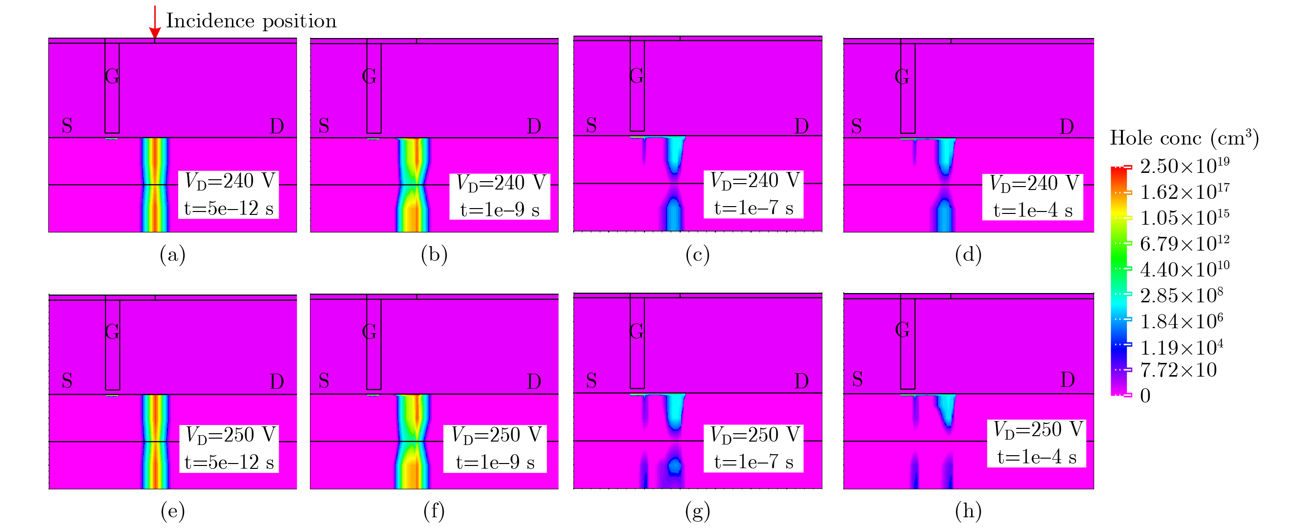
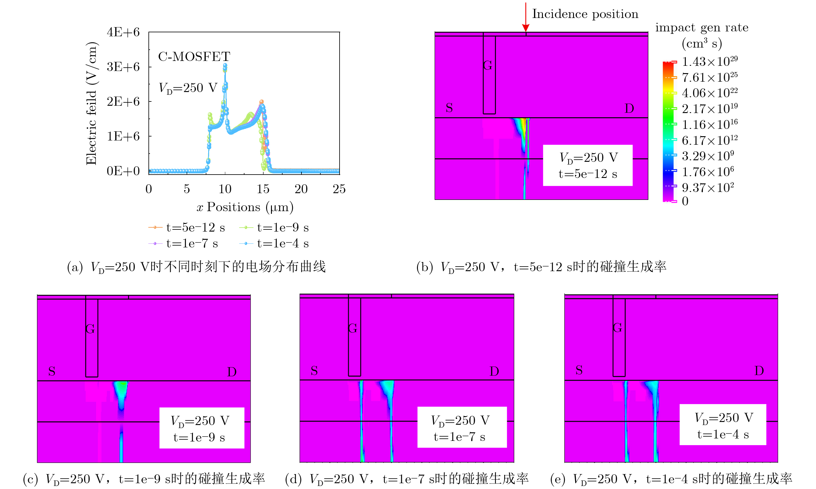
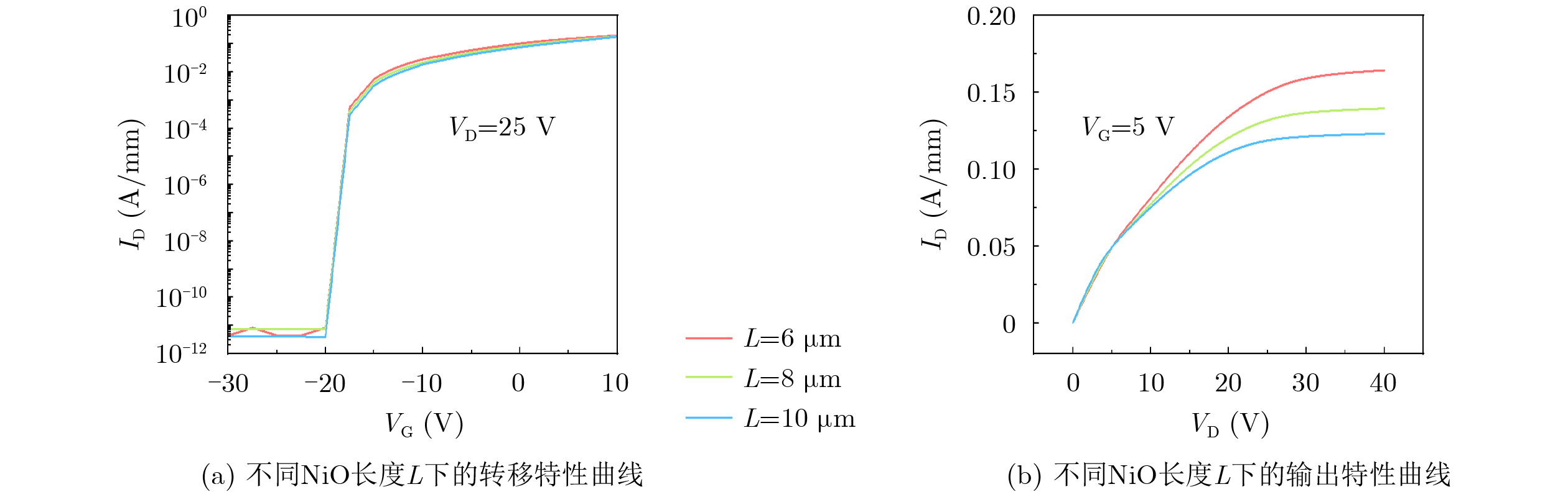
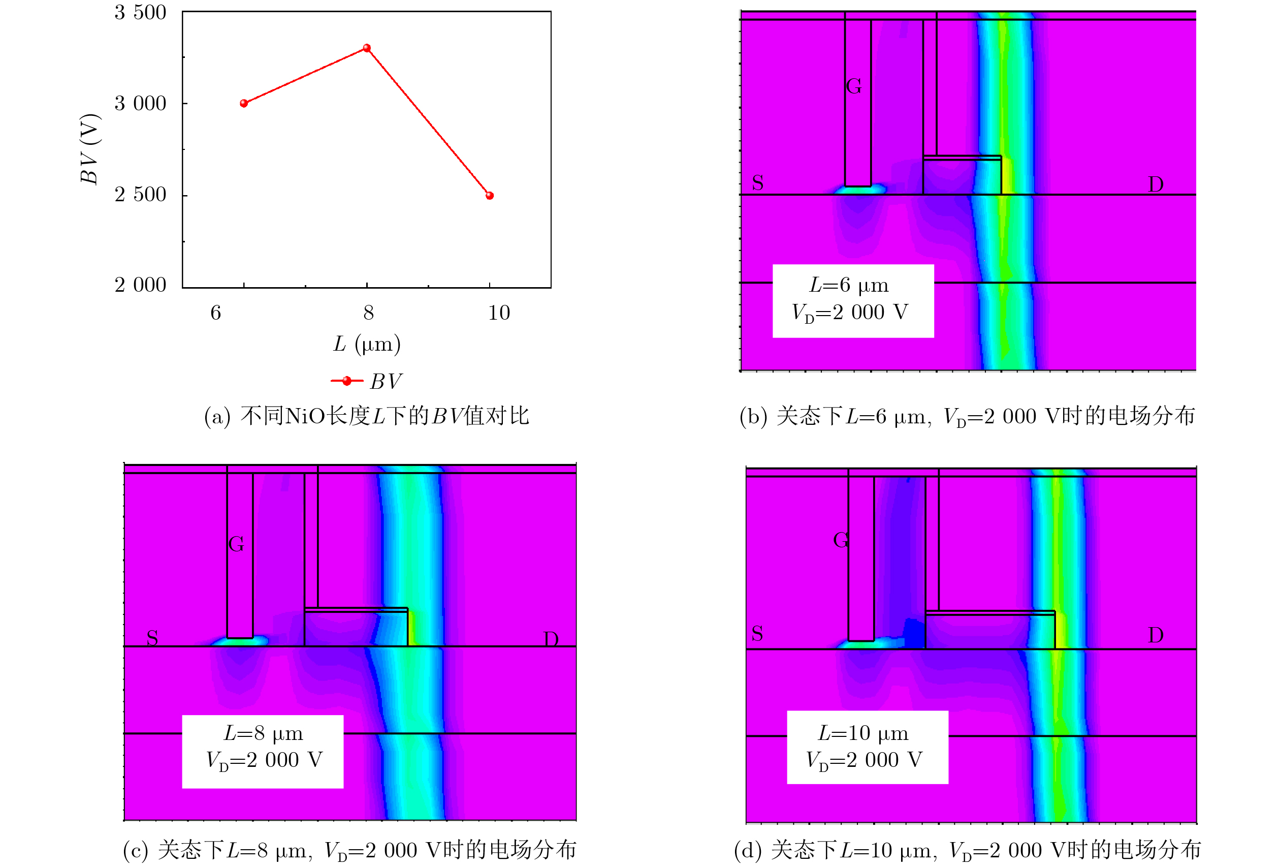
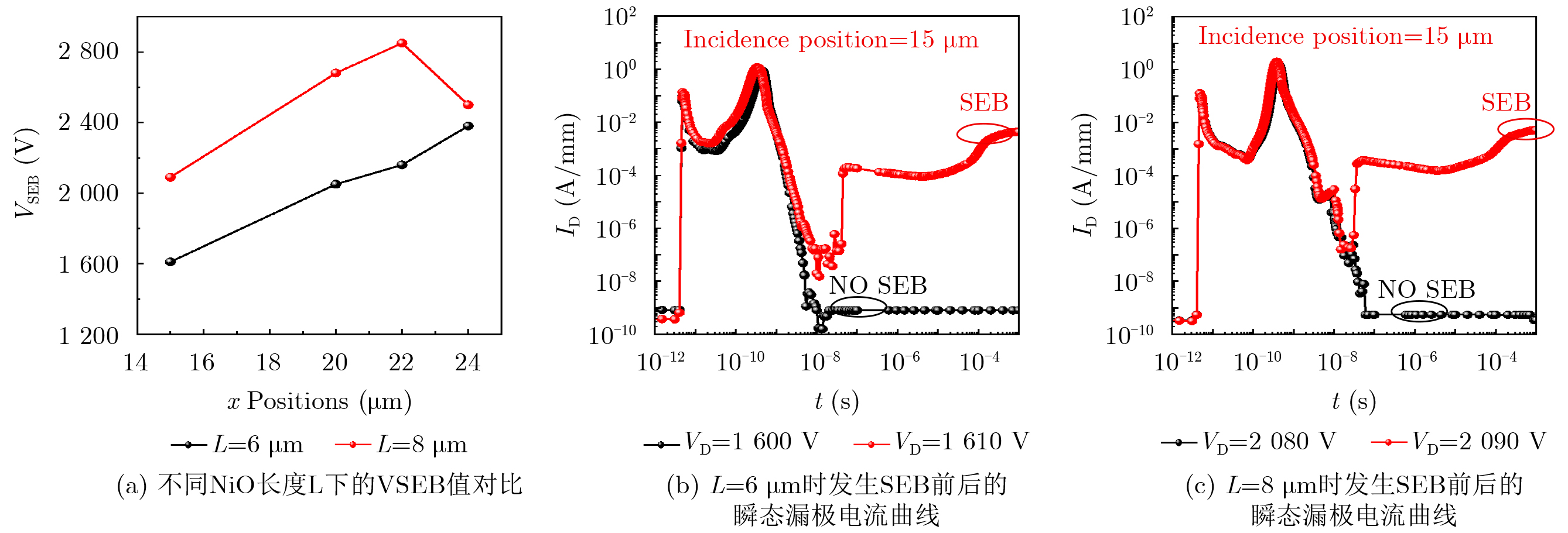
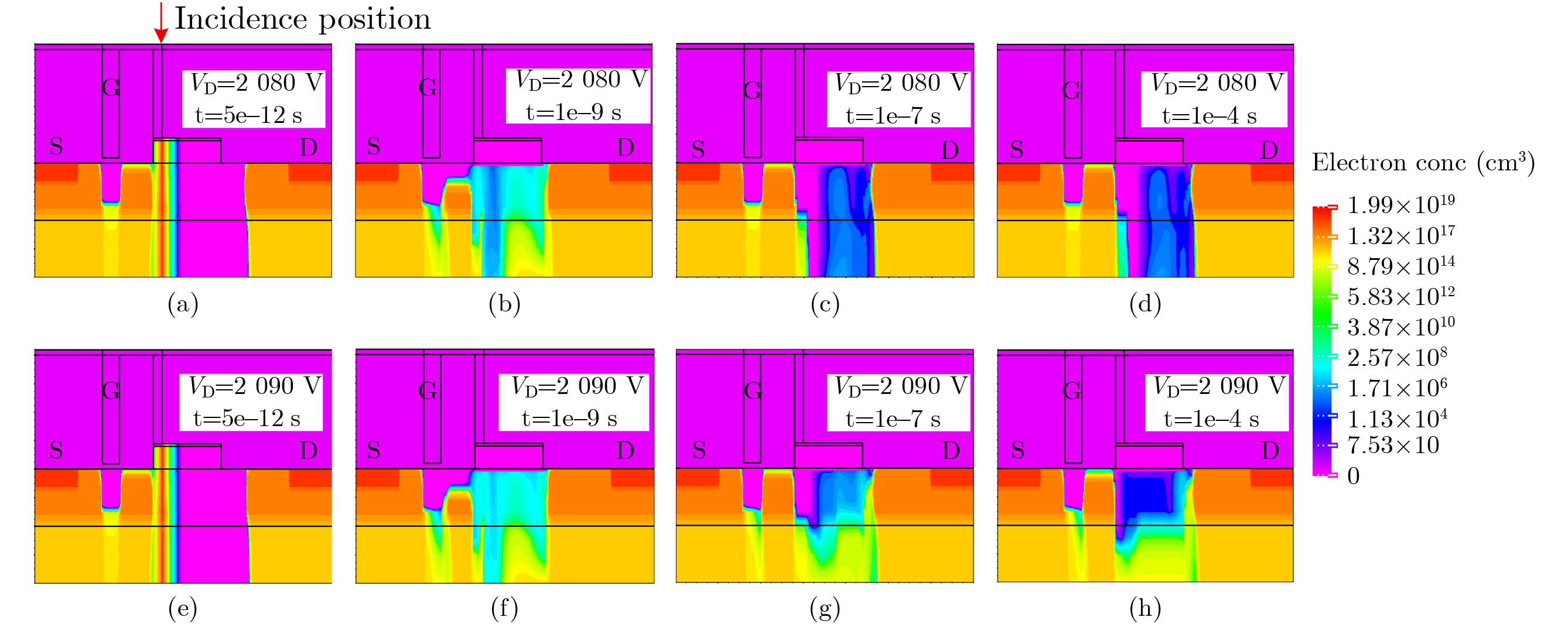
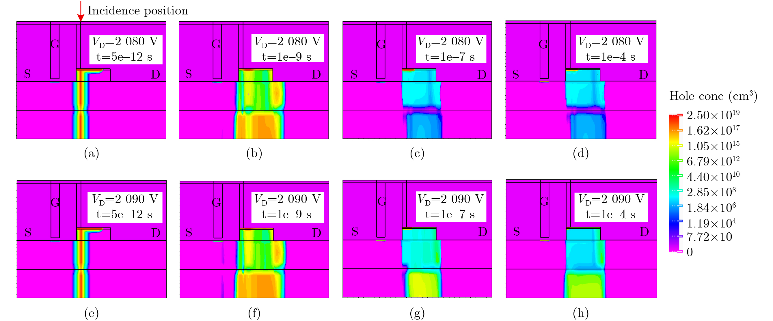
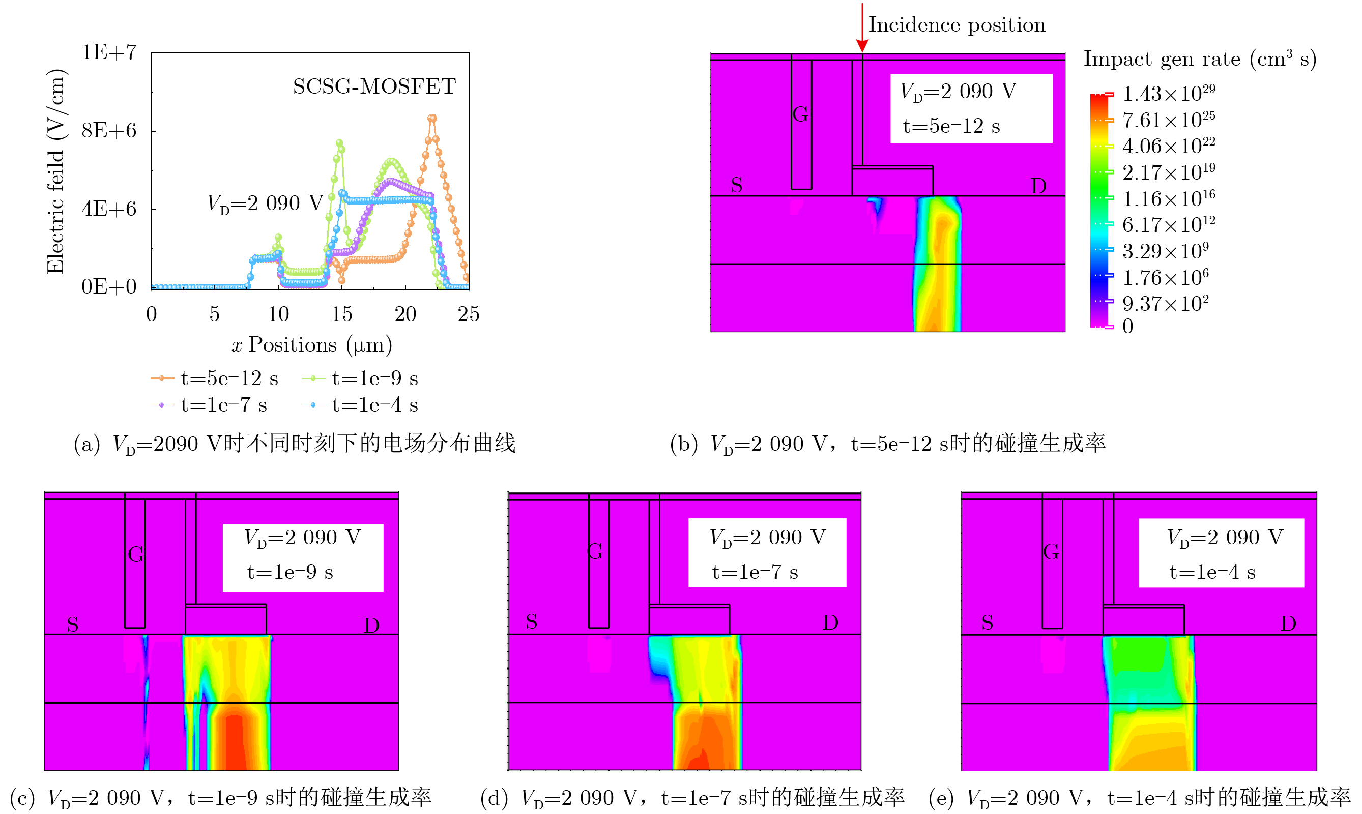
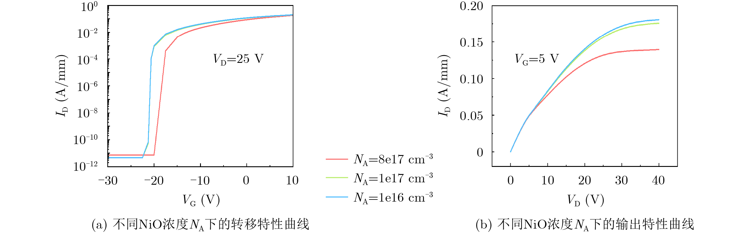
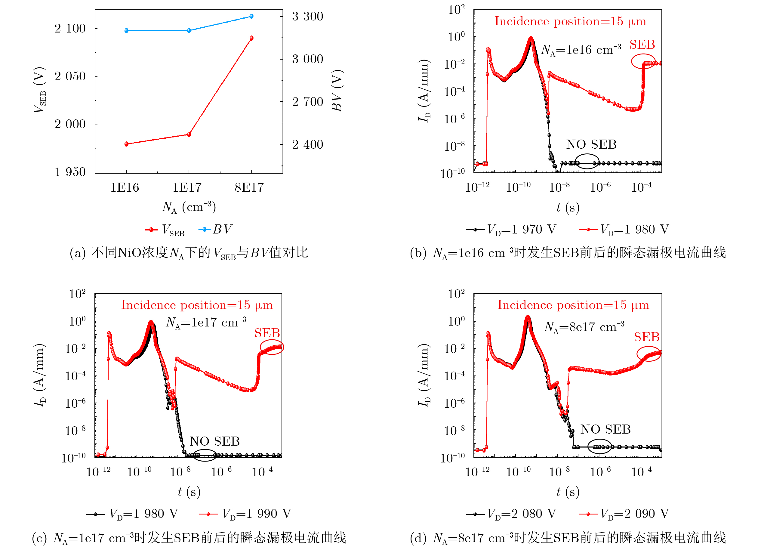
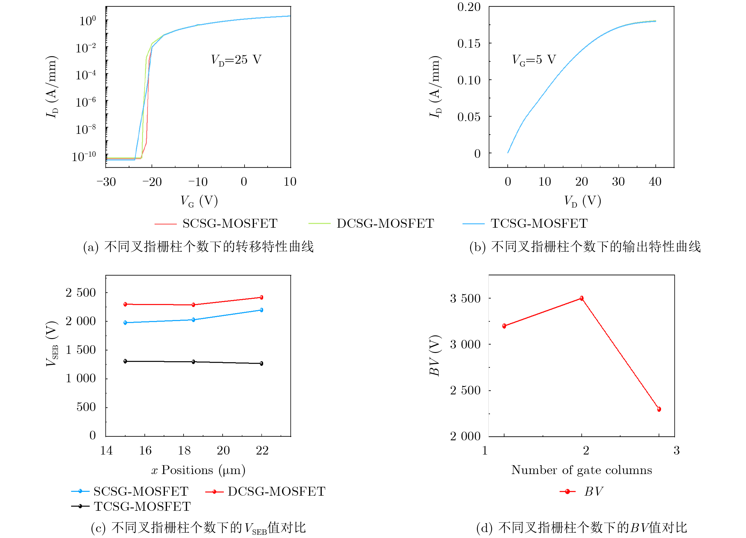
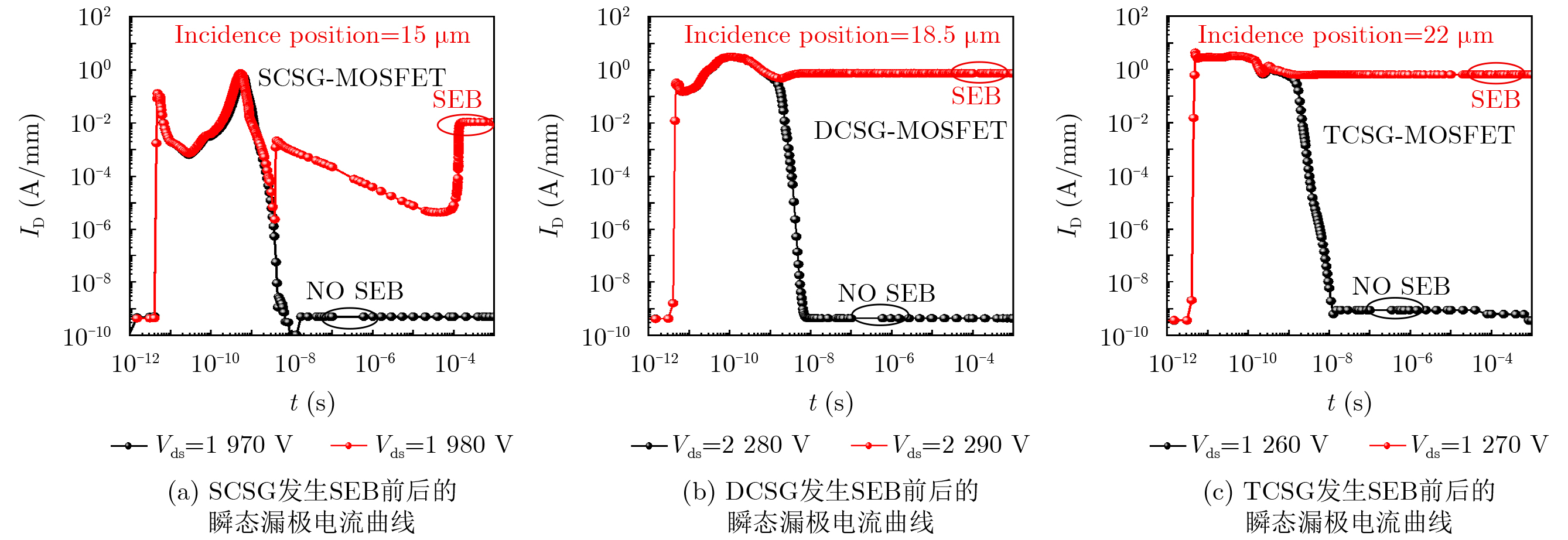
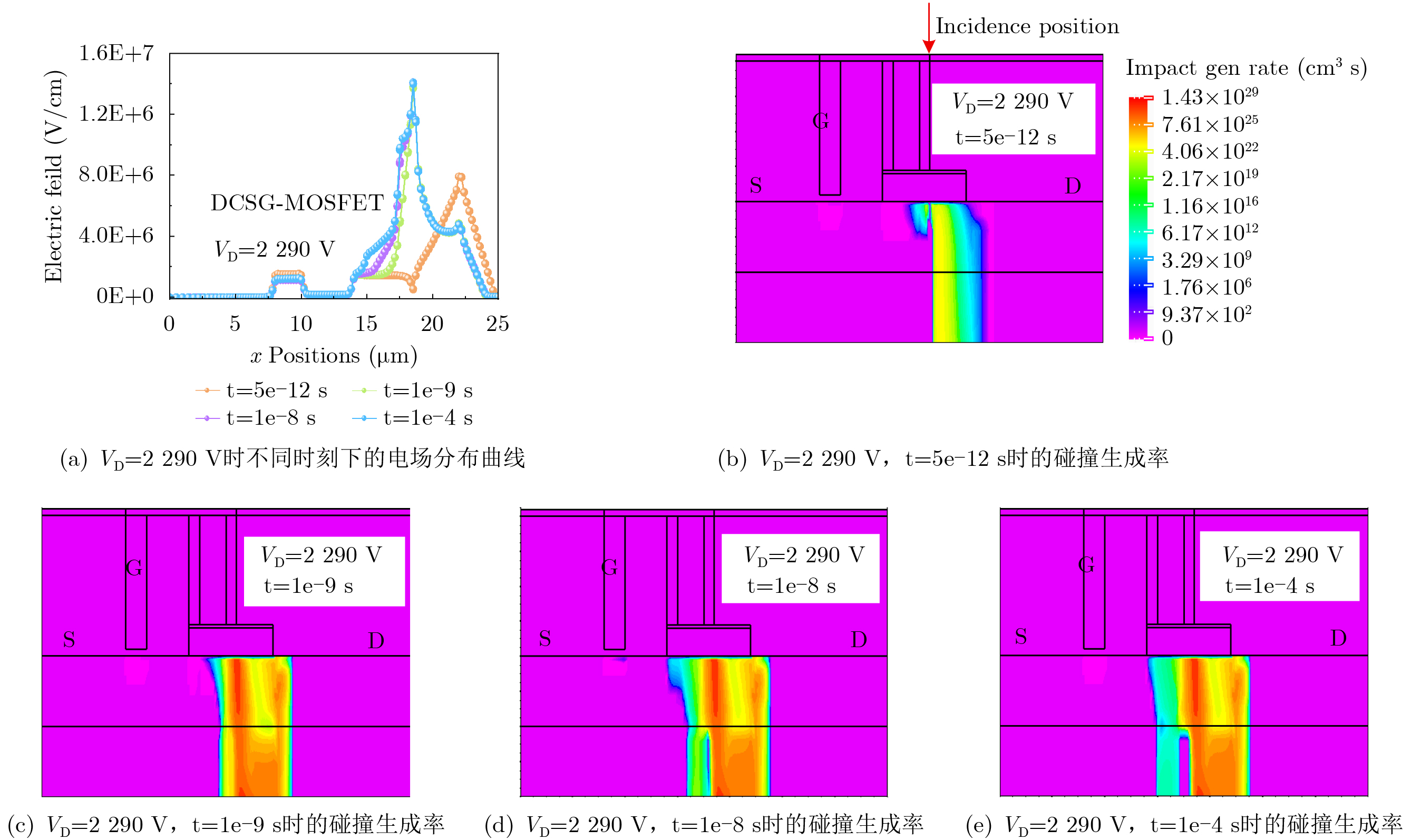
  •   Objective  Gallium Oxide Metal-Oxide-Semiconductor Field-Effect Transistor (Ga2O3 MOSFET) is considered a promising power device for high-voltage applications, particularly in space power systems such as aerospace and satellite platforms, owing to its ultra-wide bandgap and high critical breakdown field. However, the Conventional Ga2O3 MOSFET (C-MOSFET) exhibits significant drawbacks when operating in space radiation environments. Under off-state conditions, the electric field distribution within the channel region is highly concentrated, particularly at the gate edge, where localized strong electric fields form. When a high-energy heavy ion strikes the device, a large number of electron-hole pairs are generated along the ion track. Under the influence of the strong electric field, these carriers undergo multiplication effects, causing the drain current to surge dramatically and fail to recover, ultimately leading to irreversible Single-Event Burnout (SEB) even at relatively low drain biases. This phenomenon represents one of the primary failure modes for power devices in space applications, severely limiting the reliable deployment of Ga2O3 MOSFETs in harsh radiation environments. Furthermore, the difficulty in achieving reliable and efficient P-type doping in Ga2O3 inherently limits the application of conventional radiation-hardening techniques such as junction termination extensions and junction isolation in Ga2O3 devices. The difficulty in achieving reliable and efficient P-type doping in Ga2O3 makes ionized charges more prone to accumulation in sensitive regions, further exacerbating the device’s susceptibility to Single-Event Effects (SEE). Meanwhile, the extremely low thermal conductivity of Ga2O3 causes Joule heat generated by transient currents to accumulate locally without effective dissipation. Within an extremely short time after heavy-ion incidence, heat concentrates in a microscopic region, forming localized hot spots that significantly increase the risk of thermal-induced burnout. To address these issues, existing hardening approaches such as field plates and dielectric layer optimization provide certain improvements in device robustness, yet research on the application of heterojunction structures for radiation hardening in Ga2O3 MOSFETs remains relatively limited, and systematic hardening solutions have yet to be established. While field plates can alleviate the peak electric field at the gate edge, their capability to dissipate transient carriers generated by heavy-ion incidence is limited. Dielectric layer optimization primarily improves the reliability of the gate dielectric but offers weak modulation of the internal electric field within the channel. To address these issues, this paper proposes a radiation-hardened Ga2O3 MOSFET featuring a NiO heterojunction and Comb-Shaped Gate (CSG) column structure, which optimizes the electric field distribution within the channel region, alleviates the electric field crowding effect at the conventional gate edge, and significantly enhances the device’s SEB robustness, providing an effective solution for Ga2O3 power devices in harsh radiation environments.  Methods  TCAD simulations are employed to evaluate the electrical characteristics and SEB performance of the proposed CSG-MOSFET, in comparison with the C-MOSFET. A range of physical models is incorporated in the simulations, including high-field mobility saturation, Shockley-Read-Hall and Auger recombination, impact ionization, and heavy-ion incidence. Based on the charge compensation mechanism in the space charge region of a PN junction, the proposed heterojunction structure leverages the depletion region formed between the P-type NiO layer and the N-type Ga2O3 channel to achieve effective modulation of the electric field distribution. The heterojunction utilizes the extension of the depletion region at the interface to create a barrier area within the channel, thereby optimizing the internal field profile and enhancing the device’s robustness against SEB. Furthermore, the CSG columns, in conjunction with the extended gate field plate, reconfigure the location of the peak electric field away from the conventional gate edge, alleviating local field concentration and improving device reliability under high-voltage and radiation-hard environments.  Results and Discussions  Simulation results show that compared to the C-MOSFET, the proposed CSG-MOSFET significantly enhances SEB tolerance. The SEB threshold voltage (VSEB) increases from 240 V to 2280 V, and the Breakdown Voltage (BV) improves from 2000 V to 3500 V, while the specific on-resistance is reduced. Consequently, the Baliga figure of merit and the SEB-based figure of merit are dramatically improved. The NiO heterojunction and CSG columns effectively modulate the electric field distribution, relocating the peak field from the gate edge to the gate column edge and alleviating local field concentration, thereby significantly improving radiation hardness.  Conclusions  In this paper, a novel radiation-hardened Ga2O3 MOSFET design featuring a NiO heterojunction and CSG column structure is proposed through TCAD simulation. The proposed structure significantly enhances SEB tolerance. The VSEB and BV are substantially increased compared to the C-MOSFET, demonstrating superior blocking capability. Due to the charge compensation effect between the P-type NiO layer and the N-type Ga2O3 channel, the heterojunction forms an extended depletion region that effectively modulates the electric field distribution within the channel. This modulation alleviates the electric field crowding effect at the conventional gate edge. Furthermore, the CSG columns, in conjunction with the extended gate field plate, actively relocate the peak electric field from the gate edge to the outermost gate column edge. This electric field reconfiguration reduces carrier multiplication effects upon heavy-ion incidence, thereby effectively suppressing SEB. The specific on-resistance is also reduced, leading to improved Baliga figure of merit and SEB-based figure of merit. These advantages make the proposed CSG-MOSFET a promising candidate for power electronics applications in harsh radiation environments such as aerospace and satellite platforms.
  • loading
  • [1]
    ATMACA G and CHA H Y. Normally-off recessed gate β-Ga2O3 MOSHFETs with a modulation-doped heterostructure back-barrier[J]. Physica Scripta, 2024, 99(3): 035901. doi: 10.1088/1402-4896/ad213f.
    [2]
    HASAN A S M K, HOSSAIN M M, HERIS P C, et al. Single event upset in depletion-mode gallium oxide MOSFETs at the breakdown region[C]. 2024 IEEE Applied Power Electronics Conference and Exposition (APEC), Long Beach, USA, 2024: 2461–2467. doi: 10.1109/APEC48139.2024.10509030.
    [3]
    WONG M H, TAKEYAMA A, MAKINO T, et al. Radiation hardness of β-Ga2O3 metal-oxide-semiconductor field-effect transistors against gamma-ray irradiation[J]. Applied Physics Letters, 2018, 112(2): 023503. doi: 10.1063/1.5017810.
    [4]
    WANG Kejia, WANG Zujun, CAO Rongxin, et al. Study of the mechanism of single event burnout in lateral depletion-mode Ga2O3 MOSFET devices via TCAD simulation[J]. Journal of Applied Physics, 2024, 135(14): 145702. doi: 10.1063/5.0184704.
    [5]
    KONG Moufu, YANG Mingliang, DENG Hongfei, et al. A novel lateral superjunction Ga2O3 MOSFET with a self-biased accumulation layer for ultra-low specific on-resistance and improved FOM[J]. Semiconductor Science and Technology, 2025, 40(4): 045009. doi: 10.1088/1361-6641/adc1fd.
    [6]
    GOYAL P and KAUR H. Implementing variable doping and work function engineering in β-Ga2O3 MOSFET to realize high breakdown voltage and PfoM[J]. Semiconductor Science and Technology, 2022, 37(4): 045018. doi: 10.1088/1361-6641/ac5843.
    [7]
    WANG Chenlu, YAN Qinglong, SU Chunxu, et al. Demonstration of the β-Ga2O3 MOS-JFETs with suppressed gate leakage current and large gate swing[J]. IEEE Electron Device Letters, 2023, 44(3): 380–383. doi: 10.1109/LED.2023.3237598.
    [8]
    YOU Jinle, LIAO Fei, MA Zepeng, et al. High-performance lateral enhancement-mode β-Ga2O3 MOSFET with a novel superjunction-extended gate structure[J]. Semiconductor Science and Technology, 2025, 40(8): 085004. doi: 10.1088/1361-6641/adf661.
    [9]
    MA Hongye, WANG Wentao, CAI Yuncong, et al. Analysis of single event effects by heavy ion irradiation of Ga2O3 metal-oxide-semiconductor field-effect transistors[J]. Journal of Applied Physics, 2023, 133(8): 085701. doi: 10.1063/5.0107325.
    [10]
    WANG Zefeng, LIU Fengkai, LIU Zhongli, et al. Simulation of the single-event burnout in lateral enhancement-mode β-Ga2O3 MOSFET devices[J]. IEEE Transactions on Device and Materials Reliability, 2026, 26(1): 351–357. doi: 10.1109/TDMR.2026.3658196.
    [11]
    YU Chenghao, GUO Haomin, LIU Yan, et al. Simulation study on single-event burnout in field-plated Ga2O3 MOSFETs[J]. Microelectronics Reliability, 2023, 149: 115227. doi: 10.1016/j.microrel.2023.115227.
    [12]
    LEI Weina, DANG Kui, ZHOU Hong, et al. Proposal and simulation of Ga2O3 MOSFET with PN heterojunction structure for high-performance E-mode operation[J]. IEEE Transactions on Electron Devices, 2022, 69(7): 3617–3622. doi: 10.1109/TED.2022.3172919.
    [13]
    HUANG Jiaweiwen, CHEN Wensuo, ZHAO Shenglei, et al. High performance E-mode NiO/β-Ga2O3 HJ-FET with high conduction band offset and thin recessed channel[J]. Micro and Nanostructures, 2024, 195: 207963. doi: 10.1016/j.micrna.2024.207963.
    [14]
    MIAO Ruixia, JI Xiang, WANG Jiaqi, et al. Single event effect of E-mode Ga2O3 heterojunction field effect transistor under heavy ion irradiation[C]. 2025 4th International Symposium on Semiconductor and Electronic Technology (ISSET), Xi’an, China, 2025: 633–638. doi: 10.1109/ISSET66828.2025.11185020.
    [15]
    WANG Wentao, CAI Yuncong, TIAN Xusheng, et al. Simulation research on high-voltage β-Ga2O3 MOSFET based on floating field plate[J]. ECS Journal of Solid State Science and Technology, 2024, 13(2): 025002. doi: 10.1149/2162-8777/ad28c9.
    [16]
    DATTA A and SINGISETTI U. Simulation studies of single-event effects in β-Ga2O3 MOSFETs[J]. IEEE Transactions on Electron Devices, 2024, 71(1): 476–483. doi: 10.1109/TED.2023.3330132.
    [17]
    HAN Yixin, LUO Zixiang, WANG Jialin, et al. Simulation research on a Ga2O3-based superjunction field effect transistor[J]. ECS Journal of Solid State Science and Technology, 2025, 14(7): 075002. doi: 10.1149/2162-8777/adeae4.
  • 加载中

Catalog

    通讯作者: 陈斌, bchen63@163.com
    • 1. 

      沈阳化工大学材料科学与工程学院 沈阳 110142

    1. 本站搜索
    2. 百度学术搜索
    3. 万方数据库搜索
    4. CNKI搜索

    Figures(17)  / Tables(2)

    Article Metrics

    Article views (62) PDF downloads(4) Cited by()
    Proportional views
    Related

    /

    DownLoad:  Full-Size Img  PowerPoint
    Return
    Return