| Citation: | LIU Ming, ZHAO Yaqi, GUAN Xiaoning, ZHANG Fan, LU Pengfei. Research Status and Prospects of Mid-Wavelength Infrared Superlattice Detector Technology[J]. Journal of Electronics & Information Technology. doi: 10.11999/JEIT260083

|

| [1] |
SAI-HALASZ G A, TSU R, and ESAKI L. A new semiconductor superlattice[J]. Applied Physics Letters, 1977, 30(12): 651–653. doi: 10.1063/1.89273.
|
| [2] |
MAILHIOT C and SMITH D L. Electronic structure of (001) and (111) growth axis InAs-Ga1-x InxSb strained-layer superlattices[J]. Journal of Vacuum Science & Technology B: Microelectronics Processing and Phenomena, 1987, 5(4): 1268–1273. doi: 10.1116/1.583817.
|
| [3] |
杨雪艳, 孙童, 关晓宁, 等. T2SL红外探测器高量子效率机理的研究进展[J]. 激光技术, 2024, 48(6): 822–831. doi: 10.7510/jgjs.issn.1001-3806.2024.06.007.
YANG Xueyan, SUN Tong, GUAN Xiaoning, et al. Research progress on the high quantum efficiency mechanism of T2SL infrared detectors[J]. Laser Technology, 2024, 48(6): 822–831. doi: 10.7510/jgjs.issn.1001-3806.2024.06.007.
|
| [4] |
ALSHAHRANI D O, KESARIA M, ANYEBE E A, et al. Emerging type-II superlattices of InAs/InAsSb and InAs/GaSb for mid-wavelength infrared photodetectors[J]. Advanced Photonics Research, 2022, 3(2): 2100094. doi: 10.1002/adpr.202100094.
|
| [5] |
ROGALSKI A. New ternary alloy systems for infrared detectors[C]. SPIE 1845, Liquid and Solid State Crystals: Physics, Technology and Applications, Zakopane, Poland, 1993: 52–60. doi: 10.1117/12.156938.
|
| [6] |
WANG Xiaohua, LI Jingzhen, YAN Yong, et al. Dark current analysis of InAs/GaSb type II superlattice infrared detectors[J]. IEEE Transactions on Electron Devices, 2023, 70(11): 5517–5527. doi: 10.1109/ted.2023.3314574.
|
| [7] |
JONES R C. Performance of detectors for visible and infrared radiation[J]. Advances in Electronics and Electron Physics, 1953, 5: 1–96. doi: 10.1016/s0065-2539(08)60683-6.
|
| [8] |
SHI Qian, ZHANG Shukui, WANG Jianlu, et al. Progress on nBn infrared detectors[J]. Journal of Infrared and Millimeter Waves, 2022, 41(1): 139–150. doi: 10.11972/j.issn.1001-9014.2022.01.010.
|
| [9] |
KLIPSTEIN P C, BENNY Y, COHEN Y, et al. XBn and XBp detectors based on type II superlattices[J]. Journal of Electronic Materials, 2022, 51(9): 4752–4757. doi: 10.1007/s11664-022-09661-0.
|
| [10] |
KLIPSTEIN P C. Perspective on III-V barrier detectors[J]. Applied Physics Letters, 2022, 120(6): 060502. doi: 10.1063/5.0084100.
|
| [11] |
LI Mingluo, GUAN Xiaoning, YANG Xueyan, et al. nBp-type InAs/InAsSb midwave infrared detector with multistep absorption[J]. Infrared Physics & Technology, 2026, 152: 106159. doi: 10.1016/j.infrared.2025.106159.
|
| [12] |
JIANG Junkai, CHANG Faran, ZHOU Wenguang, et al. High-performance extended short-wavelength infrared PBn photodetectors based on InAs/GaSb/AlSb superlattices[J]. Chinese Physics B, 2023, 32(3): 038503. doi: 10.1088/1674-1056/acaa2e.
|
| [13] |
MARCHEWKA M, JAROSZ D, RUSZAŁA M, et al. Interfaces-engineered M-structure for infrared detectors[J]. Opto-Electronics Review, 2024, 32(2): e150183. doi: 10.24425/opelre.2024.150183.
|
| [14] |
TING D Z, SOIBEL A, KHOSHAKHLAGH A, et al. Complementary barrier infrared detector architecture for long-wavelength infrared InAs/InAsSb type-II superlattice[J]. Applied Sciences, 2022, 12(24): 12508. doi: 10.3390/app122412508.
|
| [15] |
TING D Z, SOIBEL A, KHOSHAKHLAGH A, et al. Mid-wavelength high operating temperature barrier infrared detector and focal plane array[J]. Applied Physics Letters, 2018, 113(2): 021101. doi: 10.1063/1.5033338.
|
| [16] |
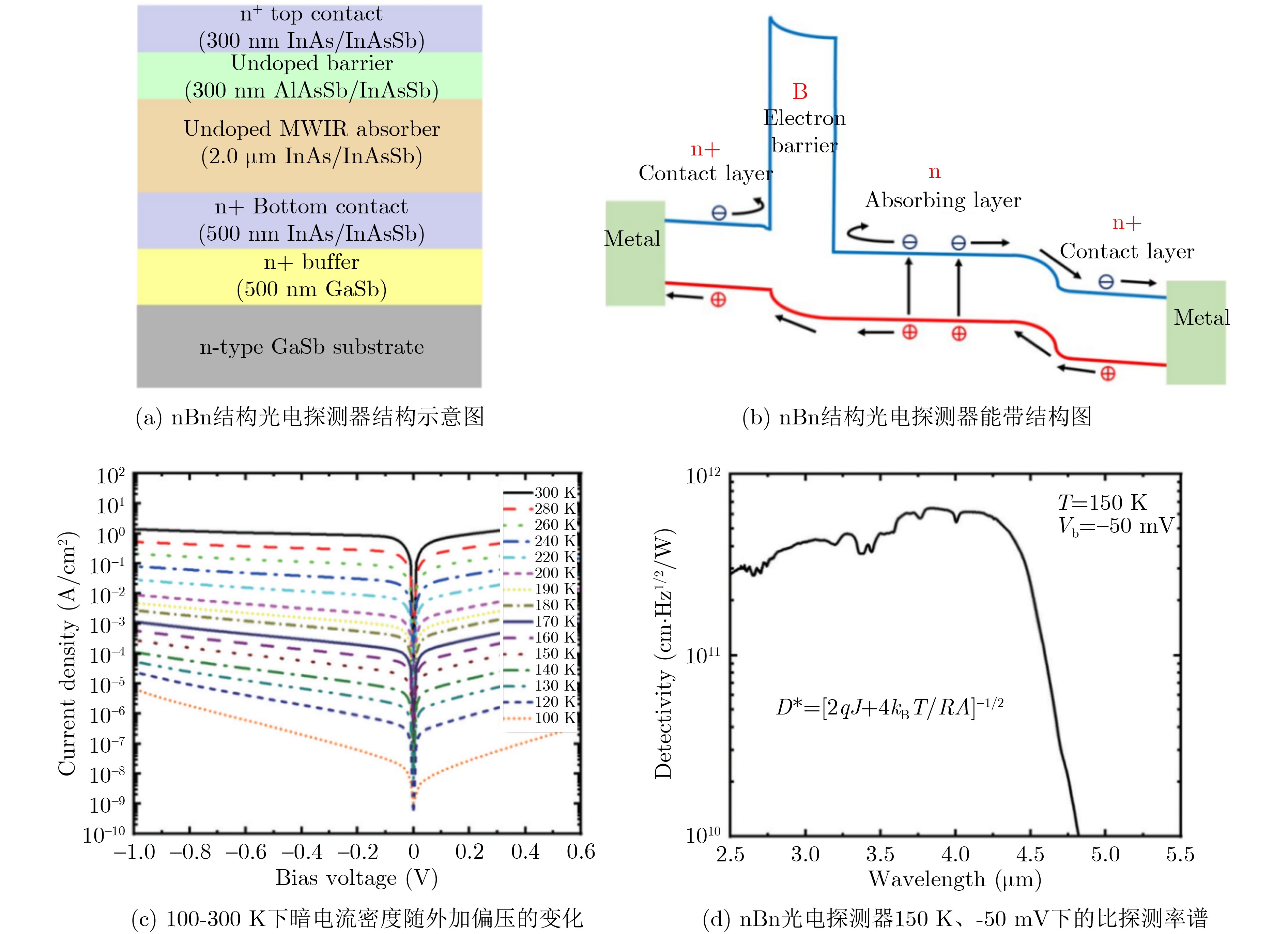
单一凡, 吴东海, 谢若愚, 等. 基于AlAsSb/InAsSb超晶格势垒的InAs/InAsSb Ⅱ类超晶格nBn中波红外探测器[J]. 红外与毫米波学报, 2024, 43(4): 450–456. doi: 10.11972/j.issn.1001-9014.2024.04.003.
SHAN Yifan, WU Donghai, XIE Ruoyu, et al. Mid-wavelength infrared nBn photodetectors based on InAs/InAsSb type-II superlattice with an AlAsSb/InAsSb superlattice barrier[J]. Journal of Infrared and Millimeter Waves, 2024, 43(4): 450–456. doi: 10.11972/j.issn.1001-9014.2024.04.003.
|
| [17] |
LEE H J, KO S Y, KIM Y H, et al. Strain-induced the dark current characteristics in InAs/GaSb type-II superlattice for mid-wave detector[J]. Journal of Semiconductors, 2020, 41(6): 062302. doi: 10.1088/1674-4926/41/6/062302.
|
| [18] |
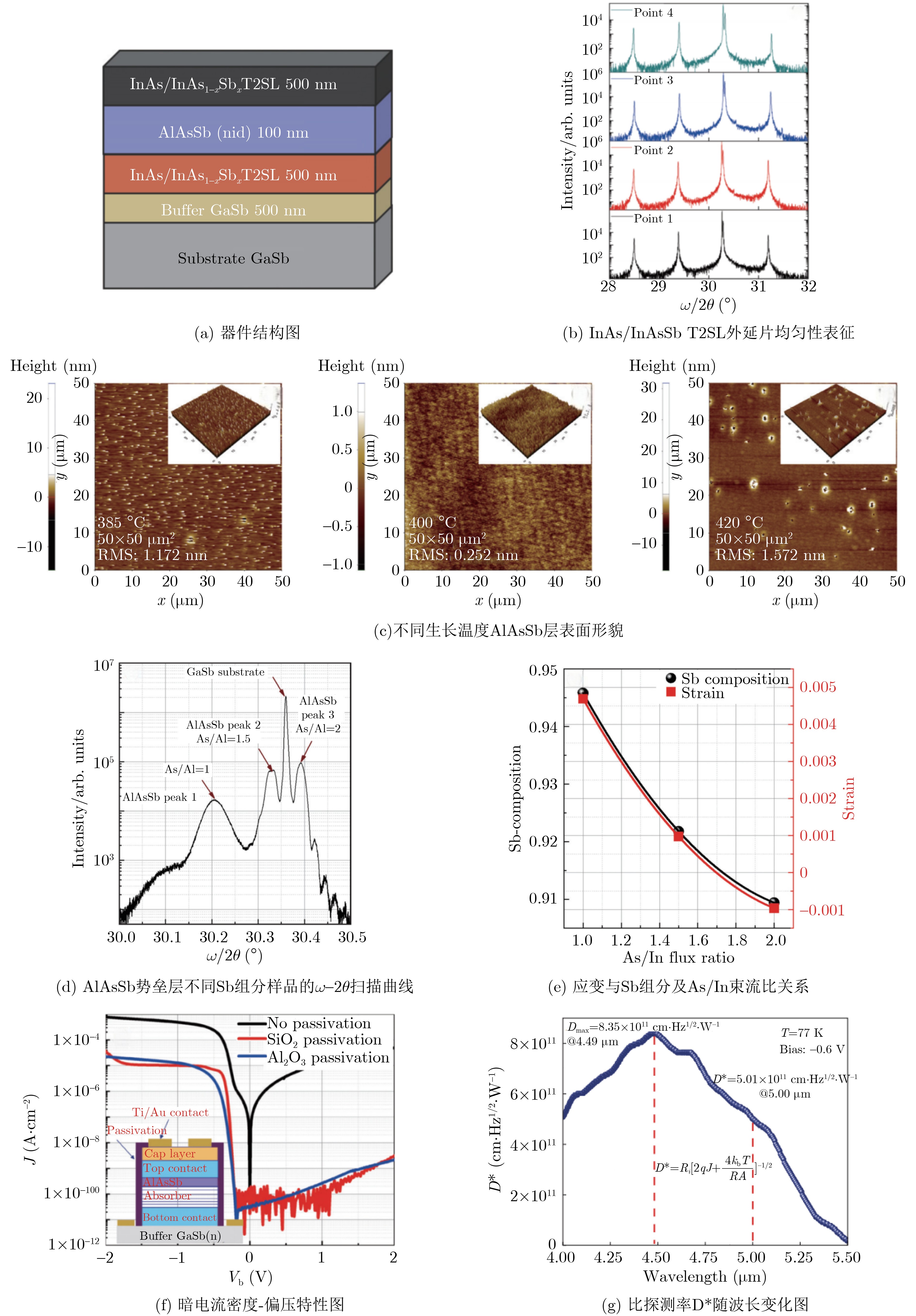
刘炳锋, 祝连庆, 鹿利单, 等. 中波InAs/InAsSb超晶格红外探测器设计及势垒外延优化制备[J]. 红外与激光工程, 2025, 54(8): 20250340. doi: 10.3788/IRLA20250340.
LIU Bingfeng, ZHU Lianqing, LU Lidan, et al. Design of mid-wavelength InAs/InAsSb superlattice infrared detectors and barrier epitaxial optimization[J]. Infrared and Laser Engineering, 2025, 54(8): 20250340. doi: 10.3788/IRLA20250340.
|
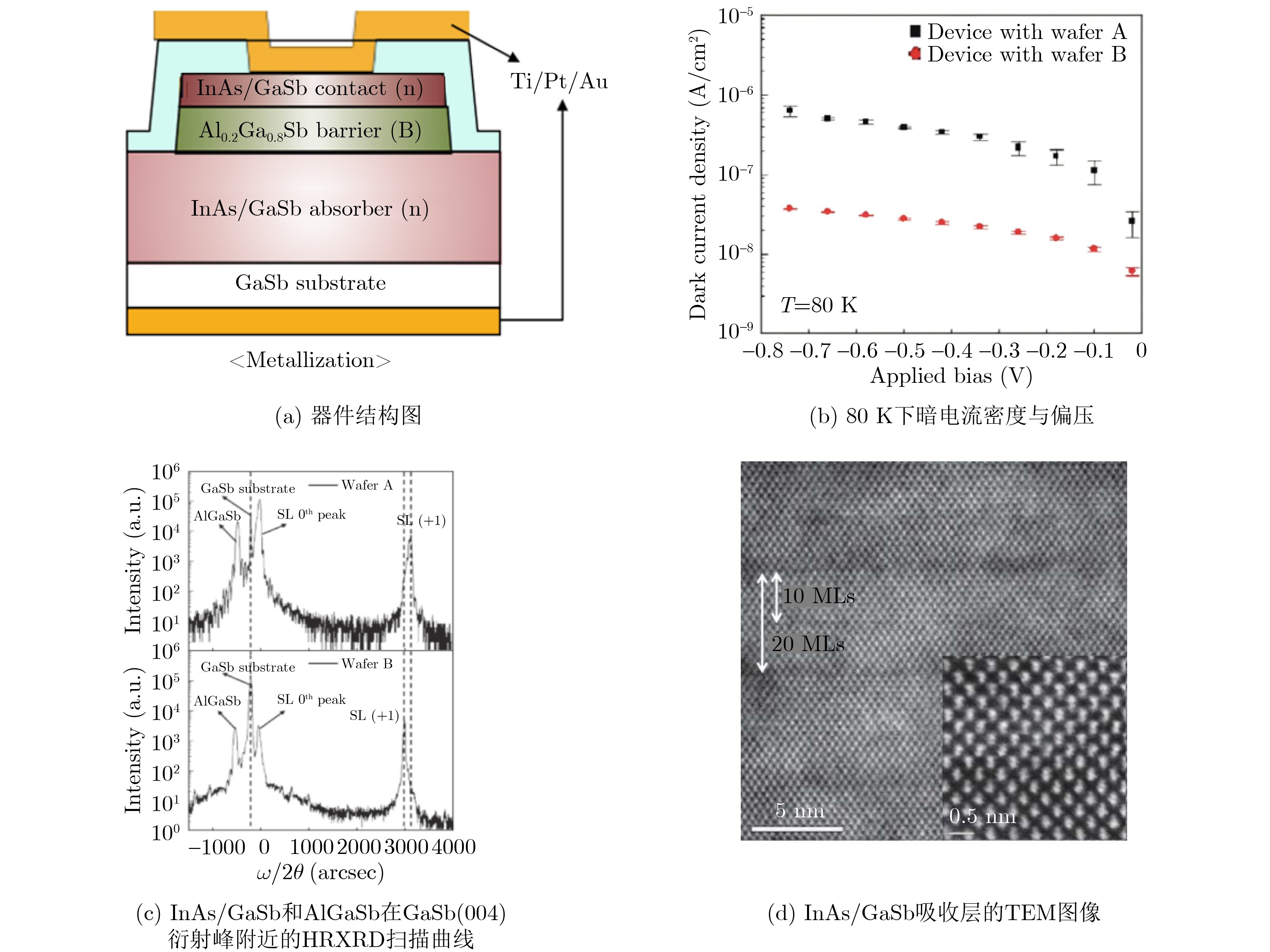
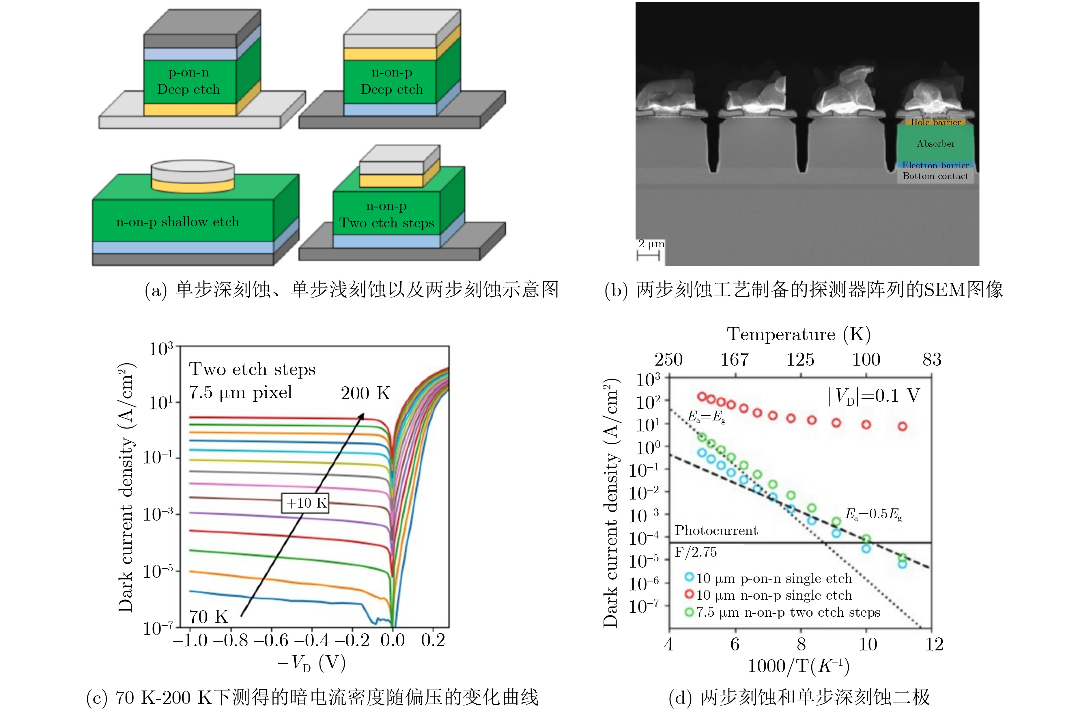
| [19] |
RAMOS D, DELMAS M, IVANOV R, et al. Two-step etch in n-on-p type-II superlattices for surface leakage reduction in mid-wave infrared megapixel detectors[J]. Opto-Electronics Review, 2023, 31(S1): e144556. doi: 10.24425/opelre.2023.144556.
|
| [20] |
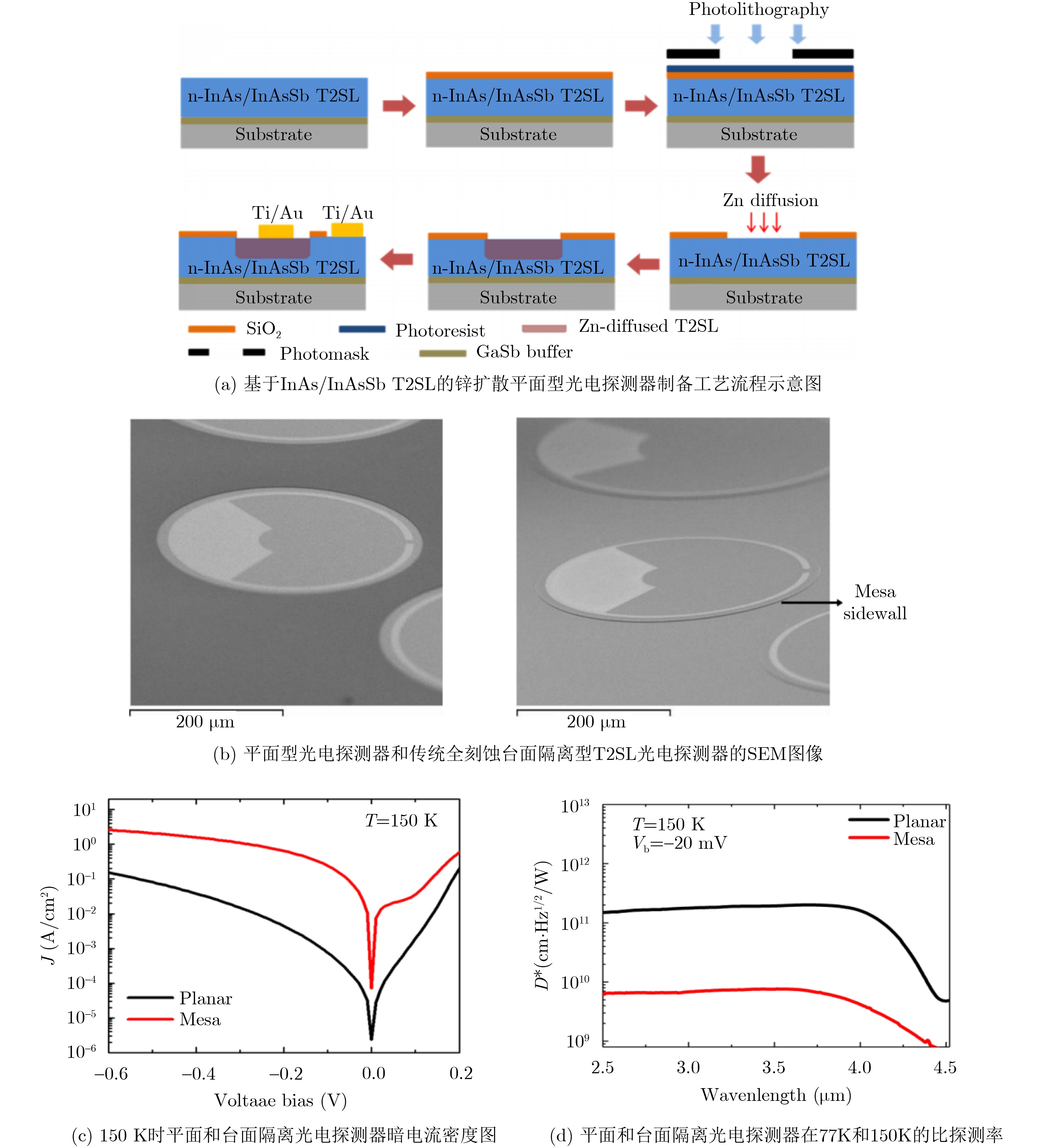
LI Jiakai, SAROJ R K, SLIVKEN S, et al. High performance planar antimony-based superlattice photodetectors using zinc diffusion grown by MBE[J]. Photonics, 2022, 9(9): 664. doi: 10.3390/photonics9090664.
|
| [21] |
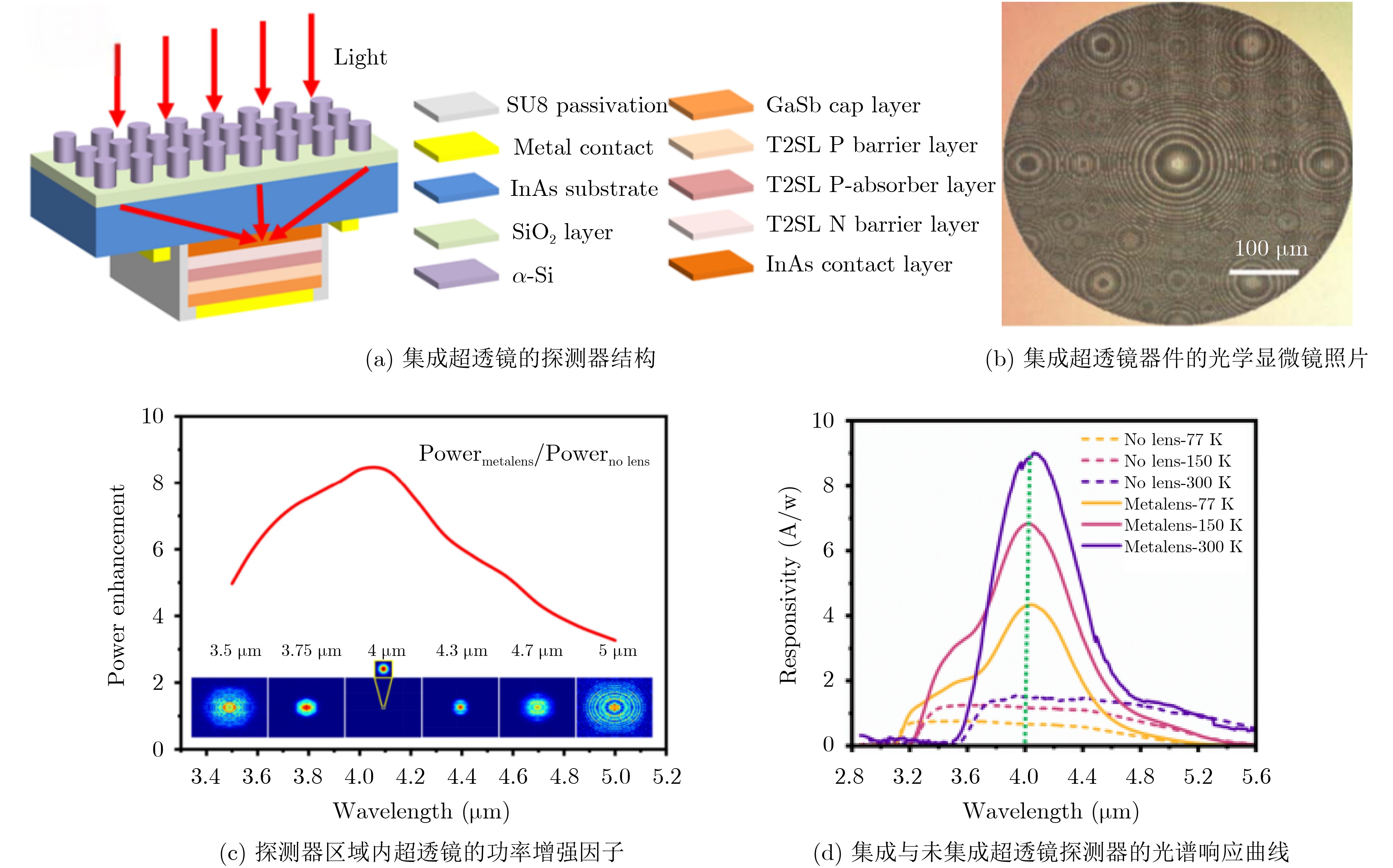
YUE Jiaxin, ZHANG Jinyu, QIN Le, et al. Enhancing mid-wavelength InAs/GaSb type II superlattice infrared detector with monolithically integrated metalens[J]. Optics Express, 2025, 33(15): 30948–30956. doi: 10.1364/OE.568141.
|
| [22] |
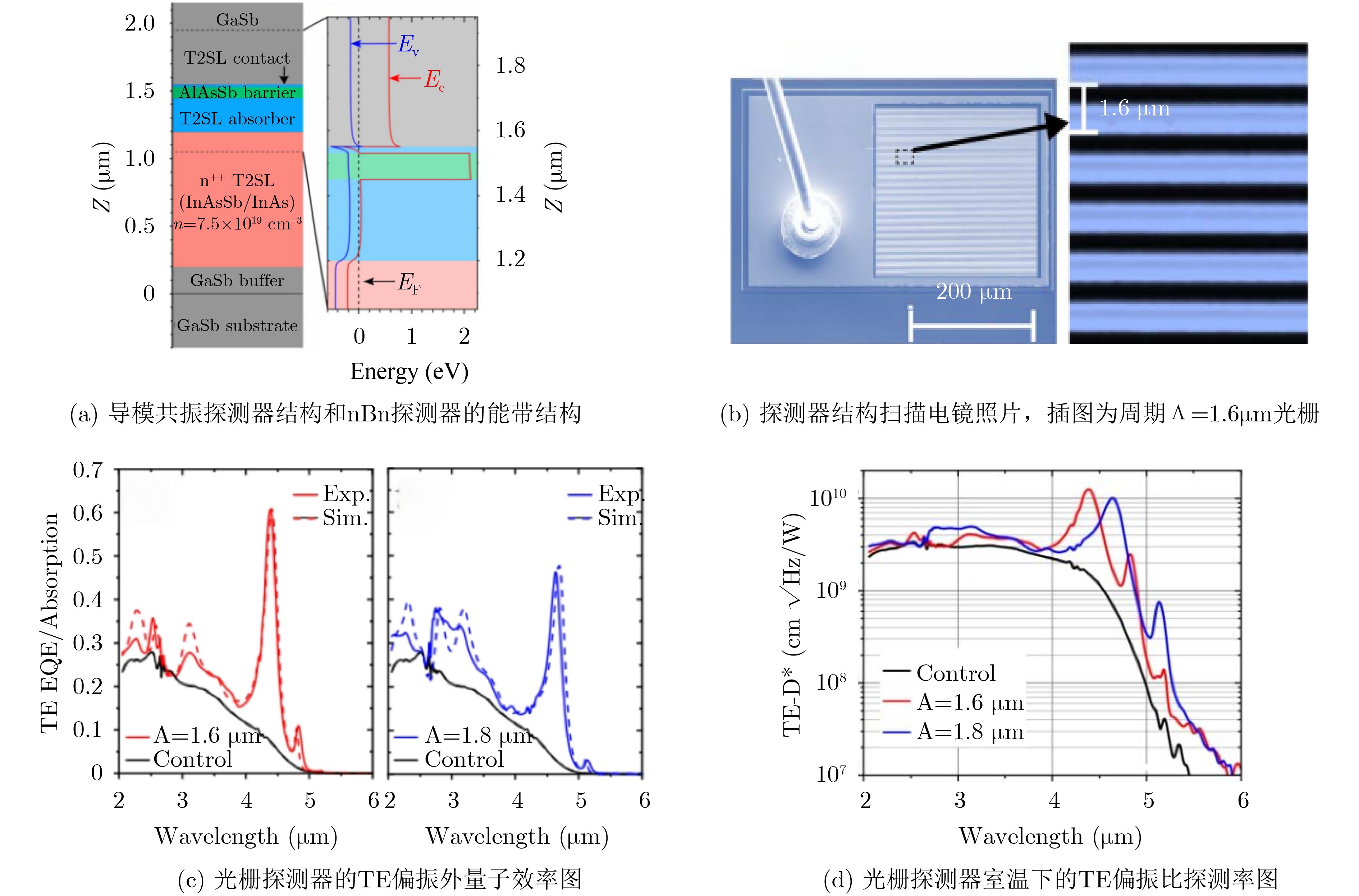
KAMBOJ A, NORDIN L, MUHOWSKI A J, et al. Room-temperature mid-wave infrared guided-mode resonance detectors[J]. IEEE Photonics Technology Letters, 2022, 34(11): 615–618. doi: 10.1109/LPT.2022.3175110.
|
| [23] |
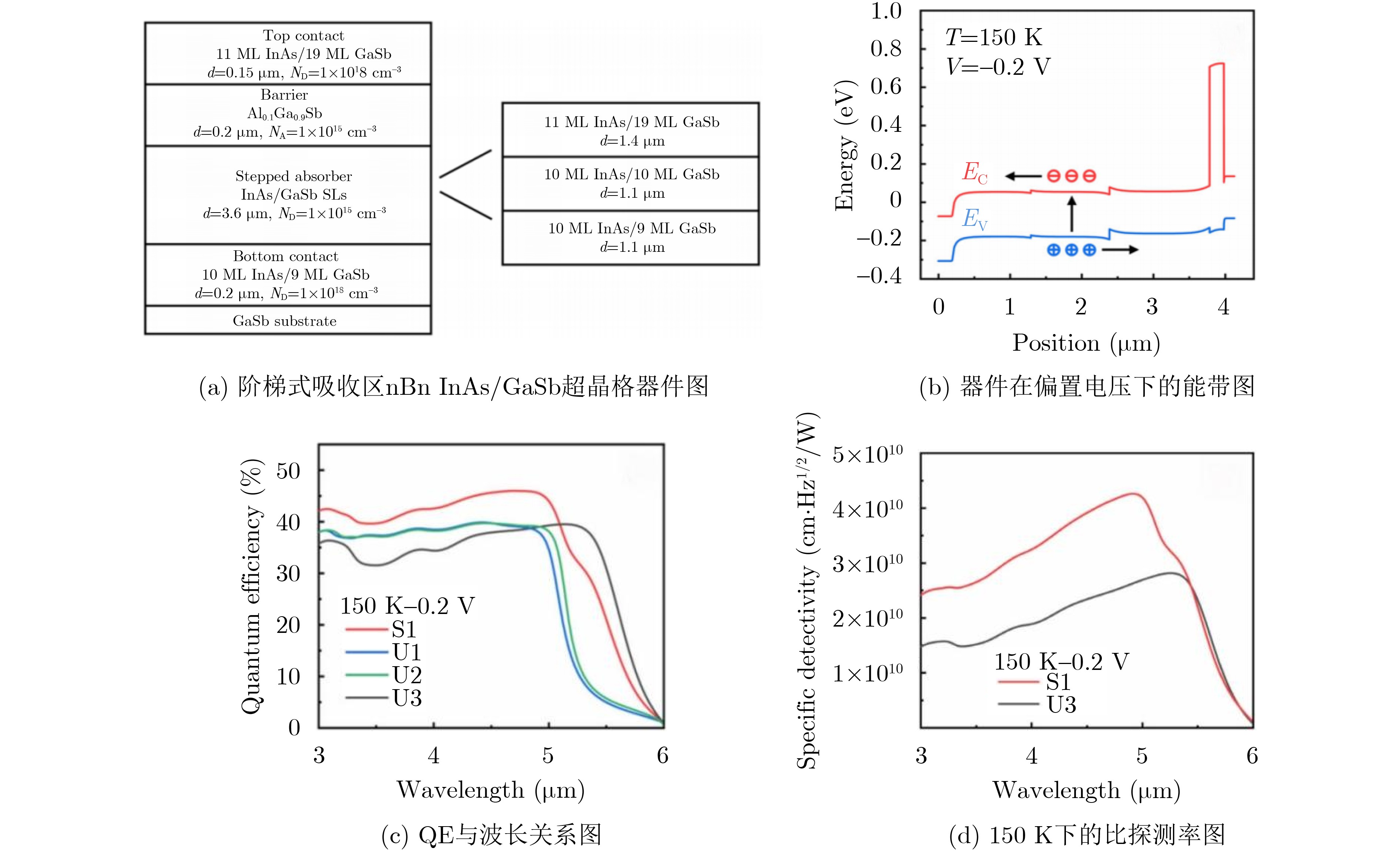
YUAN Qi, LI Chuang, GUO Daqian, et al. High-performance midwave type-II superlattice infrared photodetectors with a stepped InAs/GaSb absorber[J]. IEEE Transactions on Electron Devices, 2023, 70(5): 2347–2351. doi: 10.1109/TED.2023.3256965.
|
| [24] |
ZHANG Ye, SHAN Yifan, CHANG Faran, et al. High operating temperature mid-wavelength infrared detectors based on InAs/InAsSb superlattices with electron block interfacial graded doping[J]. Optics Express, 2025, 33(17): 36672–36681. doi: 10.1364/oe.572457.
|
| [25] |
WU Yuyang, ZHANG Yahui, ZHANG Yi, et al. Dual strategy of modulating growth temperature and inserting ultrathin barrier to enhance the wave function overlap in type-II superlattices[J]. Nano Research, 2022, 15(6): 5626–5632. doi: 10.1007/s12274-022-4151-7.
|
| [26] |
MILOSAVLJEVIC M S, CARRASCO R A, NEWELL A T, et al. Spectroscopic ellipsometry measurement and analysis of the optical constants of InAs/InAsSb and InGaAs/InAsSb superlattices and their bulk constituents[J]. Journal of Applied Physics, 2025, 138(9): 093103. doi: 10.1063/5.0285129.
|
| [27] |
LEE H J, KIM Y C, EOM J H, et al. Development of MWIR and LWIR nBn photodetectors at i3system[C]. SPIE 12107, Infrared Technology and Applications XLVIII, Orlando, United States, 2022: 1210713. doi: 10.1117/12.2607715.
|
| [28] |
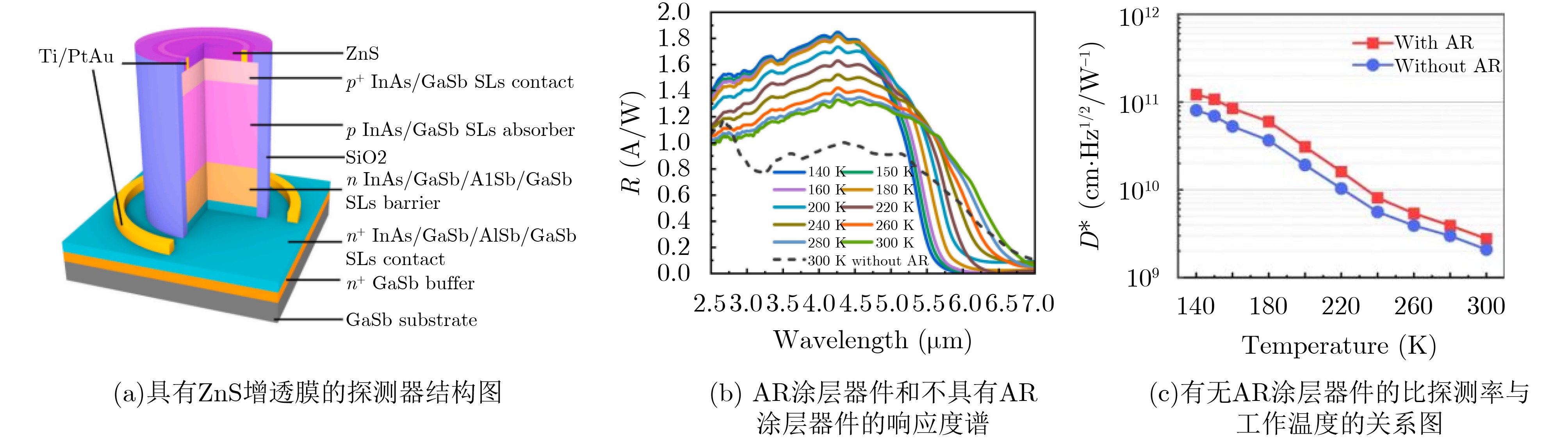
YAO Lingze, SHAN Yifan, XIE Ruoyu, et al. Room-temperature mid-wave infrared InAs/GaSb type-II superlattice photodetectors enhanced by ZnS anti-reflection coating[J]. Optical Materials, 2025, 165: 117155. doi: 10.1016/j.optmat.2025.117155.
|
| [29] |
ZHANG Shihao, HAO Hongyue, ZHANG Ye, et al. Mid-wavelength infrared planar junction photodetector based on InAs/GaSb Type-II superlattices[J]. Journal of Semiconductors, 2025, 46(11): 112404. doi: 10.1088/1674-4926/24120014.
|
| [30] |
ASPLUND C, MARCKS VON WÜRTEMBERG R, LANTZ D, et al. Performance of mid-wave T2SL detectors with heterojunction barriers[J]. Infrared Physics & Technology, 2013, 59: 22–27. doi: 10.1016/j.infrared.2012.12.004.
|
| [31] |
DELMAS M, DEBNATH M C, LIANG Baolai, et al. Material and device characterization of Type-II InAs/GaSb superlattice infrared detectors[J]. Infrared Physics & Technology, 2018, 94: 286–290. doi: 10.1016/j.infrared.2018.09.012.
|
| [32] |
HÖGLUND L, ASPLUND C, MARCKS VON WÜRTEMBERG R, et al. Manufacturability of type-II InAs/GaSb superlattice detectors for infrared imaging[J]. Infrared Physics & Technology, 2017, 84: 28–32. doi: 10.1016/j.infrared.2017.03.002.
|
| [33] |
DURLIN Q, PEREZ J P, CERUTTI L, et al. Midwave infrared barrier detector based on Ga-free InAs/InAsSb type-II superlattice grown by molecular beam epitaxy on Si substrate[J]. Infrared Physics & Technology, 2019, 96: 39–43. doi: 10.1016/j.infrared.2018.10.006.
|
| [34] |
WU Donghai, DURLIN Q, DEHZANGI A, et al. High quantum efficiency mid-wavelength infrared type-II InAs/InAs1-xSbx superlattice photodiodes grown by metal-organic chemical vapor deposition[J]. Applied Physics Letters, 2019, 114(1): 011104. doi: 10.1063/1.5058714.
|
| [35] |
SHE Lifang, JIANG Junkai, CHEN Weiqiang, et al. Mid-wave infrared p+-B-n InAs/InAsSb type-II superlattice photodetector with an AlAsSb/InAsSb superlattice barrier[J]. Infrared Physics & Technology, 2022, 121: 104015. doi: 10.1016/j.infrared.2021.104015.
|
| [36] |
CAO Peng, WANG Tiancai, PENG Hongling, et al. Mid-wavelength nBn photodetector with high operating temperature and low dark current based on InAs/InAsSb superlattice absorber[J]. Chinese Optics Letters, 2024, 22(1): 012502. doi: 10.3788/col202422.012502.
|
| [37] |
刘炳锋, 祝连庆, 鹿利单, 等. nBn型高温中波InAs/InAsSb超晶格红外焦平面探测器[J]. 光学学报, 2025, 45(7): 0712001. doi: 10.3788/AOS241909.
LIU Bingfeng, ZHU Lianqing, LU Lidan, et al. High operating temperature InAs/InAsSb Type-II superlattice mid-wave infrared nBn focal plane detectors[J]. Acta Optica Sinica, 2025, 45(7): 0712001. doi: 10.3788/AOS241909.
|
| [38] |
BOUSCHET M, AROUNASSALAME V, RAMIANDRASOA A, et al. Temperature dependence study of electrical and electro-optical performances of midwave infrared Ga-free T2SL barrier photodetector[J]. Applied Sciences, 2022, 12(20): 10358. doi: 10.3390/app122010358.
|
| [39] |
TING D Z, SOIBEL A, KHOSHAKHLAGH A, et al. The effect of p-doping in mid-and long-wavelength InAs/InAsSb superlattice complementary barrier infrared detectors[J]. Applied Physics Letters, 2024, 125(19): 191106. doi: 10.1063/5.0236130.
|
| [40] |
SUN Yaoyao, WANG Guowei, HAN Xi, et al. 320×256 high operating temperature mid-infrared focal plane arrays based on type-II InAs/GaSb superlattice[J]. Superlattices and Microstructures, 2017, 111: 783–788. doi: 10.1016/j.spmi.2017.07.037.
|
| [41] |
JIANG Junkai, WANG Guowei, WU Donghai, et al. High-performance infrared photodetectors based on InAs/InAsSb/AlAsSb superlattice for 3.5 µm cutoff wavelength spectra[J]. Optics Express, 2022, 30(21): 38208–38215. doi: 10.1364/OE.469147.
|
| [42] |
DELMAS M, HÖGLUND L, IVANOV R, et al. HOT SWaP and HD detectors based on Type-II superlattices at IRnova[C]. SPIE 12107, Infrared Technology and Applications XLVIII, Orlando, United States, 2022: 121070R. doi: 10.1117/12.2618752.
|
| [43] |
HAO Ruiting, REN Yang, LIU Sijia, et al. Fabrication and characterization of high lattice matched InAs/InAsSb superlattice infrared photodetector[J]. Journal of Crystal Growth, 2017, 470: 33–36. doi: 10.1016/j.jcrysgro.2017.03.052.
|
| [44] |
TING D Z, RAFOL S B, KEO S A, et al. InAs/InAsSb type-II superlattice mid-wavelength infrared focal plane array with significantly higher operating temperature than InSb[J]. IEEE Photonics Journal, 2018, 10(6): 6804106. doi: 10.1109/JPHOT.2018.2877632.
|
| [45] |
KLIPSTEIN P C, ARMON E, AVNON E, et al. HOT MWIR technology at SCD[C]. SPIE 12107, Infrared Technology and Applications XLVIII, Orlando, United States, 2022: 121070Q. doi: 10.1117/12.2615622.
|
| [46] |
KOPYTKO M, MADEJCZYK P, MURAWSKI K, et al. Comparison of type II superlattice InAs/InAsSb barrier detectors operating in the mid-wave infrared range[J]. Journal of Applied Physics, 2024, 136(1): 014501. doi: 10.1063/5.0202170.
|
| [47] |
HUANG Jianliang, YAN Shaolong, XUE Ting, et al. Mid-wavelength InAs/InAsSb superlattice photodetector with background limited performance temperature higher than 160 K[J]. IEEE Transactions on Electron Devices, 2022, 69(8): 4392–4395. doi: 10.1109/TED.2022.3186648.
|
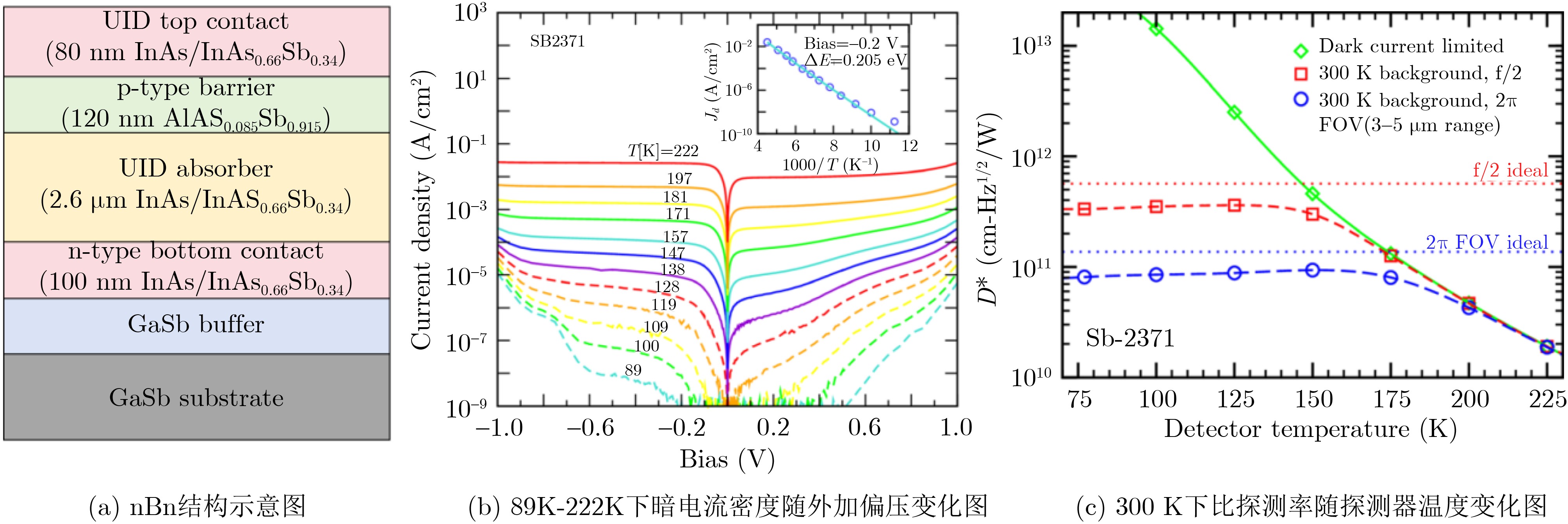
Figures(17) / Tables(2)


 DownLoad: