Advanced Search
Turn off MathJax
Article Contents
DOU Xianrui, LIANG Huaguo, HUANG Zhengfeng, LU Yingchun, CHEN Tian, LIU Jun. MOS-gated Prebond Through-Silicon Via Testing[J]. Journal of Electronics & Information Technology. doi: 10.11999/JEIT250285
Citation: DOU Xianrui, LIANG Huaguo, HUANG Zhengfeng, LU Yingchun, CHEN Tian, LIU Jun. MOS-gated Prebond Through-Silicon Via Testing[J]. Journal of Electronics & Information Technology. doi: 10.11999/JEIT250285

MOS-gated Prebond Through-Silicon Via Testing

doi: 10.11999/JEIT250285 cstr: 32379.14.JEIT250285
Funds:  The National Natural Science Foundation of China (62027815, 62174048, 62274052), The Key Project of Teaching Reform Research for Postgraduate Education in Anhui Province (2022jyjxggyj053), The Ministry of Education, Industry-University-Research Co-Operation Collaborative Education Project (220802455302758)
  • Received Date: 2025-04-17
  • Rev Recd Date: 2025-07-28
  • Available Online: 2025-08-04
  •   Objective  As the miniaturization of semiconductor chips approaches physical limitations, integrated chip technologies have become essential to meet the demand for high-performance, low-cost devices in the post-Moore era. Through-Silicon Via (TSV) is a key process in advanced packaging that requires precise testing to ensure reliable interconnections. Quantitative test methods can estimate defect sizes based on test responses; however, variations in Process, Voltage, and Temperature (PVT) hinder accurate defect characterization, making the associated overhead of data capture and analysis difficult to justify. Current techniques often require long test time, with some necessitating two test cycles. While leakage defect detection has reached high accuracy, the detection of resistive open defects—sometimes only tens of milliohms in fault-free states—remains inadequate. This study presents a method that improves detection accuracy for resistive open defects and reduces both test area and time overhead, offering a more efficient and practical TSV testing solution.  Methods  Previous studies indicate that rising-edge testing provides higher resolution than falling-edge testing and enables simultaneous differentiation of multiple defect types. Based on this principle, a symmetric testing scheme through a single rising-edge test is proposed. To reduce the area overhead associated with shared test structures, MOS gates are employed as selection switches. NMOS transistors, due to their strong 0 and weak 1 characteristics, are placed at the driving end to enable rapid discharge and reset of the reference capacitor voltage. PMOS transistors, exhibiting strong 1 and weak 0 characteristics, are positioned at the receiving end to block interference from low-voltage signals. A two-stage comparator is then employed to amplify the voltage difference between the reference capacitor and the test TSV during the charging phase, producing two intermediate voltage levels. These are subsequently converted into standard high or low logic levels by a Schmitt trigger inverter. Based on the output logic level, both the presence and type of defect can be determined from a single test.  Results and Discussions  The effectiveness of the proposed method is verified through HSPICE simulations using the Nangate 45 nm open cell library. The detection accuracy for different defect types is modulated by adjusting the Width-to-Length (W/L) ratio of the MOS transistors, as shown in (Table 2). For instance, reducing the W/L ratio of NMOS transistors enhances the detection sensitivity to leakage defects. Specific W/L ratios can therefore be selected to meet targeted testing requirements. (Table 3) presents the results under PVT variations. Although the accuracy shows minor fluctuations, these remain within acceptable limits. A temperature variation of approximately 27 °C results in only a 1 Ω deviation in resistive open defect detection, and a 1 MΩ range in leakage defect accuracy. Even under the worst-case PVT condition, the minimum detection threshold for resistive open defects reaches 94 Ω, which exceeds the capability of existing methods.  Conclusions  A prebond TSV testing scheme based on MOS gating is proposed to address the high area and time overheads and limited accuracy of conventional approaches. The scheme adopts a symmetric structure between the reference capacitor and the test TSV to mitigate capacitance variation caused by fabrication inconsistencies. A two-stage comparator amplifies the voltage difference between the defective TSV and the reference capacitor during charging, thereby enhancing detection resolution. Simulation results indicate that the method detects resistive open defects equal of above 50 Ω and leakage defects equal of below 9 MΩ. Compared with existing methods, the proposed approach significantly reduces both testing area and time. When multiple TSVs share the testing circuitry, only one NMOS and one PMOS transistor are added, further minimizing the average area overhead.
  • loading
  • [1]
    DEBENEDICTIS E P, BADAROGLU M, CHEN An, et al. Sustaining Moore’s law with 3D chips[J]. Computer, 2017, 50(8): 69–73. doi: 10.1109/MC.2017.3001236.
    [2]
    THADESAR P A, GU Xiaoxiong, ALAPATI R, et al. Through-silicon Vias: Drivers, performance, and innovations[J]. IEEE Transactions on Components, Packaging and Manufacturing Technology, 2016, 6(7): 1007–1017. doi: 10.1109/TCPMT.2016.2524691.
    [3]
    HWANG Y, MOON S, NAM S, et al. Chiplet-based system PSI optimization for 2.5D/3D advanced packaging implementation[C]. 2022 IEEE 72nd Electronic Components and Technology Conference (ECTC), San Diego, USA, 2022: 12–17. doi: 10.1109/ECTC51906.2022.00010.
    [4]
    LAU J H. Recent advances and trends in multiple system and heterogeneous integration with TSV interposers[J]. IEEE Transactions on Components, Packaging and Manufacturing Technology, 2023, 13(1): 3–25. doi: 10.1109/TCPMT.2023.3234007.
    [5]
    LAU J H. Recent advances and trends in advanced packaging[J]. IEEE Transactions on Components, Packaging and Manufacturing Technology, 2022, 12(2): 228–252. doi: 10.1109/TCPMT.2022.3144461.
    [6]
    JUNG D H, KIM Y, KIM J J, et al. Through Silicon Via (TSV) defect modeling, measurement, and analysis[J]. IEEE Transactions on Components, Packaging and Manufacturing Technology, 2017, 7(1): 138–152. doi: 10.1109/TCPMT.2016.2631731.
    [7]
    ZHAO Yi, KHURSHEED S, and AL-HASHIMI B M. Online fault tolerance technique for TSV-based 3-D-IC[J]. IEEE Transactions on Very Large Scale Integration (VLSI) Systems, 2015, 23(8): 1567–1571. doi: 10.1109/TVLSI.2014.2343156.
    [8]
    CHANDRAKAR M and MAJUMDER M K. Performance analysis using air gap defected through silicon via: Impact on crosstalk and power[J]. IEEE Transactions on Components, Packaging and Manufacturing Technology, 2022, 12(11): 1832–1840. doi: 10.1109/TCPMT.2022.3225142.
    [9]
    XU Kangkang, YU Yang, and FANG Xu. The detection of open and leakage faults for Prebond TSV test based on weak current source[J]. IEEE Transactions on Computer-Aided Design of Integrated Circuits and Systems, 2022, 41(9): 2768–2779. doi: 10.1109/TCAD.2021.3114357.
    [10]
    LIU Jun, CHENG Songren, CHEN Tian, et al. A self-biased current reference source-based pre-bond TSV test solution[J]. IEEE Transactions on Very Large Scale Integration (VLSI) Systems, 2024, 32(4): 774–781. doi: 10.1109/TVLSI.2023.3344272.
    [11]
    DAS S, SU F, and CHAKRAVARTY S. A PVT-resilient no-touch DFT methodology for prebond TSV testing[C]. 2018 IEEE International Test Conference (ITC), Phoenix, USA, 2018: 1–10. doi: 10.1109/TEST.2018.8624691.
    [12]
    YI Maoxiang, BIAN Jingchang, NI Tianming, et al. A pulse shrinking-based test solution for Prebond through silicon via in 3-D ICs[J]. IEEE Transactions on Computer-Aided Design of Integrated Circuits and Systems, 2019, 38(4): 755–766. doi: 10.1109/TCAD.2018.2821559.
    [13]
    LIU Jun, CHEN Zhi, CHEN Tian, et al. Voltage skew-based test technique for pre-bond TSVs in 3-D ICs[J]. IEEE Transactions on Circuits and Systems II: Express Briefs, 2024, 71(8): 3930–3934. doi: 10.1109/TCSII.2024.3373897.
    [14]
    WANG Lihang, DONG Gang, ZHI Changle, et al. Prebond TSV detection for coexistence of open and leakage faults based on current charging and discharging[J]. IEEE Transactions on Components, Packaging and Manufacturing Technology, 2025, 15(5): 1091–1103. doi: 10.1109/TCPMT.2025.3543693.
    [15]
    CHANG Hao, HUANG Zhengfeng, and NI Tianming. Kelvin bridge structure based TSV test for weak faults[C]. 2021 IEEE International Test Conference in Asia (ITC-Asia), Shanghai, China, 2021: 1–6. doi: 10.1109/ITC-Asia53059.2021.9808492.
    [16]
    LIU Jun, CHEN Zhi, CHENG Songren, et al. A symmetric bridge-based pre-bond TSV faults detection method[J]. IEEE Transactions on Instrumentation and Measurement, 2024, 73: 2004710. doi: 10.1109/TIM.2024.3427774.
  • 加载中

Catalog

    通讯作者: 陈斌, bchen63@163.com
    • 1. 

      沈阳化工大学材料科学与工程学院 沈阳 110142

    1. 本站搜索
    2. 百度学术搜索
    3. 万方数据库搜索
    4. CNKI搜索

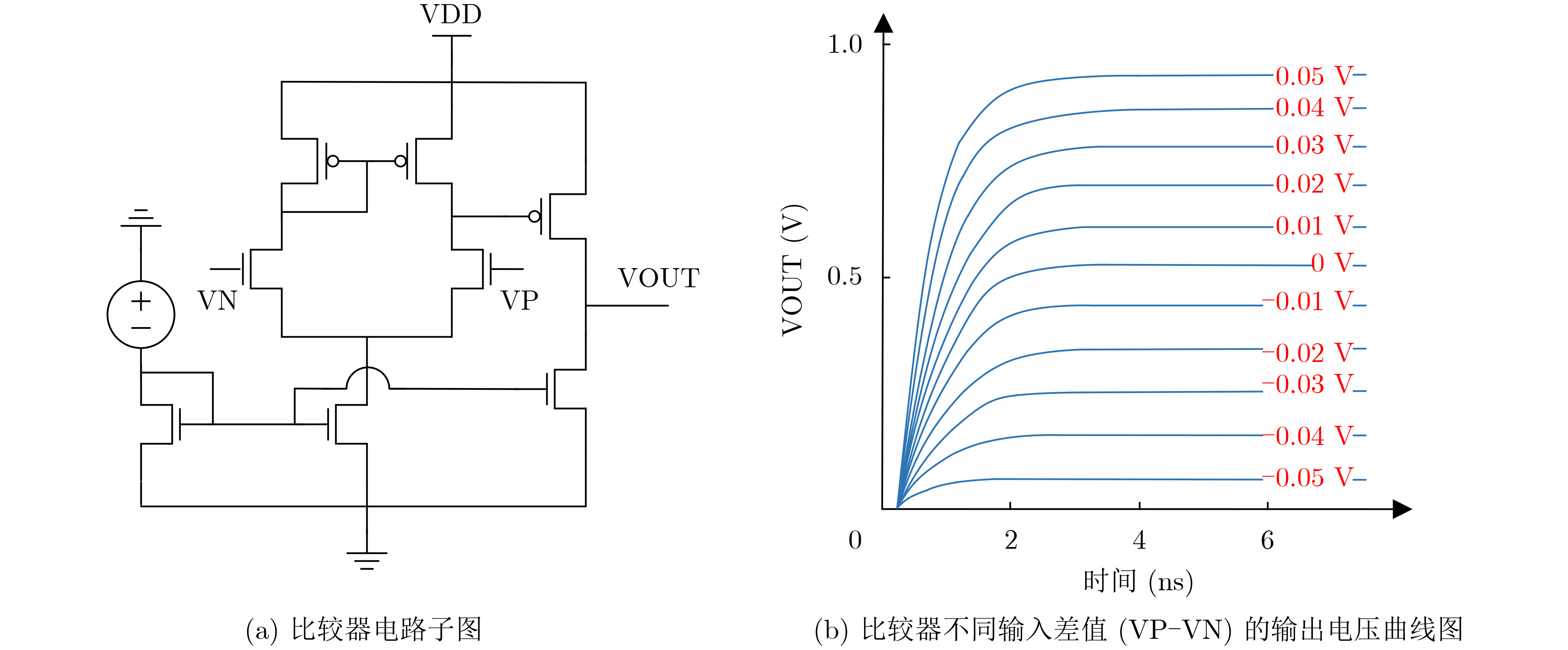
    Figures(3)  / Tables(4)

    Article Metrics

    Article views (83) PDF downloads(5) Cited by()
    Proportional views
    Related

    /

    DownLoad:  Full-Size Img  PowerPoint
    Return
    Return