




3-D Design Space Exploration of NTT/INTT Hardware Accelerators for ML-KEM and ML-DSA
-
摘要: 量子计算的发展对传统公钥密码构成严重威胁,后量子密码(PQC)成为安全领域的研究热点。基于模格的密钥封装机制(ML-KEM)与基于模格的数字签名算法(ML-DSA,Module-Lattice-Based Digital Signature Algorithm)作为美国国家标准与技术研究院(NIST)选定的标准化算法,其核心的多项式乘法运算采用数论变换(Number Theoretic Transform, NTT)实现,而NTT/INTT(Inverse NTT,INTT)硬件加速器的效率直接影响系统实时性与功耗。为应对从资源受限到资源充裕等多样化应用场景对资源与性能的不同需求,以及在同一硬件平台上同时高效支持ML-KEM与ML-DSA的工程挑战,本文提出一种面向二者的可配置NTT/INTT硬件加速器设计方法。通过构建包含模乘单元实现策略(DSP密集型与LUT密集型)、存储器接口策略(双读单写与双读双写)及流水线策略的三维设计空间模型,量化各维度对资源、时序及综合指标的影响。基于FPGA(Field-Programmable Gate Array, FPGA)平台,实例化多个代表性设计配置并完成综合验证。实验结果表明:LUT密集型Barrett模乘单元较DSP密集型方案节省60%以上DSP资源,且在大位宽场景下延迟更低;双读双写存储器接口使NTT计算吞吐率提升1倍;四级流水线使ML-KEM与ML-DSA模乘关键路径延迟分别从17.252 ns降至4.052 ns、从15.114 ns降至4.359 ns,面积-延迟积分别下降73%与71%。在整体NTT/INTT加速器层面,四级流水线相比三级流水线使ML-KEM与ML-DSA的功耗分别降低4.8%与12.9%。最终收敛至最优配置:LUT密集型模乘、双读双写接口、四级流水线,该配置下ML-KEM与ML-DSA的NTT加速器面积-时间积分别为1.782 KLUT·μs与3.073 KLUT·μs。Abstract:
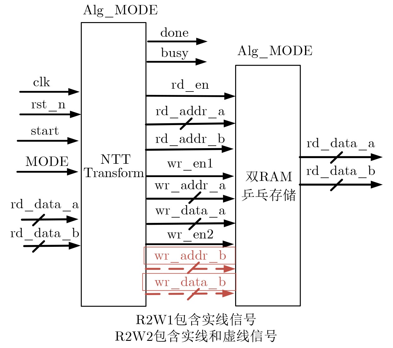
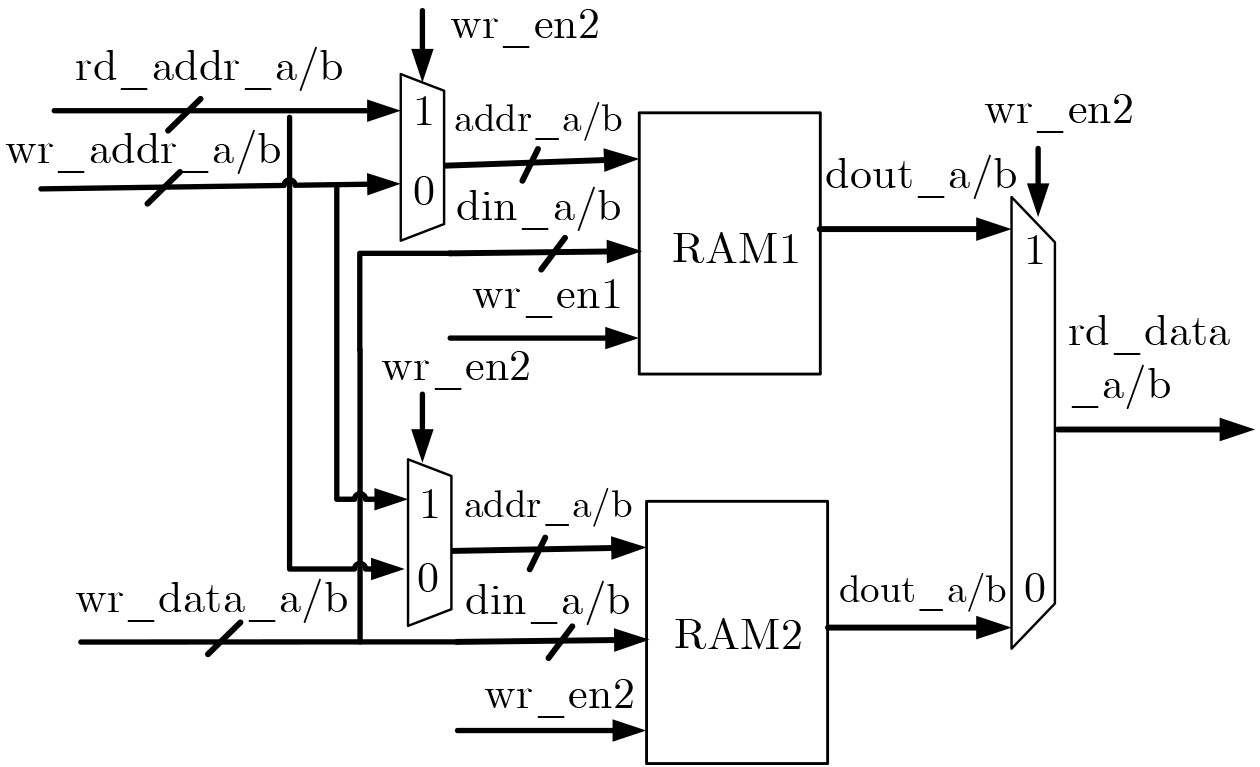
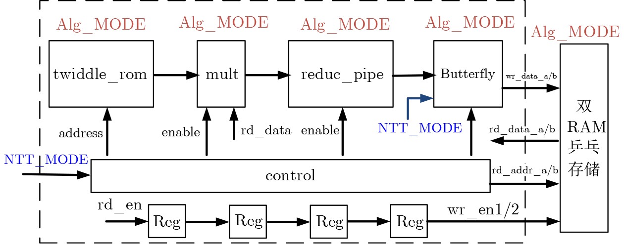
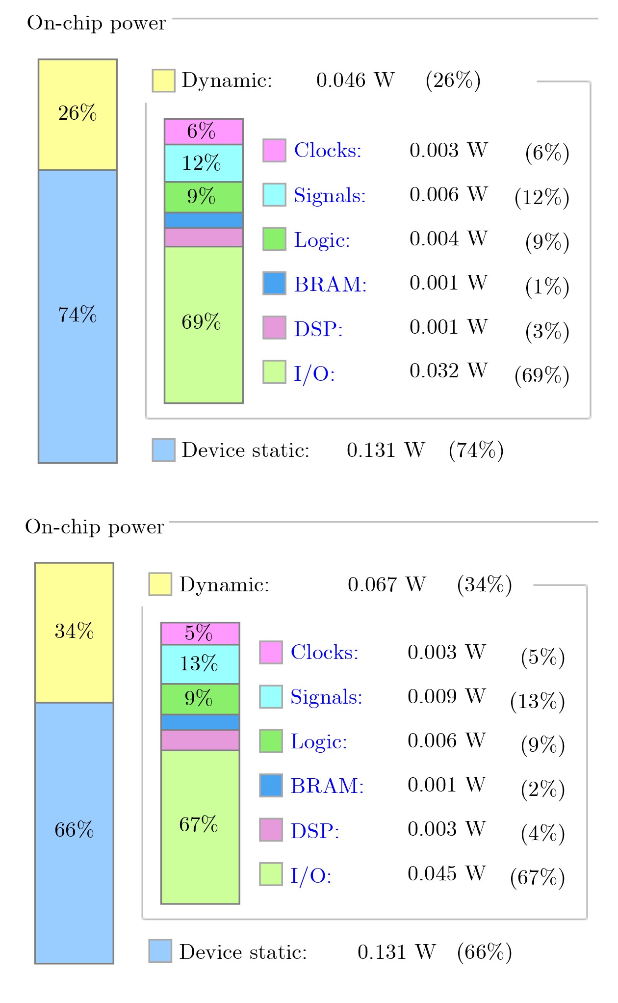
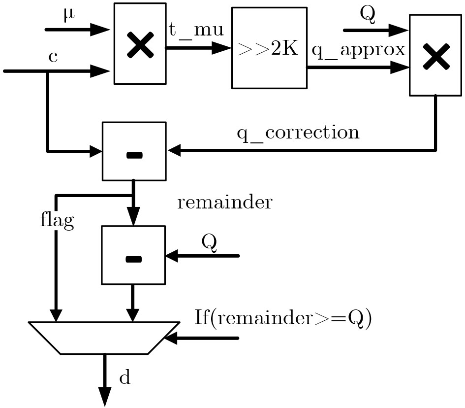
Objective The rapid development of quantum computing poses a serious threat to traditional public-key cryptosystems, making post-quantum cryptography (PQC) a critical research area. The module-lattice-based key-encapsulation mechanism (ML-KEM) and digital signature algorithm (ML-DSA), standardized by the National Institute of Standards and Technology (NIST), rely on polynomial multiplication using the number theoretic transform (NTT) and its inverse (INTT). The efficiency of NTT/INTT hardware accelerators directly impacts the real-time performance and power consumption of these algorithms. Diverse application scenarios, ranging from ranging from resource-constrained to resource-rich environments, demand different trade-offs between hardware resources and computational throughput. Furthermore, supporting both ML-KEM and ML-DSA efficiently on a single hardware platform poses a significant engineering challenge. To address these issues, this paper proposes a configurable NTT/INTT hardware accelerator design methodology that systematically explores the design space across three orthogonal dimensions. Methods The design space is modeled along three dimensions: modular multiplication implementation strategy (DSP-intensive vs. LUT-intensive), memory interface strategy (two-read-one-write vs. two-read-two-write), and pipeline depth (2-stage to 4-stage). For modular multiplication, two variants of the Barrett reduction are implemented. The DSP-intensive variant uses dedicated DSP slices for multiplication and accumulation, while the LUT-intensive variant uses only look-up tables and shift-add operations, consuming no DSP resources. For the memory interface, the two-read-two-write (R2W2) mode fully utilizes the dual-write-port capability of block RAM (BRAM) to eliminate write conflicts, achieving one butterfly operation per cycle. The two-read-one-write (R2W1) mode requires two write cycles per butterfly, reducing throughput by 50%. For pipelining, four pipeline stages are inserted into the LUT-intensive Barrett modular multiplier to shorten the critical path: stage 1 performs multiplication, stage 2 calculates the intermediate sum, stage 3 computes the difference, and stage 4 finalizes the reduction with a correction multiplexer. A “write-valid auto-delay” mechanism is designed to align write enables with the pipeline depth, simplifying control logic. The unified architecture supports algorithm configurability via an Alg_MODE parameter (selecting ML-KEM or ML-DSA) and dynamic NTT/INTT switching via an NTT_MODE signal. The proposed design is synthesized on a Xilinx Artix-7 FPGA (xc7a200t) using Vivado 2017.4 and ISE 14.4 for comparison.Results and Discussions Comprehensive evaluations are conducted on the modular multiplier, memory interface, pipeline stages, and the full NTT/INTT accelerator. For the modular multiplier ( Table 2 ), the LUT-intensive Barrett reduces equivalent LUT area (ELUT) by 55.3% for ML-KEM (from 928 to 415) and by 75.1% for ML-DSA (from3105 to 773) compared to the DSP-intensive version. The equivalent area-delay product (EAD) is reduced by 41.89% for ML-KEM and by 83.23% for ML-DSA, demonstrating superior resource efficiency, especially for large bit widths. For the memory interface (Table 3 ), the R2W2 mode achieves a 100% higher NTT throughput than R2W1, with slightly lower LUT and register counts due to simplified control logic. For pipeline optimization (Table 4 ), the 4-stage pipeline reduces the critical path delay of the ML-DSA modular multiplier from 15.114 ns to 4.359 ns (71% reduction) and that of ML-KEM from 17.252 ns to 4.052 ns (76.5% reduction). The area-delay product (ADP) drops by 73.4% for ML-KEM and 71.3% for ML-DSA. At the full accelerator level (Table 8 ), the 4-stage pipeline achieves an area-time product (ATP) of 1.782 KLUT·μs for ML-KEM and 3.073 KLUT·μs for ML-DSA. Compared to the 3-stage pipeline, the 4-stage pipeline reduces power consumption by 4.8% for ML-KEM and 12.9% for ML-DSA (Table 9 ). The power breakdown (Fig.5 ) shows that the modular reduction unit's power share drops from 47% (3-stage) to 38% (4-stage) for ML-DSA. Compared to state-of-the-art single-butterfly designs (Table 10 ), the proposed accelerator reduces ATP by 25.15% for ML-KEM and by 1.44% for ML-DSA, while using fewer LUTs and BRAMs.Conclusions This paper presents a systematic three-dimensional design space exploration method for configurable NTT/INTT hardware accelerators targeting ML-KEM and ML-DSA. By abstracting the design space into modular multiplication strategy, memory interface strategy, and pipeline depth, the quantitative trade-offs among resources (LUT, DSP, BRAM), timing (frequency, delay), and power are analyzed. The optimal configuration is converged to LUT-intensive Barrett modular multiplication, a two-read-two-write memory interface, and a 4-stage pipeline. Experimental results on FPGA demonstrate that this configuration achieves excellent balance between resource efficiency and performance, with ATP values of 1.782 KLUT·μs for ML-KEM and 3.073 KLUT·μs for ML-DSA. The proposed methodology can be extended to other NTT-based PQC algorithms and provides data-driven guidelines for flexible hardware accelerator design targeting both edge devices and cloud servers. Future work will explore efficient polynomial multiplication based on this NTT/INTT accelerator and extend the method to more domestic and international standardization algorithms. -
Key words:
- Post-quantum cryptography /
- Number theoretic transform (NTT) /
- Hardware acceleration /
- ML-KEM /
- ML-DSA
-
表 1 不同Alg_MODE模式下的全局常量
全局常量
全局参数ML-KEM:
Alg_MODE=1ML-DSA:
Alg_MODE=0模数Q 3329 8380417 Barrett约减常数μ 5039 8396807 约减常数μ的位宽K 24bit 46bit INTT归一化因子factor 3303 8347681 系数位宽DATA_WIDTH 12 bit 23 bit 乘积位宽PRODUCT_WIDTH 24bit 46bit NTT/INTT层数L 7 8  下载: 导出CSV
1 统一NTT算法(CT结构,与FIPS 203/204标准一致)
参数:Alg_MODE(1:ML-KEM, 0:ML-DSA) 输入:多项式系数数组$ f\in \mathbb{Z}_{q}^{256} $,预计算旋转因子 zetas[] 输出:NTT域系数数组$ \hat{f}\in \mathbb{Z}_{q}^{256} $ 算法步骤: 1.初始化数组和旋转因子索引:$ \hat{f}\leftarrow f,i\leftarrow 1 $, 2.for (len←128; len≥1+Alg_MODE; len←len/2) do // 外层循环 3. for (start←0; start<256; start←start+2len) do // 中层循环 4. $ zeta\leftarrow \text{zetas}[i] $//获取当前层的旋转因子 5. $ i\leftarrow i+1 $// 递增旋转因子索引 6. for (j←start; j<start+len; j++) do // 内层循环 7. $ t\leftarrow (zeta\cdot \hat{f}[j+len])\mathrm{mod} q $ 8. $ \hat{f}[j+len]\leftarrow \left(\hat{f}[j]-t\right)\mathrm{mod} q $ 9. $ \hat{f}[j]\leftarrow \left(\hat{f}[j]+t\right)\mathrm{mod} q $ 10.return f //返回NTT变换后的频域多项式系数
下载: 导出CSV
2 统一INTT算法(GS结构,与FIPS 203/204标准一致)
参数:Alg_MODE(1:ML-KEM, 0:ML-DSA) 输入:NTT域系数数组$ \hat{f}\in \mathbb{Z}_{q}^{256} $,预计算旋转因子 zetas[] 输出:时域多项式系数数组$ f\in \mathbb{Z}_{q}^{256} $ 算法步骤: 1.初始化数组:$ f\leftarrow \hat{f} $,初始化旋转因子索引:
$ i\leftarrow 127\left(\text{Alg}\_\text{MODE}=1\right)或255\left(\text{Alg}\_\text{MODE}=0\right) $2.for (len←1+Alg_MODE; len≤ 128; len←2len) do//外层循环 3 .for (start←0; start<256; start←start+2len) do//中层循环 4. $ zeta\leftarrow \text{zetas}[i] $// 获取当前层的旋转因子 5. $ i\leftarrow i-1 $// 递减旋转因子索引,从后向前遍历 6. for (j←start; j<start+len; j++) do // 内层循环 7. $ t\leftarrow \left(f[j+\text{len}]-f[j]\right)\mathrm{mod} q $ 8. $ f[j]\leftarrow (f[j]+f[j+len])\mathrm{mod} q $ 9. $ f[j+\text{len}]\leftarrow \text{zeta}\cdot t\mathrm{mod} q $ 10.for j←0; j<256; j←j++ do//归一化处理 11. $ f[j]\leftarrow (f[j]\cdot \text{factor})\mathrm{mod} q $ 12.return f //返回INTT变换后的时域多项式系数
下载: 导出CSV
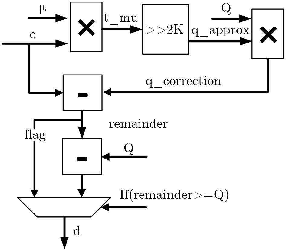
3 Barrett模约减算法
参数:Alg_MODE(1:ML-KEM, 0:ML-DSA) 输入:整数c(0≤c≤(Q-1)2),位宽为 2×DATA_WIDTH 输出:result=c modQ 算法步骤: 1.t_mu←c×μ //计算中间值,位宽为3×DATA_WIDTH+1 2.q_approx←t_mu>> K//计算近似商,位宽
2×DATA_WIDTH3.q_correction←q_approx×Q/计算修正项,位宽为
2×DATA_WIDTH4.remainder←c−q_correction //计算临时余数,位宽
DATA_WIDTH+15.if remainder≥Q then corrected←remainder−Q else corrected←remainder//余数修正 6.result←corrected // 返回结果,位宽DATA_WIDTH
下载: 导出CSV
4 LUT密集型Barrett模约减算法
参数:Alg_MODE(1: ML-KEM, 0: ML-DSA) 输入:c (ML-KEM: 24 bits, ML-DSA: 46 bits)//整数c 输出:d ≡ c mod Q (Q = 3329 或8380417 )//模约减后值d局部参数: C1_WIDTH = Alg_MODE ? 14 : 33;C2_WIDTH = Alg_MODE ? 18 : 43;C3_WIDTH = 20;算法步骤: 1.分段提取 1.1 c0 ← c[PRODUCT_WIDTH-1:DATA_WIDTH] 1.2 c1 ← c[PRODUCT_WIDTH-1:C1_WIDTH] 1.3 c2 ← c[PRODUCT_WIDTH-1:C2_WIDTH] 1.4 c3 ← c[PRODUCT_WIDTH-1:C3_WIDTH] 2.准确计算μ*c,近似计算q_approx 2.1如果 Alg_MODE = 1: sum ← c0 + c1 - c2 - c3 t ← sum + (sum[6:0] << 8) + (sum[4:0] << 10) +
(sum[3:0] << 11)2.2否则: sum ← c0 + c1 + c2 t ← sum + (sum[2:0] << 23) - (sum[12:0] << 13) 3.差值计算:diff ← c[DATA_WIDTH+2:0] - t 4.标志位提取:flag← diff[DATA_WIDTH+2:DATA_WIDTH] 5.结果修正 5.1如果 Alg_MODE = 1: 根据 flag 选择 p_mux: 0: 0x0 1: 0x72FF //-q 5,6: 0x2703 //+3q 7: 0x1A02 //+2q 否则: 根据 flag 选择 p_mux: 0: 0x0 1: 0x3801FFF//-q 2: 0x3003FFE//-2q 3: 0x2805FFD//-3q 5,6: 0x17FA003//+3q 7: 0x0FFC002//+2q 6.修正与最终约减 6.1 diff2 ← diff + p_mux 6.2 diff2p ← diff2 - Q 6.3 如果 diff2p[DATA_WIDTH] = 1 // 检查符号位 d ← diff2[DATA_WIDTH-1:0] 否则: d ← diff2p[DATA_WIDTH-1:0] 7.return d
下载: 导出CSV
表 2 流水线各阶段功能划分
流水线 一级 二级 三级 四级 无 乘法+模约减 二级 乘法 模约减 - - 三级 乘法 算出t 算出diff2 - 四级 乘法 算出sum 算出diff 算出d
下载: 导出CSV
表 3 Artix7 XC7A200T FBG484 -2 FPGA平台资源
平台资源 Reg LUT LUT RAM BRAM DSP xc7a200t 269200 134600 46200 365 750
下载: 导出CSV
表 4 基于Barrett摸约减的模乘结果
类型 Alg LUT DSP Delays ELUT EADP DSP密集 ML-KEM 28 3 13.278 928 12.322 ML-DSA 105 10 22.440 3105 69.676 LUT密集 ML-KEM 115 1 17.252 415 7.160
↓41.89%ML-DSA 173 2 15.114 773 11.683
↓83.23%
下载: 导出CSV
表 5 ISE综合结果接口策略对比
算法 接口 Reg LUT BRAM DSP Delays ADP ML-KEM R2W1 81 632 1 1 18.180 11.490 R2W2 61 617 1 1 18.180 11.217 ML-DSA R2W1 114 970 1 2 19.768 19.175 R2W2 83 944 1 2 19.768 18.661
下载: 导出CSV
表 6 ISE流水线综合结果
算法 级数 Reg LUT DSP Delays ADP ML-KEM 无 — 115 1 17.252 1.984 二级 42 110 1 6.602 0.726 三级 30 130 1 6.336 0.824 四级 44 130 1 4.052 0.527 ML-DSA 无 — 173 2 15.114 2.615 二级 77 172 2 7.942 1.366 三级 69 172 2 5.999 1.032 四级 97 172 2 4.359 0.750
下载: 导出CSV
表 7 三级流水NTT加速器的ISE综合结果对比
Alg FF LUT LUT
RAMBRAM DSP 时延 周期数 ATP ML-KEM 167 519 41 1 1 5.843 902 2.735 ML-DSA 261 741 63 1 2 5.491 1030 4.190
下载: 导出CSV
表 9 四级流水NTT加速器的ISE综合结果对比
Alg FF LUT LUT
RAMBRAM DSP 时延 周期数 ATP ML-KEM 180 487 40 1 1 4.523 902 1.987 ML-DSA 285 734 62 1 2 5.491 1030 4.151
下载: 导出CSV
表 8 三级流水NTT加速器的Vivado默认综合结果对比
Alg FF LUT LUT
RAMBRAM DSP 时延 周期数 ATP ML-KEM 172 379 41 0.5 1 6.027 902 2.060 ML-DSA 266 589 63 0.5 2 5.217 1030 3.165 注:LUTRAM为LUT作为分布式RAM使用;BRAM计为0.5表示使用1个18Kb BRAM。
下载: 导出CSV
表 10 四级流水NTT加速器Vivado默认综合结果对比
Alg FF LUT LUT
RAMBRAM DSP 时延 周期数 ATP ML-KEM 187 379 40 0.5 1 5.207 903 1.782 ML-DSA 292 572 62 0.5 2 5.210 1031 3.073
下载: 导出CSV
表 12 NTT/INTT实现的Vivado综合的结果比较
a)单并行蝶形架构对比 参考文献 Alg Butterfly Cycles LUT FF Delays/ns Time/us BRAM DSP ATP/KLUT·μs 器件 本文
(四级流水)ML-DSA 1并行 1031 572 292 5.210 5.372 0.5 2 3.073 Artix-7 文献[20] ML-DSA 1并行 654 2379 2219 2.801 1.83 4 16 9.48(基4) Virtex-7 文献[19] ML-DSA 1并行 1691 6522 3018 5.920 10.01 5. 48 158.56 Virtex-7 文献[16] ML-DSA 1并行 1295 732 722 4.17 5.4 1 4 3.953 Artix-7 文献[8] ML-DSA 1并行 1031 655 213 4.618 4.76 1 1 3.118 Artix-7 本文
(四级流水)ML-KEM 1并行 903 379 187 5.207 4.702 0.5 1 1.782 Artix-7 文献[19] ML-KEM 1并行 859 6522 3018 5.915 5.08 5 48 80.47 Virtex-7 文献[15] ML-KEM 1并行 904 948 352 5.263 4.767 2.5 1 4.519 Artix-7 文献[8] ML-KEM 1并行 903 655 213 4.618 4.17 1 1 2.731 Artix-7 文献[17] ML-KEM 1并行 2310 1778 33 14.286 3.30 0 5 5.867. Artix-7 b)多并行蝶形架构对比 参考文献 Alg Butterfly Cycles LUT FF Delay/ns Times/us BRAM DSP ATP(KLUT·μs) 器件 文献[8] ML-DSA 4并行 263 1688 672 5.81 1.30 4 4 2.194 Artix-7 文献[9] ML-DSA 8并行 128 7451 5275 5.556 0.711 0 0 5.298 Artix-7 文献[18] ML-DSA 8并行 286 4187 4387 3.367 0.96 0 18 4.020 Artix-7 文献[14] ML-KEM 2并行 456 1154 21031 3.33 1.52 0 2 15.984 Artix-7 文献[8] ML-KEM 4并行 263 1688 672 5.81 1.14 4 4 1.924 Artix-7 文献[13] ML-KEM 4并行 251 912 260 4.00 1.00 16 0 0.9 Artix-7 文献[9] ML-KEM 4并行 277 4834 4683 4.00 1.11 1 0 5.366 Artix-7
下载: 导出CSV
-
[1] MOODY D, PERLNER R, REGENSCHEID A, et al. Transition to post-quantum cryptography standards: Initial public draft[R]. NIST Internal Report NIST IR 8547 ipd, 2024. [2] SCHWABE P, AVANZI R. J, BOS J, et al. Crystals-kyber[C]. NIST Post-Quantum Cryptography Standardization Round 3 Submissions, Gaithersburg, USA, 2022. (查阅网上资料, 未找到本条文献信息, 请确认). [3] LYUBASHEVSKY V, DUCAS L, KILTZ E, et al. Crystals-dilithium[C]. NIST Post-Quantum Cryptography Standardization Round 3 Submissions, Gaithersburg, USA, 2022. (查阅网上资料, 未找到本条文献信息, 请确认). [4] National Institute of Standards and Technology. FIPS 203 Module-lattice-based key-encapsulation mechanism standard[S]. Washington: U. S. Department of Commerce, 2024. doi: 10.6028/NIST.FIPS.203. [5] National Institute of Standards and Technology. FIPS 204 Module-lattice-based digital signature standard[S]. Washington: U. S. Department of Commerce, 2024. doi: 10.6028/NIST.FIPS.204. [6] 刘冬生, 邹雪城, 张聪, 等. 后量子密码芯片设计[M]. 北京: 电子工业出版社, 2023. (查阅网上资料, 未找到页码信息, 请确认补充).LIU Dongsheng, ZOU Xuecheng, ZHANG Cong, et al. Chip Design for Post-Quantum Cryptography[M]. Beijing: Publishing House of Electronics Industry, 2023. [7] XING Yufei and LI Shuguo. An efficient implementation of the NewHope key exchange on FPGAs[J]. IEEE Transactions on Circuits and Systems I: Regular Papers, 2020, 67(3): 866–878. doi: 10.1109/TCSI.2019.2956651. [8] 赵旭阳, 梁志闯, 胡跃, 等. NTT架构研究及其FPGA硬件优化实现[J]. 计算机学报, 2023, 46(12): 2670–2686. doi: 10.11897/SP.J.1016.2023.02670.ZHAO Xuyang, LIANG Zhichuang, HU Yue, et al. NTT architecture research and its FPGA hardware optimization implementation[J]. Chinese Journal of Computers, 2023, 46(12): 2670–2686. doi: 10.11897/SP.J.1016.2023.02670. [9] NGUYEN T H, KIEU-DO-NGUYEN B, PHAM C, et al. High-speed NTT accelerator for CRYSTAL-Kyber and CRYSTAL-Dilithium[J]. IEEE Access, 2024, 12: 34918–34930. doi: 10.1109/ACCESS.2024.3371581. [10] BANERJEE U, UKYAB T S, and CHANDRAKASAN A P. Sapphire: A configurable crypto-processor for post-quantum lattice-based protocols[J]. IACR Transactions on Cryptographic Hardware and Embedded Systems, 2019, 2019(4): 17–61. doi: 10.46586/tches.v2019.i4.17-61. [11] MANDAL S and ROY D B. KiD: A hardware design framework targeting unified NTT multiplication for CRYSTALS-Kyber and CRYSTALS-Dilithium on FPGA[C]. 2024 37th International Conference on VLSI Design and 2024 23rd International Conference on Embedded Systems (VLSID), Kolkata, India, 2024: 455–460. doi: 10.1109/VLSID60093.2024.00082. [12] LU Jiahao, ZHANG Jiaming, LUO Zhixiang, et al. An efficient and configurable hardware architecture of polynomial modular operation for CRYSTALS-Kyber and Dilithium[C]. 2024 IEEE 67th International Midwest Symposium on Circuits and Systems (MWSCAS), Springfield, USA, 2024: 29–32. doi: 10.1109/MWSCAS60917.2024.10658892. [13] SALARIFARD R and SOLEIMANY H. An efficient hardware accelerator for NTT-based polynomial multiplication using FPGA[J]. Journal of Cryptographic Engineering, 2024, 14(2): 415–426. doi: 10.1007/s13389-024-00357-1. [14] NI Ziying, KHALID A, LIU Weiqiang, et al. Towards a lightweight CRYSTALS-Kyber in FPGAs: An ultra-lightweight BRAM-free NTT core[C]. IEEE International Symposium on Circuits and Systems (ISCAS 2023), Monterey, USA, 2023: 1–5. doi: 10.1109/ISCAS46773.2023.10181340. [15] YAMAN F, MERT A C, ÖZTÜRK E, et al. A hardware accelerator for polynomial multiplication operation of CRYSTALS-KYBER PQC scheme[C]. 2021 Design, Automation & Test in Europe Conference & Exhibition (DATE), Grenoble, France, 2021: 1020–1025. doi: 10.23919/DATE51398.2021.9474139. [16] ZHAO Yanrui, LIU Xiaofan, HU Yue, et al. Design of an efficient NTT/INTT architecture with low-complex memory mapping scheme[J]. IEEE Transactions on Circuits and Systems II: Express Briefs, 2024, 71(1): 400–404. doi: 10.1109/TCSII.2023.3296492. [17] ZHAO Yinqiao, XIE Zilong, ZHAN Ruidian, et al. NTT-LSU: Tightly coupled architecture for efficient NTT implementation on RISC-V processor[J]. IEEE Transactions on Computer-Aided Design of Integrated Circuits and Systems, 45(6): 2952–2961. doi: 10.1109/TCAD.2025.3627145. [18] CUI Yijun, ZHONG Junjie, WANG Bei, et al. High-performance hardware implementation of crystals-dilithium based on improved MDC-NTT[J]. IEEE Transactions on Computers, 2025, 74(9): 2896–2908. doi: 10.1109/TC.2025.3576934. [19] 陈韬, 赵旺鹏, 别梦妮, 等. 格基后量子密码双域可重构多项式乘法运算单元架构研究[J]. 电子与信息学报, 2026, 48(4): 1646–1658. doi: 10.11999/JEIT250929.CHEN Tao, ZHAO Wangpeng, BIE Mengni, et al. Research on the architecture of dual-field reconfigurable polynomial multiplication unit for lattice-based post-quantum cryptography[J]. Journal of Electronics & Information Technology, 2026, 48(4): 1646–1658. doi: 10.11999/JEIT250929. [20] 郑集文, 赵石磊, 张子悦, 等. 面向格密码的高面积效率基-4快速数论变换硬件架构与无访存冲突优化设计[J]. 电子与信息学报, 2026, 48(2): 855–865. doi: 10.11999/JEIT250687.ZHENG Jiwen, ZHAO Shilei, ZHANG Ziyue, et al. High area-efficiency radix-4 number theoretic transform hardware architecture with conflict-free memory access optimization for lattice-based cryptography[J]. Journal of Electronics & Information Technology, 2026, 48(2): 855–865. doi: 10.11999/JEIT250687. [21] 赵毅强, 孔金笛, 付玉成, 等. 面向模块化格基密钥封装机制算法多项式乘法的侧信道安全防护关键技术研究[J]. 电子与信息学报, 2025, 47(9): 3126–3136. doi: 10.11999/JEIT250292.ZHAO Yiqiang, KONG Jindi, FU Yucheng, et al. Research on key technologies of side-channel security protection for polynomial multiplication in ML-KEM/Kyber algorithm[J]. Journal of Electronics & Information Technology, 2025, 47(9): 3126–3136. doi: 10.11999/JEIT250292. -

 下载:
下载:

计量
- 文章访问数: 168
- HTML全文浏览量: 32
- PDF下载量: 8
- 被引次数: 0
