




A Novel TDMOSFET and Its Neural Network Modeling for Ternary Logic Applications
-
摘要: 目前三值逻辑电路设计面临所需器件多、涉及无源元件以及与传统互补金属氧化物半导体(CMOS)工艺兼容性差等诸多挑战。对此,该文提出一种基于量子隧穿与漂移扩散机制相结合的新型隧穿-漂移扩散场效应晶体管(TDMOSFET),该器件具有常数关态电流特性,适合于三值逻辑电路。该文分析了TDMOSFET工作原理,采用人工神经网络(ANN)对其建模,所建立ANN模型可以精确模拟器件电流-电压和电容-电压特性,预测精度高达99%。此外,将ANN模型转换为Verilog-A语言,嵌入到HSPICE工具中,仿真了基于TDMOSFET的标准三值反相器(STI)、负三值反相器(NTI)、正三值反相器(PTI)、三值与非门(T-NAND)及三值或非门(T-NOR)等基本单元电路,这些电路不涉及无源元件,可兼容于CMOS工艺,对于后续三值逻辑的研究具有重要参考意义。Abstract:
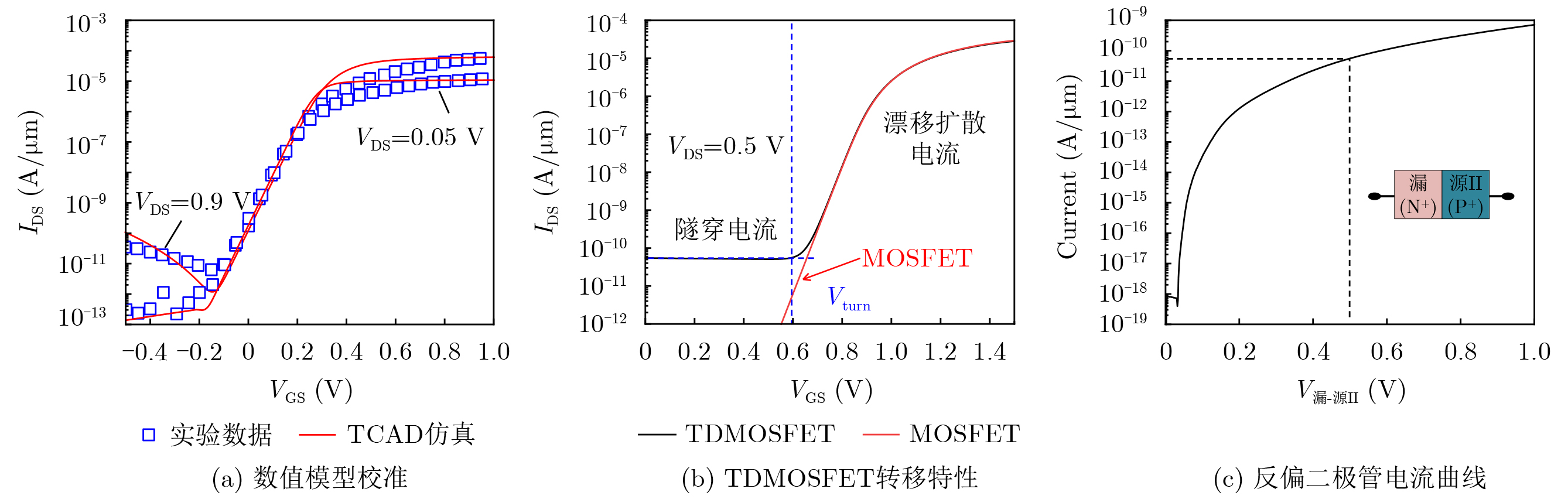
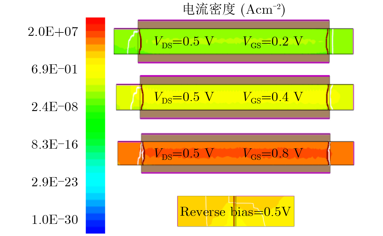
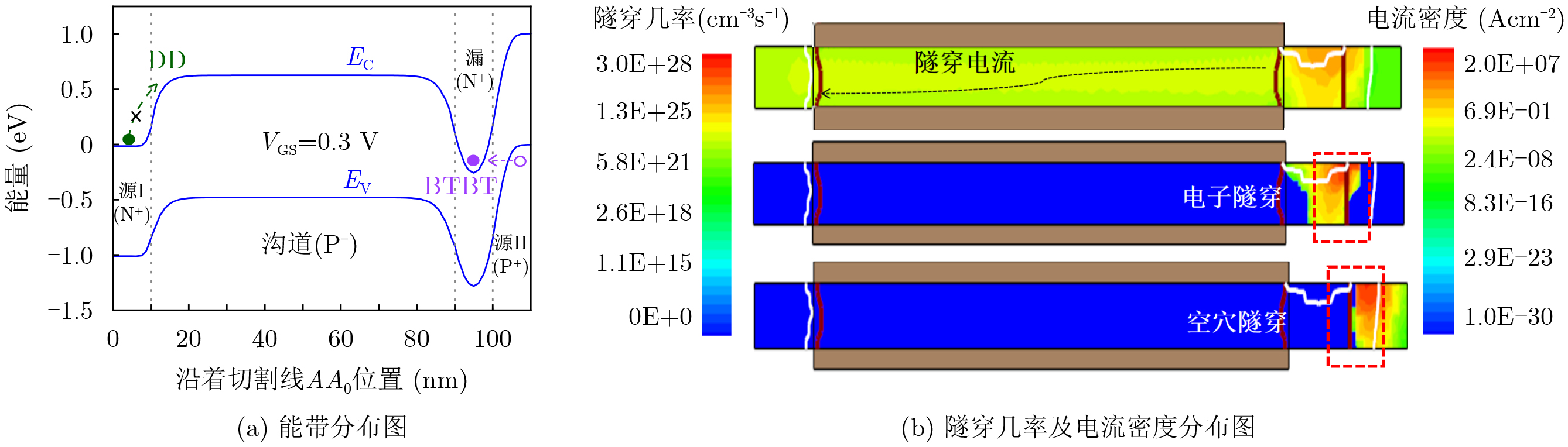
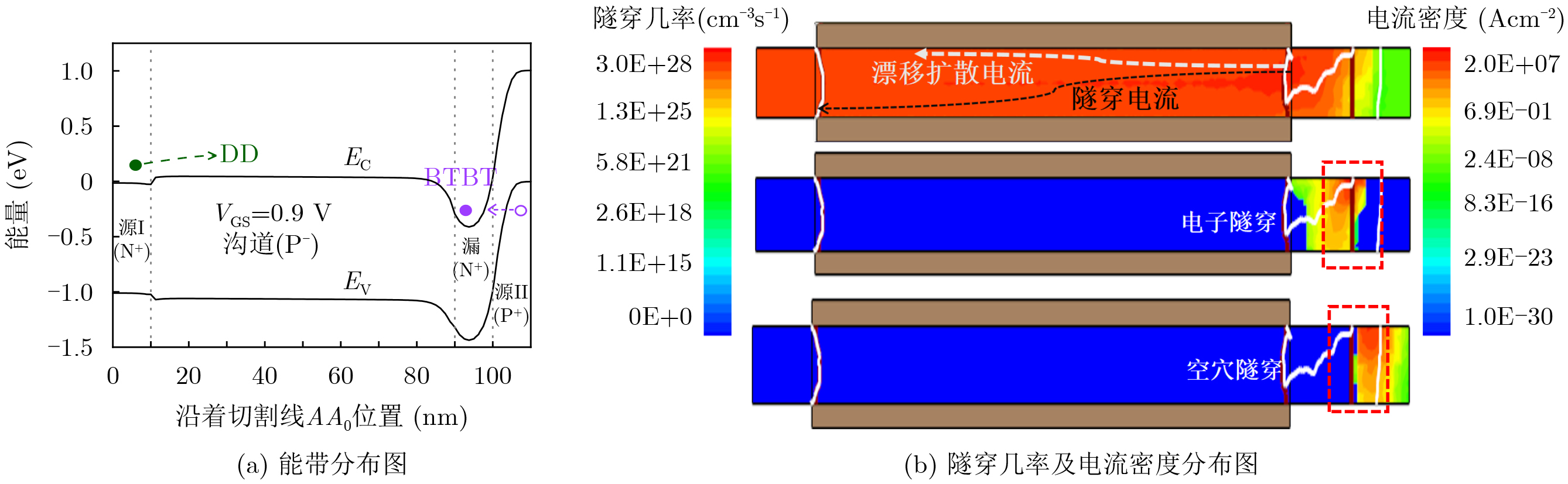
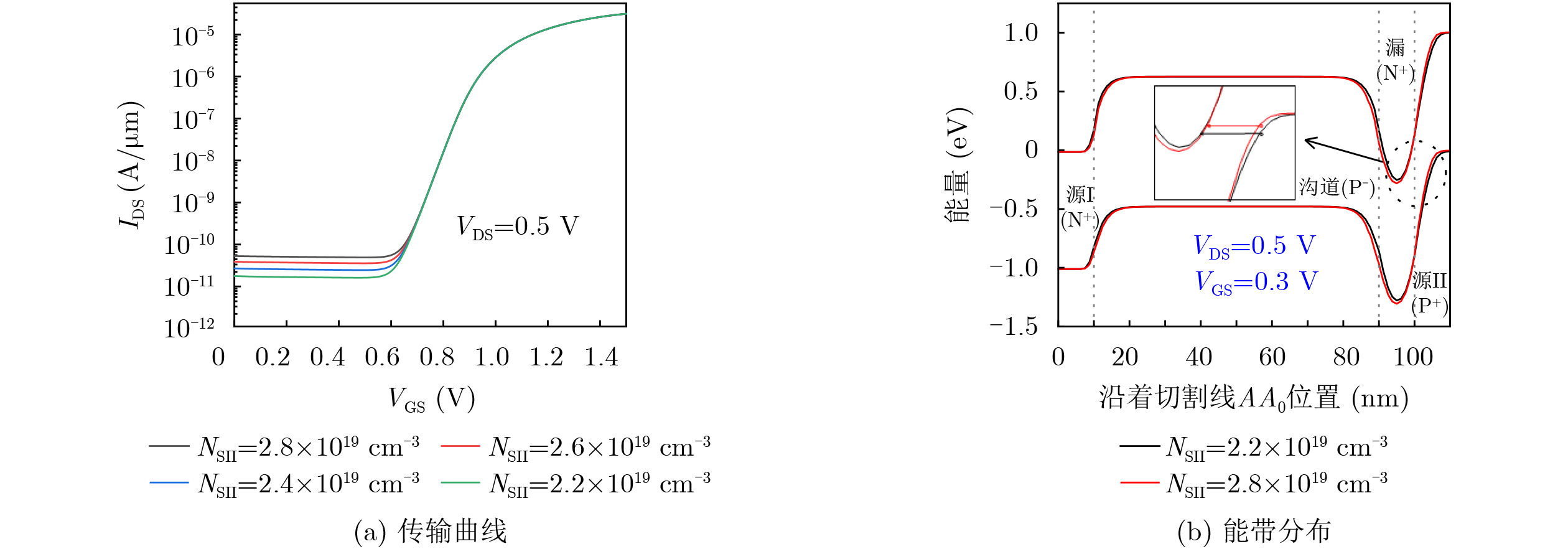
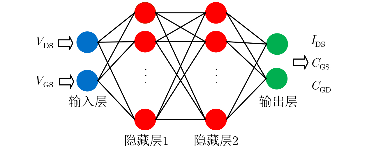
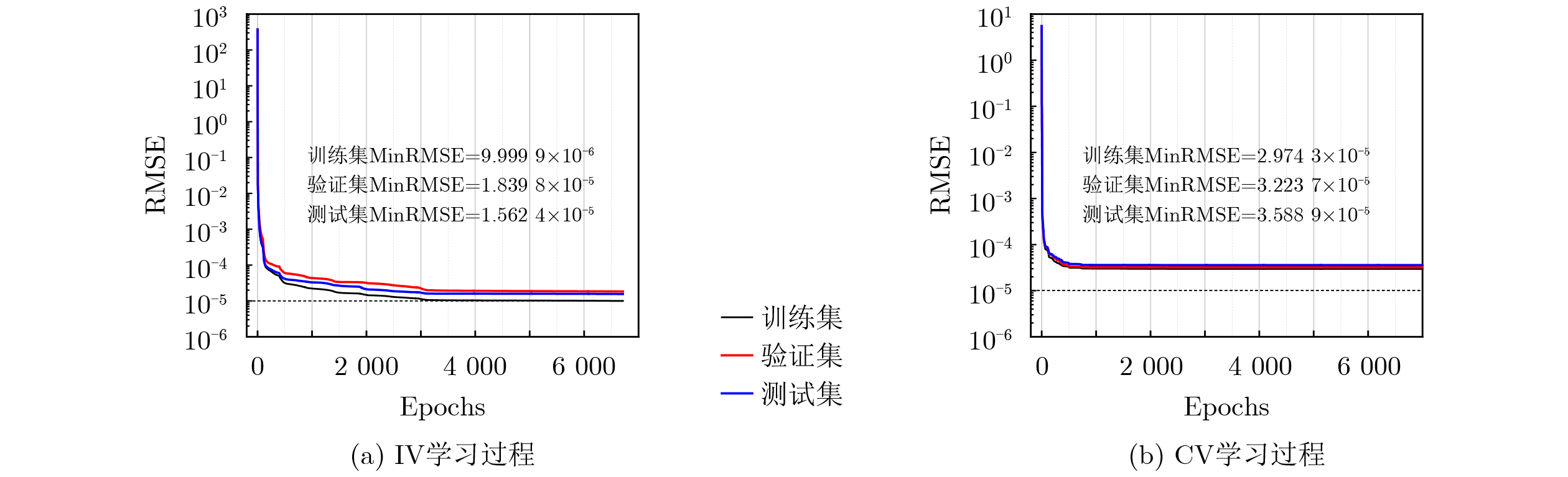
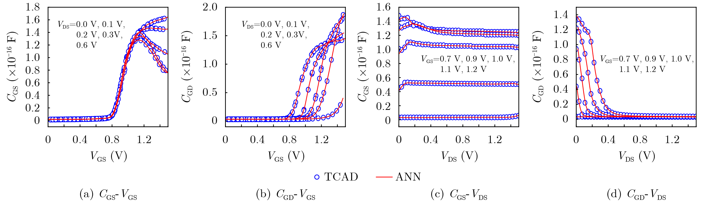
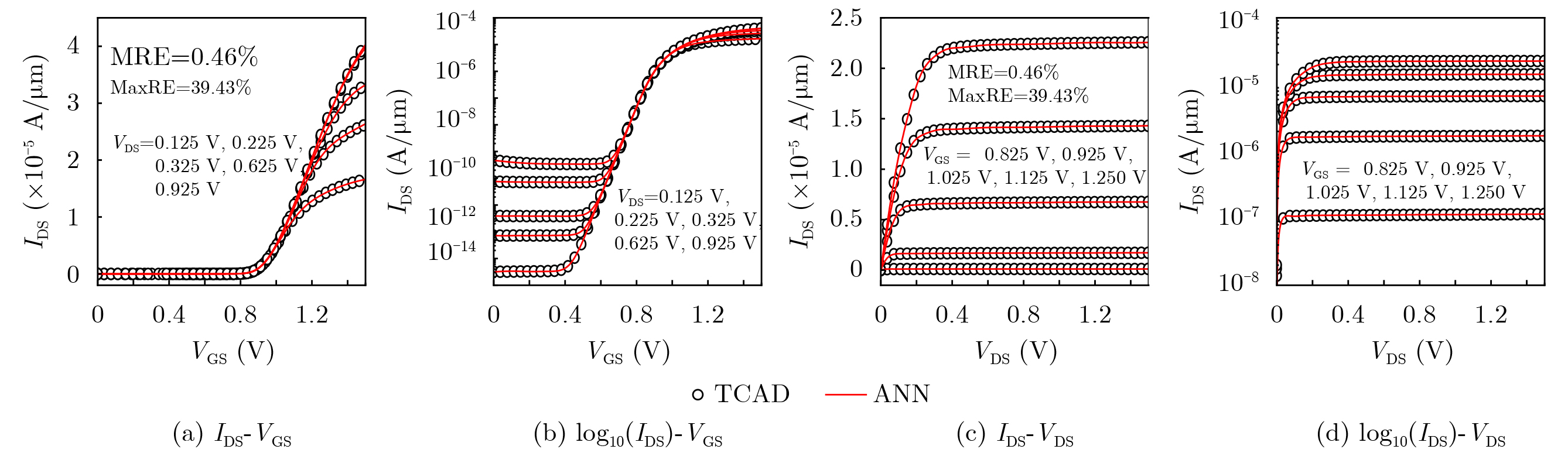
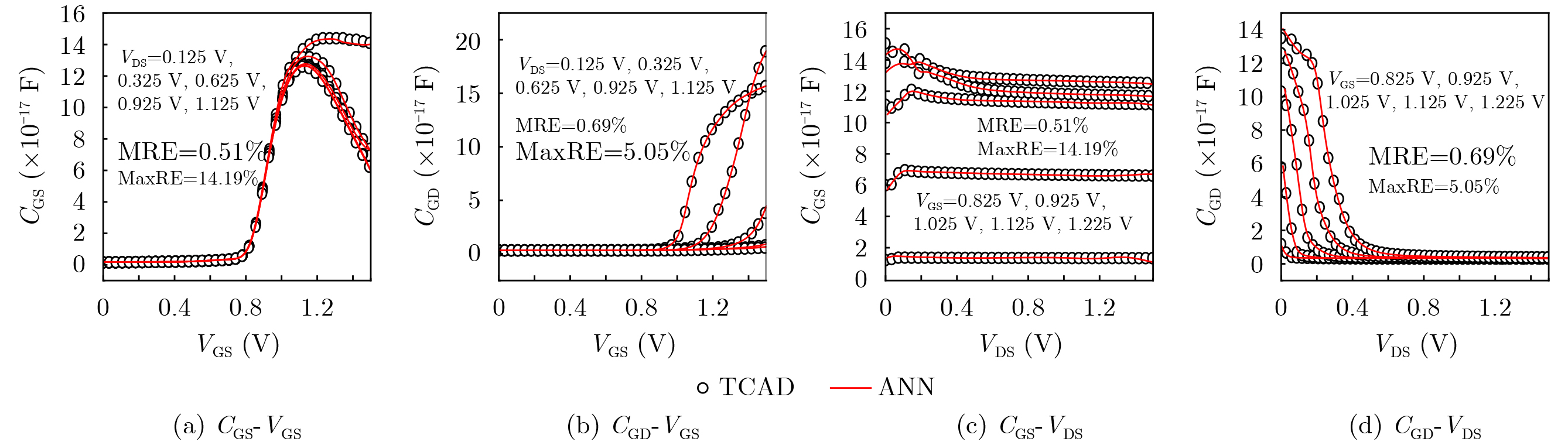
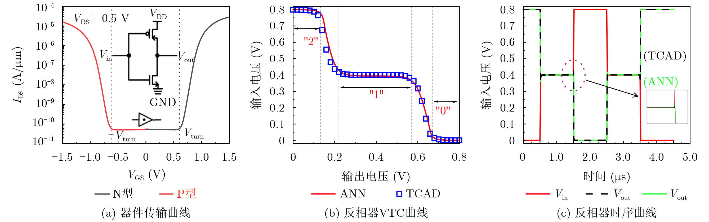
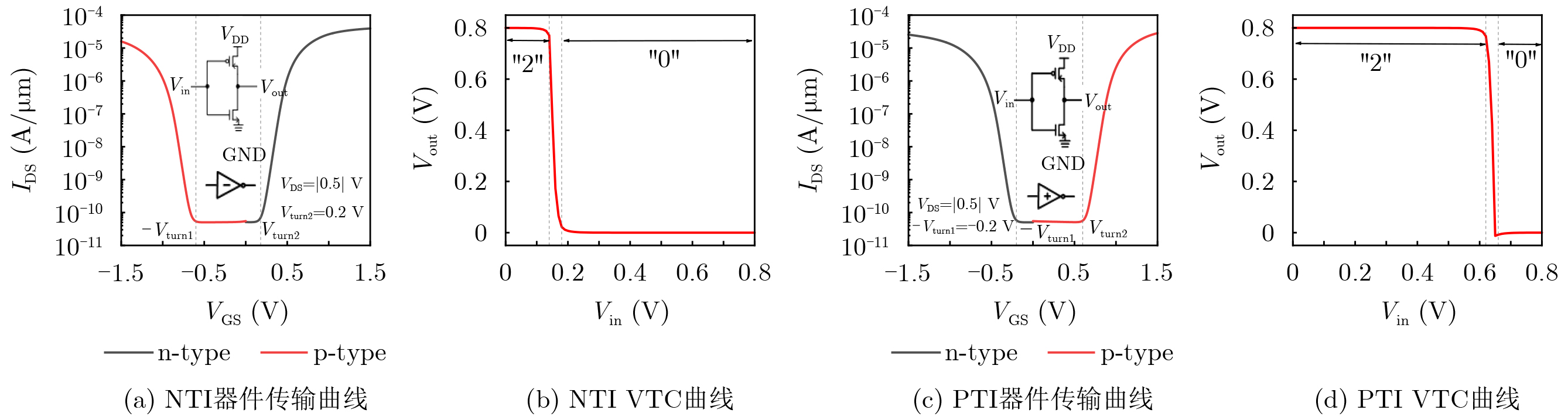
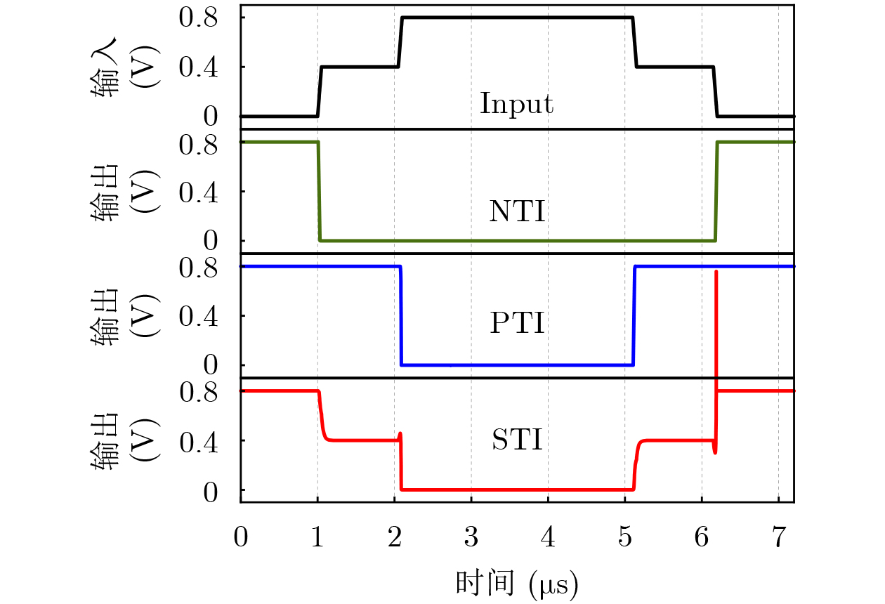
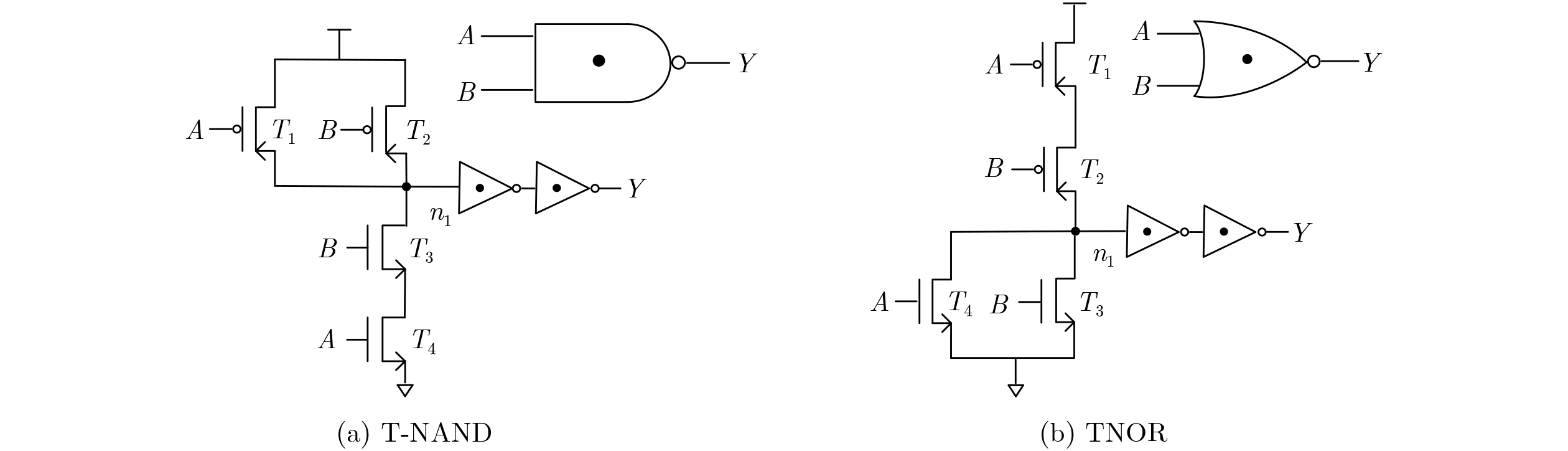
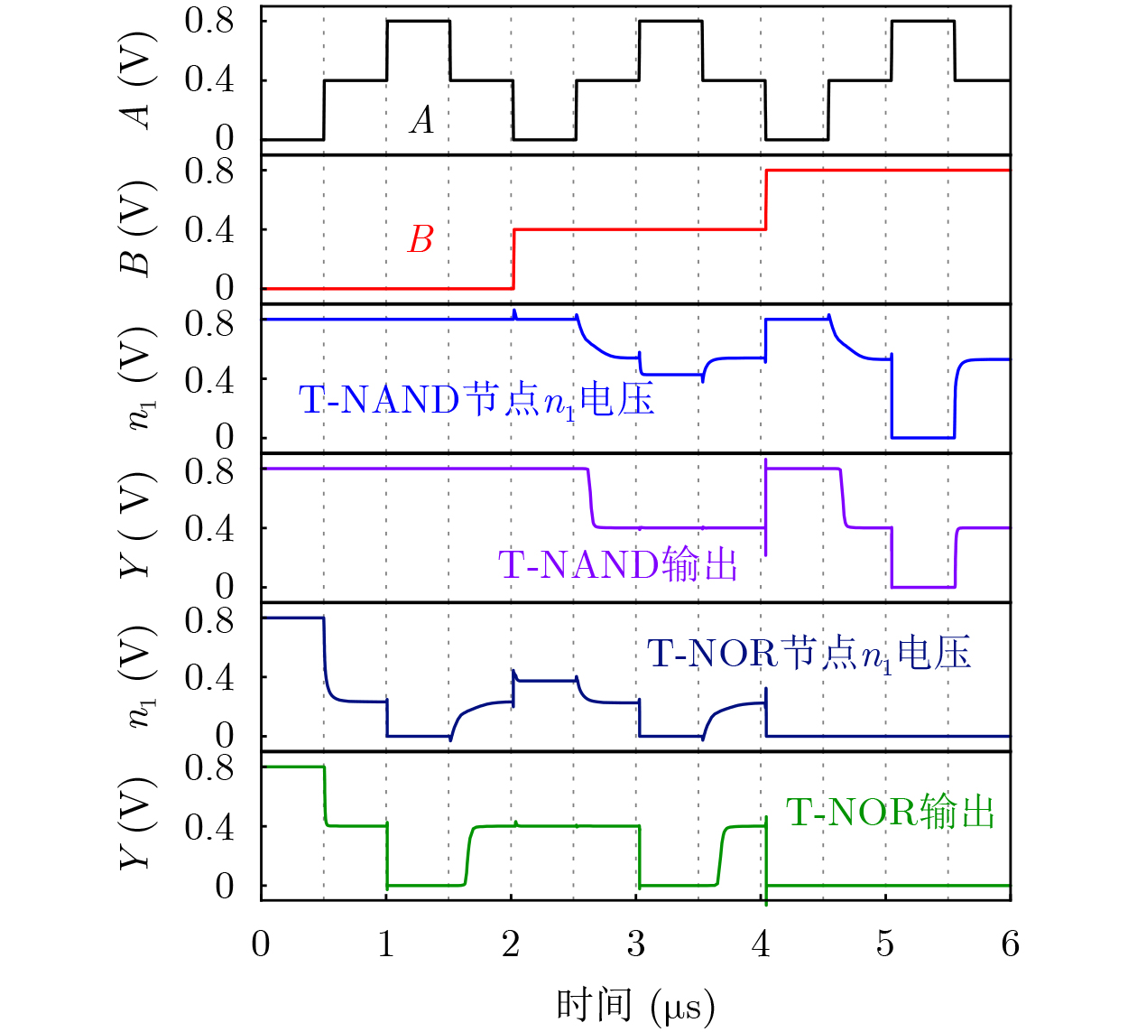
Objective Complementary Metal-Oxide-Semiconductor (CMOS) technology continues to advance toward smaller device dimensions and higher integration. As circuit integration increases, short-channel effects and other phenomena increase leakage current in MOSFET devices, resulting in higher static power consumption. With the rapid development of artificial intelligence, traditional binary logic faces limitations in processing and storing massive amounts of data. Ternary logic has therefore attracted increasing attention because it provides higher information density and lower system complexity than binary logic. However, current ternary logic circuits still face challenges, including the use of multiple components, passive elements, and poor compatibility with conventional CMOS processes. Methods A novel Tunneling-Drift-Diffusion Metal-Oxide-Semiconductor Field-Effect Transistor (TDMOSFET) that combines quantum tunneling and drift-diffusion mechanisms is proposed. The device exhibits a constant off-state current characteristic, making it suitable for ternary logic applications. Its operating principle is analyzed, and an Artificial Neural Network (ANN) is used to model its electrical characteristics. The ANN model is trained using Technology Computer-Aided Design (TCAD) simulation data to predict the current-voltage (I-V) and capacitance-voltage (C-V) characteristics. The trained ANN model is further converted into a Verilog-A model and integrated into HSPICE to simulate basic ternary logic circuits, including the Standard Ternary Inverter (STI), Negative Ternary Inverter (NTI), Positive Ternary Inverter (PTI), Ternary NOT-AND gate (T-NAND), and Ternary NOT-OR gate (T-NOR). Results and Discussions The trained ANN model accurately predicts the I-V and C-V characteristics of the TDMOSFET. Compared with the TCAD results, the maximum relative errors for the drain current (IDS), gate-drain capacitance (CGD), and gate-source capacitance (CGS) are 39.43%, 5.05%, and 14.19%, respectively, whereas the corresponding average relative errors are 0.46%, 0.69%, and 0.51%. The ANN model is successfully converted into a Verilog-A model and integrated into HSPICE for circuit-level simulation. The STI, NTI, PTI, T-NAND, and T-NOR circuits are successfully simulated. The TDMOSFET-based ternary logic circuits do not require passive elements and are compatible with conventional CMOS processes. Conclusions A novel TDMOSFET with dual conduction mechanisms is proposed. When the gate-source voltage is below the turning voltage (Vturn), band-to-band tunneling is the dominant conduction mechanism, and the device operates similarly to a reverse-biased tunneling diode. When the gate-source voltage exceeds Vturn, the drift-diffusion mechanism becomes dominant, and the device exhibits characteristics similar to those of a conventional MOSFET. The proposed device maintains compatibility with conventional CMOS processes, simplifying the manufacturing process and reducing cost and integration complexity. TDMOSFET-based ternary logic circuits realize ternary operation without increasing the number of transistors, using passive elements, or requiring multivalued supply voltages. The proposed TCAD simulation → ANN modeling → Verilog-A modeling → HSPICE simulation framework can also be applied to the study of other emerging semiconductor devices. -
表 1 数据集数据量及ANN网络结构
电学参数 ANN过程训练 ANN精度预测 ANN结构 训练集(70%) 验证集(10%) 内部测试(20%) 外部测试集 层数 N1 N2 IV IDS 37523 5360 10721 54224 2 10 10 CV CGS 23989 3427 6854 23966 2 8 8 CGD 23989 3427 6854 23966  下载: 导出CSV
表 2 三值逻辑电路性能比对
文献 器件种类 电路类型 工作电压(V) 器件个数 平均功耗 延迟时间 功耗延迟积 [30] CNTFET STI 0.9 8 10.96 nW 7.88 ps 0.0864 aJ[31] GNRFET NTI 0.9 2 1.30 μW 18.79 ps 24.765 aJ PTI 0.9 2 0.85 μW 17.75 ps 15.876 aJ [32] 忆阻器 T-NAND 2.0 8 346 nW 6.09 ps 2.107 aJ T-NOR 2.0 8 324 nW 5.47 ps 1.772 aJ 本文 TDMOSFET STI 0.8 4 202.17 pW 1.260 ns 0.179 aJ NTI 0.8 4 174.21 pW 1.257 ns 0.316 aJ PTI 0.8 4 71.32 pW 14.012 ns 1.761 aJ T-NAND 0.8 8 413.57 pW 3.086 μs 1.276 fJ T-NOR 0.8 8 440.22 pW 3.248 μs 1.431 fJ
下载: 导出CSV
-
[1] KUMAR M, WU M H, HOU T H, et al. CMOS-RRAM based non-volatile ternary content addressable memory (nvTCAM)[J]. IEEE Transactions on Nanotechnology, 2024, 23: 203–207. doi: 10.1109/TNANO.2024.3360312. [2] 陈家瑞, 吴昭怡, 游勇杰, 等. 基于概率模型的集成电路寄生参数提取算法[J]. 电子与信息学报, 2025, 47(9): 3198–3207. doi: 10.11999/JEIT250458.CHEN Jiarui, WU Zhaoyi, YOU Yongjie, et al. A probability-based parasitic extraction algorithm for global-routed VLSI designs[J]. Journal of Electronics & Information Technology, 2025, 47(9): 3198–3207. doi: 10.11999/JEIT250458. [3] 蔡浩, 童辛芳, 杨军. 采用新兴隧穿器件的低功耗微控制器设计与实现[J]. 电子与信息学报, 2024, 46(5): 2264–2273. doi: 10.11999/JEIT231298.CAI Hao, TONG Xinfang, and YANG Jun. Low-power microcontroller units design and realization using emerging tunneling field effect transistors[J]. Journal of Electronics & Information Technology, 2024, 46(5): 2264–2273. doi: 10.11999/JEIT231298. [4] KO J, KIM J, JEONG T, et al. Exploration of ternary logic using T-CMOS for circuit-level design[J]. IEEE Transactions on Circuits and Systems I: Regular Papers, 2023, 70(9): 3616–3627. doi: 10.1109/TCSI.2023.3287274. [5] KIM J, KIM S, and HWANG J. Novel design of a ternary-CMOS with vertical-channel double-gate field-effect transistors[J]. IEEE Transactions on Electron Devices, 2022, 69(8): 4081–4087. doi: 10.1109/TED.2022.3178362. [6] LEE T, JUNG K S, SEO S, et al. Junctionless negative-differential-resistance device using 2D van-der-Waals layered materials for ternary parallel computing[J]. Advanced Materials, 2024, 36(24): 2310015. doi: 10.1002/adma.202310015. [7] KIM S, JEON Y, CHO H R, et al. Organic ternary logic inverter using negative transconductance pull-down switching transistor[J]. IEEE Electron Device Letters, 2024, 45(4): 590–592. doi: 10.1109/LED.2024.3368346. [8] SAINI N K, SAXENA R S, DHAWAN A, et al. Design of low power ternary inverter with line tunneling based silicon nanotube tunnel FETs[C]. The 8th IEEE Electron Devices Technology & Manufacturing Conference (EDTM), Bangalore, India, 2024: 1–3. doi: 10.1109/EDTM58488.2024.10512121. [9] MAHESH K and SHAMEEM S. The power efficient ternary logic half adder and multiplier designs using the GNRFET technology[J]. Transactions on Electrical and Electronic Materials, 2025, 26(4): 602–617. doi: 10.1007/s42341-025-00614-y. [10] KUMAR M and SURI M. Hybrid CMOS-PCM ternary logic for digital circuit applications[J]. IEEE Transactions on Nanotechnology, 2023, 22: 228–237. doi: 10.1109/TNANO.2023.3272831. [11] LEE J, HEO S, HWANG H, et al. Novel high-speed ternary logic using step-shaped threshold switch[J]. IEEE Electron Device Letters, 2023, 44(3): 368–371. doi: 10.1109/LED.2023.3237385. [12] LU Bin, QIANG Hua, LIU Xiaotao, et al. Demonstration of a ternary inverter based on the novel TDDFET with dual-doped source and asymmetric gates[J]. IEEE Transactions on Nanotechnology, 2025, 24: 59–66. doi: 10.1109/TNANO.2024.3505985. [13] 马鑫, 芦宾, 董林鹏, 等. 基于混合导电机制的新型TMOSFET三值逻辑反相器[J]. 物理学报, 2023, 72(18): 188501. doi: 10.7498/aps.72.20230819.MA Xin, LU Bin, DONG Linpeng, et al. A novel TMOSFET ternary inverter based on hybrid conduction mechanism[J]. Acta Physica Sinica, 2023, 72(18): 188501. doi: 10.7498/aps.72.20230819. [14] YOON J, BAEK S, KIM S, et al. Optimizing ternary multiplier design with fast ternary adder[J]. IEEE Transactions on Circuits and Systems II: Express Briefs, 2023, 70(2): 766–770. doi: 10.1109/TCSII.2022.3210282. [15] JUNG C, LEE J, HEO S H, et al. Scalable ternary logic device based on TeOx/IGTO heterojunction transistor[J]. Advanced Functional Materials, 2025, 35(44): 2501834. doi: 10.1002/adfm.202501834. [16] LEE C, KIM D, YANG E, et al. Electrically binary and ternary convertible CMOS inverter and logic gate using complementary field-effect transistors based on vertically stacked MoS2/WSe2 n-/p- field-effect transistors[J]. Advanced Functional Materials, 2026, 36(1): e10164. doi: 10.1002/adfm.202510164. [17] HORRI A. Design of ternary logic gates based on graphene-MoS2 heterostructure[J]. Engineering Research Express, 2025, 7(4): 045302. doi: 10.1088/2631-8695/ae0ab7. [18] LU Bin, MA Xin, WANG Dawei, et al. A ternary inverter based on hybrid conduction mechanism of band-to-band tunneling and drift-diffusion process[J]. Micromachines, 2024, 15(4): 522. doi: 10.3390/mi15040522. [19] LEE H Y, OH Y J, JOO E, et al. Mixed-dimensional semiconductors-based ternary circuits with tunable negative transconductance characteristics[J]. ACS Applied Materials & Interfaces, 2025, 17(4): 6774–6782. doi: 10.1021/acsami.4c19428. [20] DENG Ziyi, YU Yaping, ZHOU Yixin, et al. Ternary logic circuit and neural network integration via small molecule-based antiambipolar vertical electrochemical transistor[J]. Advanced Materials, 2024, 36(41): 2405115. doi: 10.1002/adma.202405115. [21] ZHANG Zhe, HUO Shida, TIAN Qijia, et al. Near-perfect standard ternary inverter based on MoTe2 homojunction anti-ambipolar transistor[J]. Advanced Functional Materials, 2025, 35(29): 2424728. doi: 10.1002/adfm.202424728. [22] WANG Xiaoyuan, CHEN Xinhui, ZHOU Jiawei, et al. A balanced CMOS compatible ternary memristor-NMOS logic family and its application[J]. IEEE Transactions on Circuits and Systems I: Regular Papers, 2024, 71(10): 4560–4573. doi: 10.1109/TCSI.2024.3441852. [23] UL HAQ S, ABBASIAN E, OROUJI M, et al. Synthesis of a CNTFET-based ternary full adder using a carry-less ternary half adder[J]. IEEE Transactions on Computer-Aided Design of Integrated Circuits and Systems, 2025, 44(12): 4591–4600. doi: 10.1109/TCAD.2025.3569764. [24] 陈溪源, 姜宇轩, 夏莹杰, 等. VCodePPA: 面向集成电路物理约束优化的Verilog代码数据集[J]. 电子与信息学报, 2025, 47(11): 4606–4619. doi: 10.11999/JEIT250449.CHEN Xiyuan, JIANG Yuxuan, XIA Yingjie, et al. VCodePPA: A large-scale verilog dataset with PPA annotations[J]. Journal of Electronics & Information Technology, 2025, 47(11): 4606–4619. doi: 10.11999/JEIT250449. [25] 高升, 章先锋, 陈秋锐, 等. 集成JFET续流二极管的低开关损耗双沟槽SiC MOSFET[J]. 电子与信息学报, 2025, 47(9): 3303–3311. doi: 10.11999/JEIT250237.GAO Sheng, ZHANG Xianfeng, CHEN Qiurui, et al. Low switching loss double trench SiC MOSFET with integrated JFET continuity diode[J]. Journal of Electronics & Information Technology, 2025, 47(9): 3303–3311. doi: 10.11999/JEIT250237. [26] DUTTA R, SUBASH T D, and PAITYA N. InAs/Si hetero-junction channel to enhance the performance of DG-TFET with graphene nanoribbon: An analytical model[J]. Silicon, 2021, 13(5): 1453–1459. doi: 10.1007/s12633-020-00546-7. [27] MERTENS H, RITZENTHALER R, PENA V, et al. Vertically stacked gate-all-around Si nanowire transistors: Key process optimizations and ring oscillator demonstration[C]. 2017 IEEE International Electron Devices Meeting (IEDM), San Francisco, USA, 2017: 37.4. 1–37.4. 4. doi: 10.1109/IEDM.2017.8268511. [28] BERKOVITCH N, LEVIN S, YANKELEVICH A, et al. Integrated Zener diode for gate protection and voltage sourcing in integrated power management platforms[C]. 2010 IEEE 26-th Convention of Electrical and Electronics Engineers in Israel, Eilat, Israel, 2010: 511–515. doi: 10.1109/EEEI.2010.5662166. [29] LU Bin, WANG Dawei, CUI Yan, et al. A compact model for nanowire tunneling-FETs[J]. IEEE Transactions on Electron Devices, 2022, 69(1): 419–426. doi: 10.1109/TED.2021.3123933. [30] PAUL A and PRADHAN B. A novel low-complexity power-efficient design of standard ternary logic gates using CNTFET[C]. 2023 International Conference on Computer, Electrical & Communication Engineering (ICCECE), Kolkata, India, 2023: 1–7. doi: 10.1109/ICCECE51049.2023.10085528. [31] MADHURI B D and SUNITHAMANI S. Design of ternary logic gates and circuits using GNRFETs[J]. IET Circuits, Devices & Systems, 2020, 14(7): 972–979. doi: 10.1049/iet-cds.2019.0427. [32] 何威. 基于忆阻器的三值逻辑电路设计及应用研究[D]. [硕士论文], 中南林业科技大学, 2025. doi: 10.27662/d.cnki.gznlc.2025.001528.HE Wei. Research on design of ternary logic circuit and application based on memristors[D]. [Master dissertation], Central South University of Forestry and Technology, 2025. doi: 10.27662/d.cnki.gznlc.2025.001528. -


 下载:
下载:



图(17) / 表(2)
计量
- 文章访问数: 679
- HTML全文浏览量: 123
- PDF下载量: 68
- 被引次数: 0
