

Global Ramp Uniformity Correction Method for Super-large Array CMOS Image Sensors
-
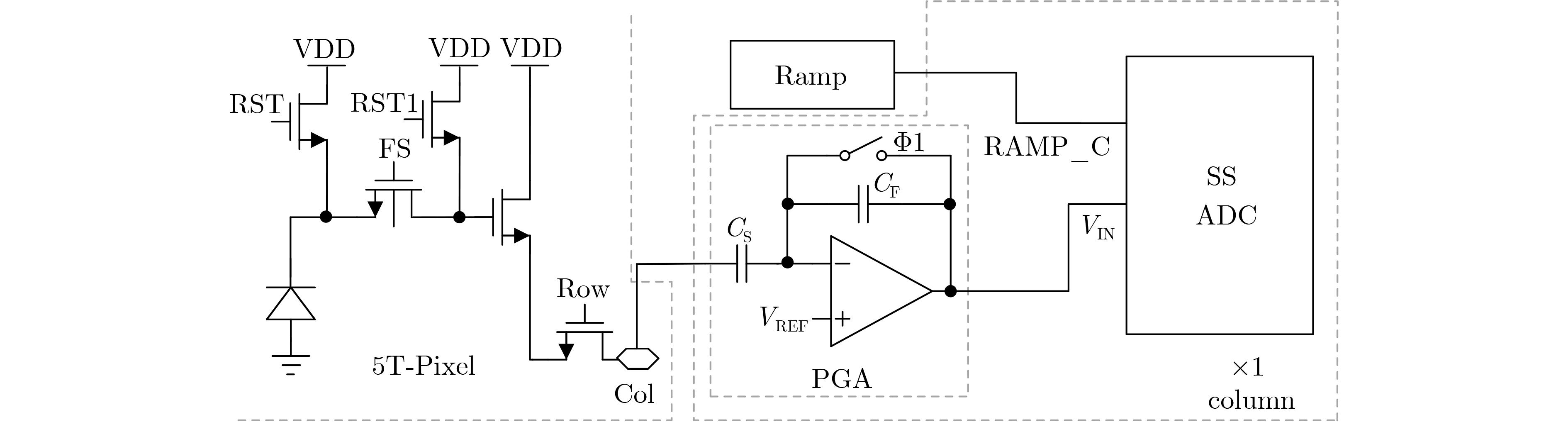
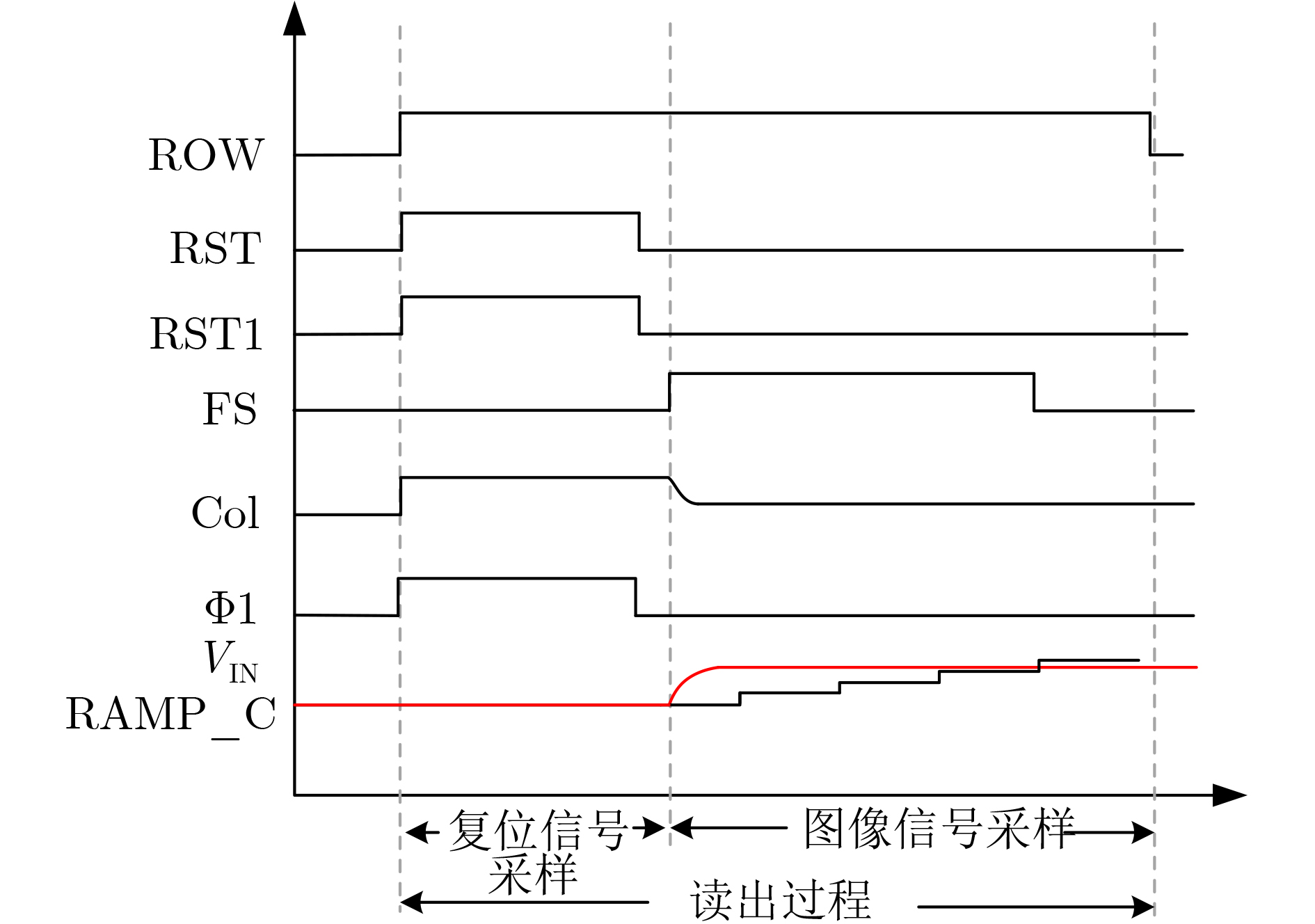
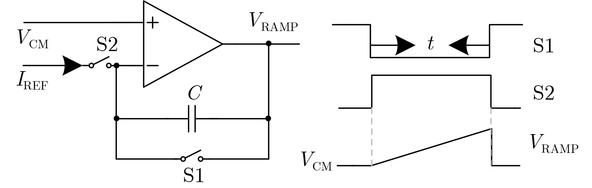
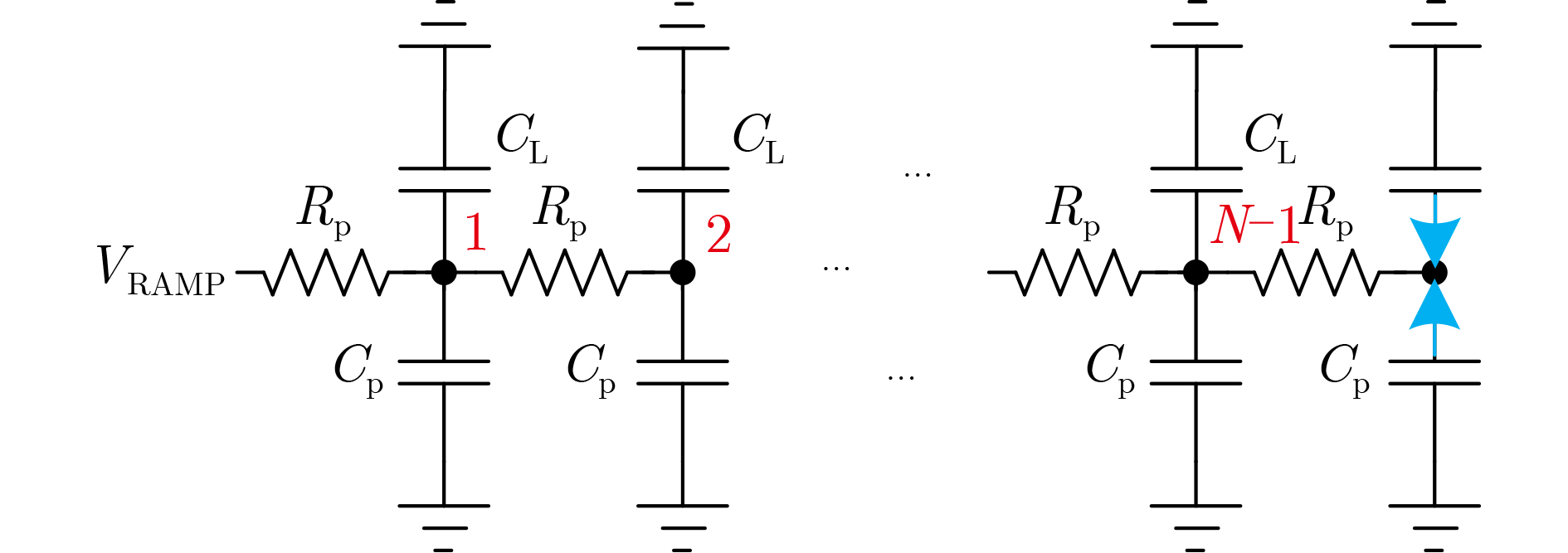
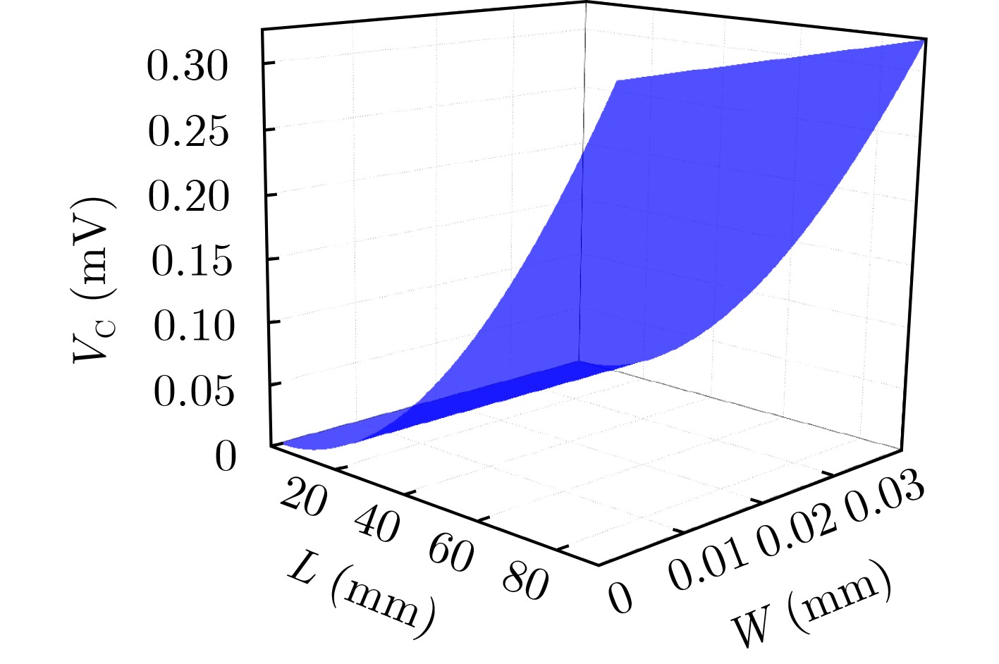
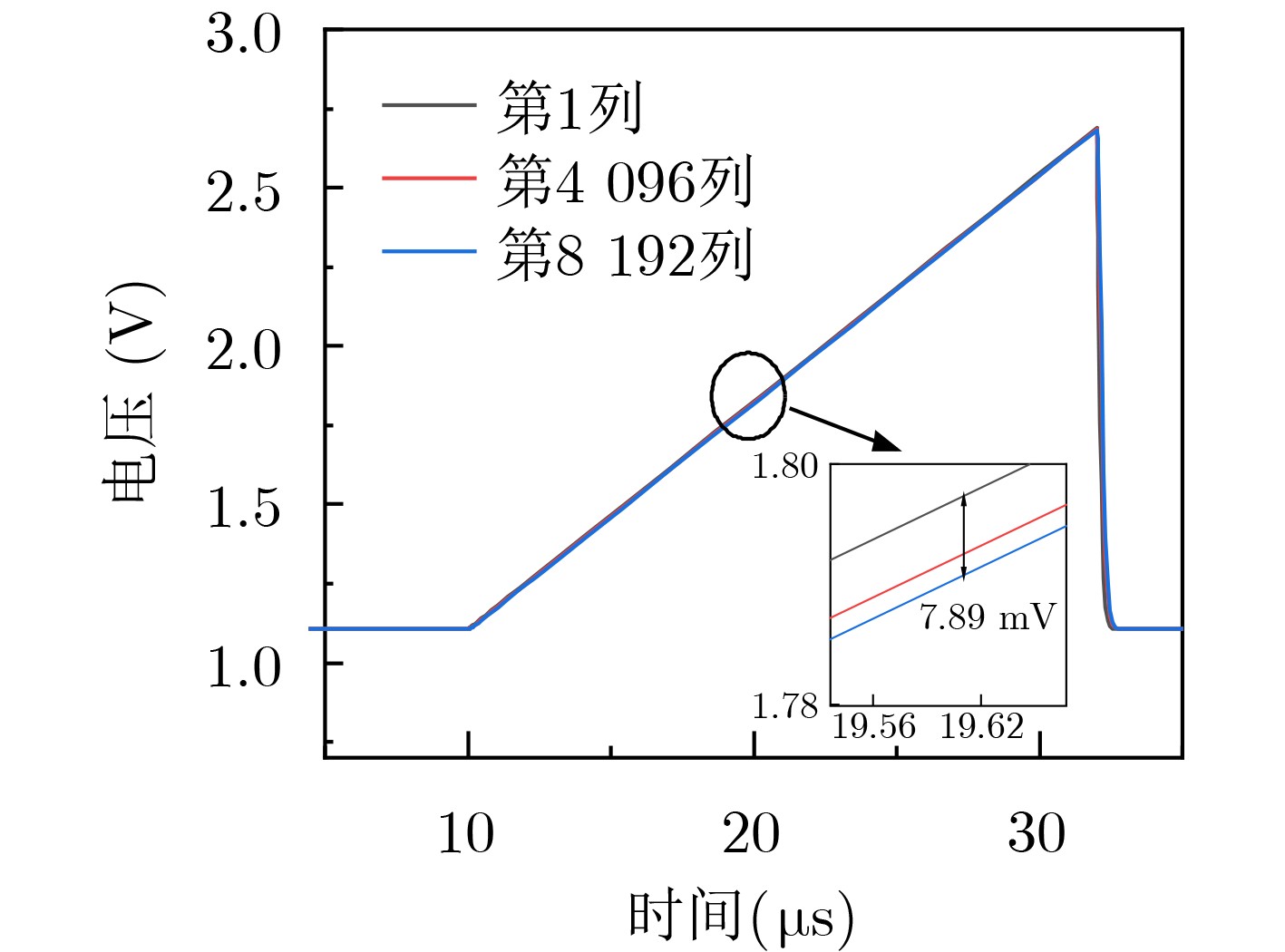
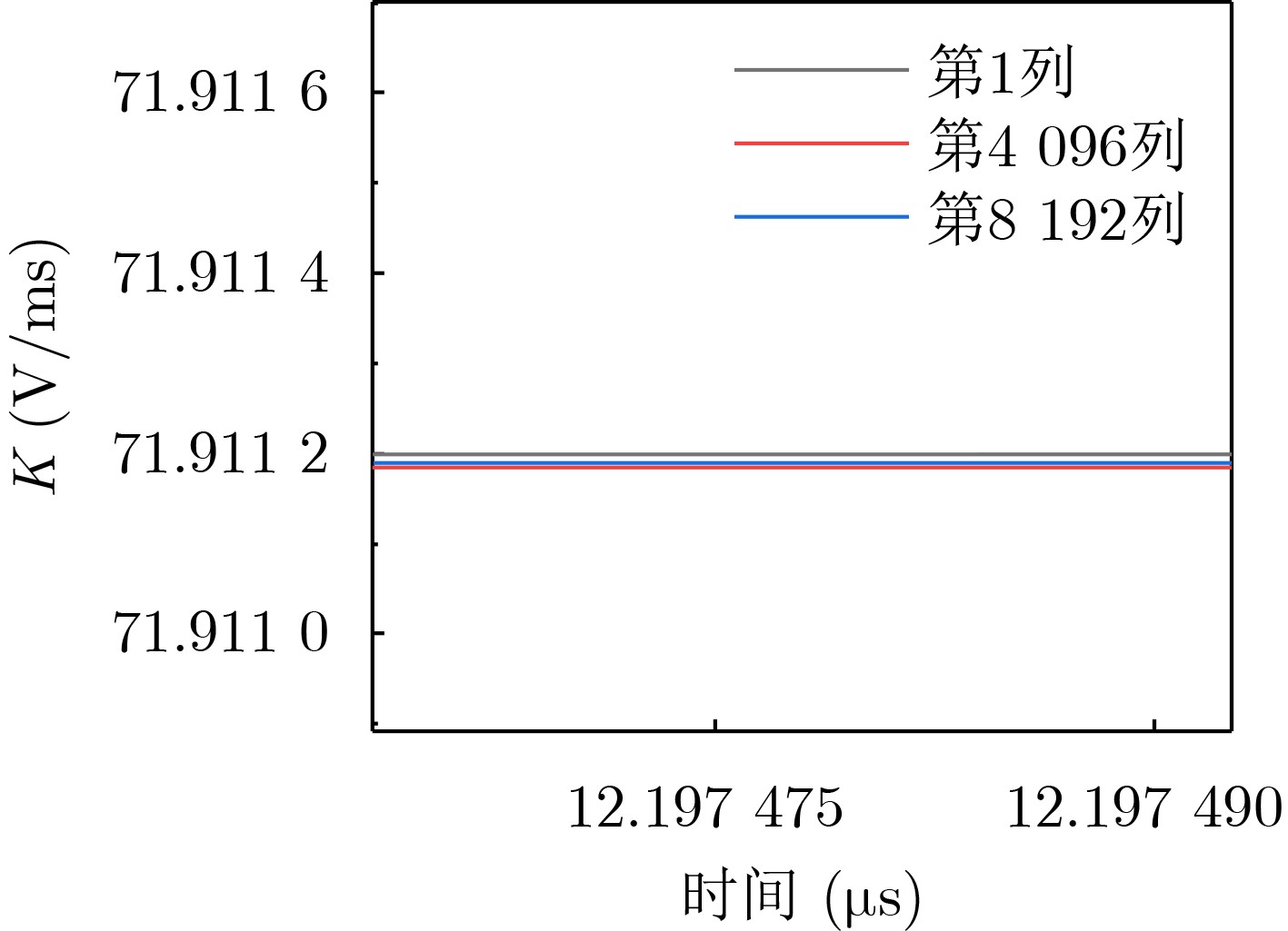
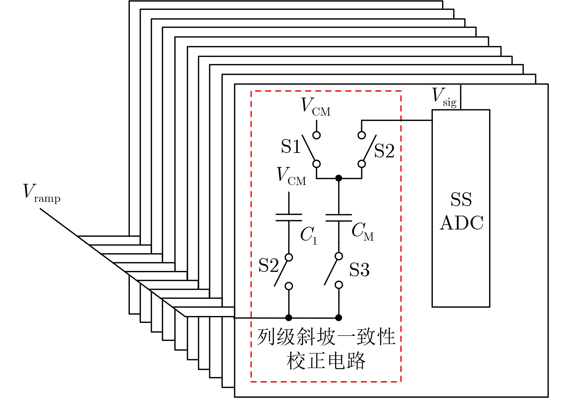
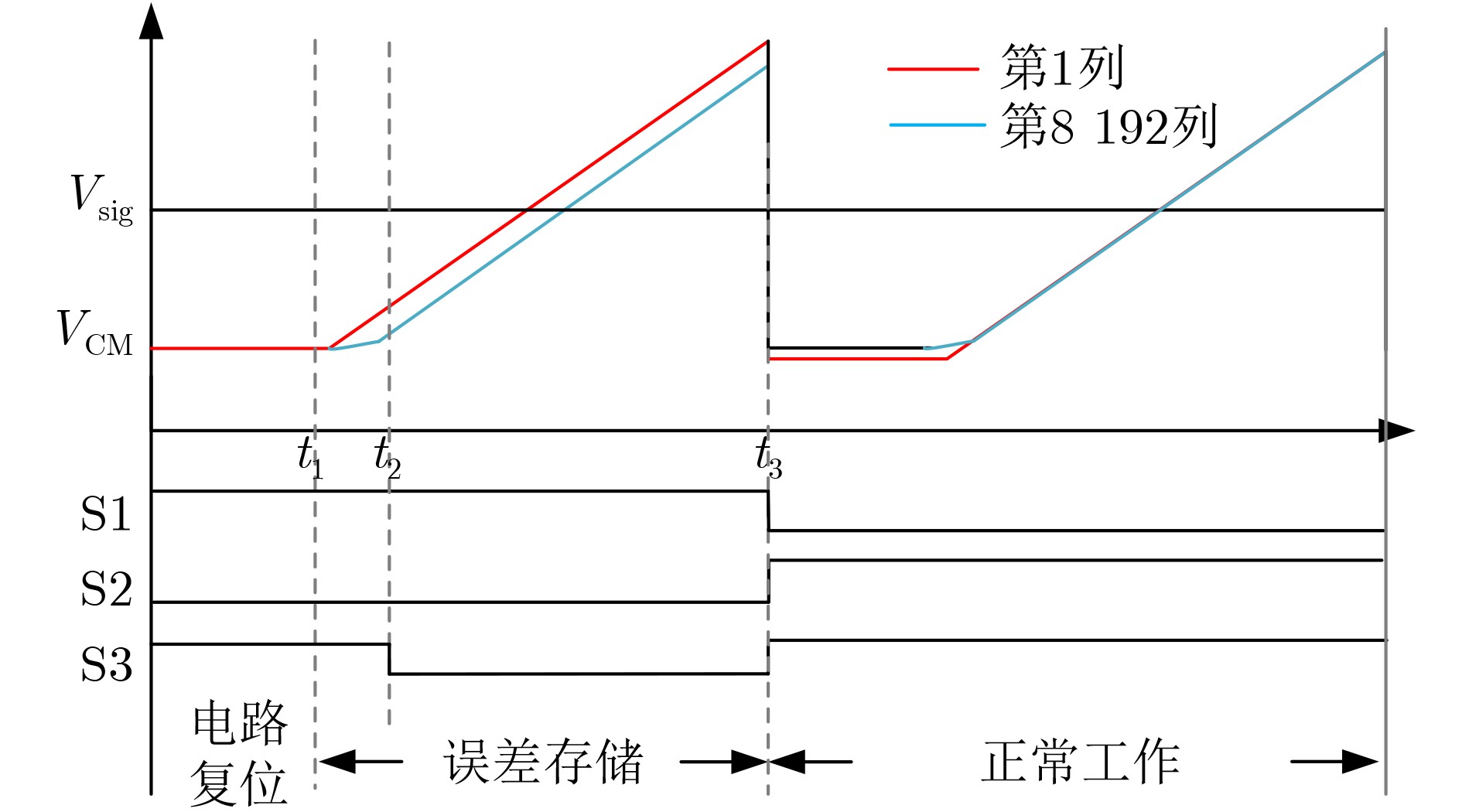
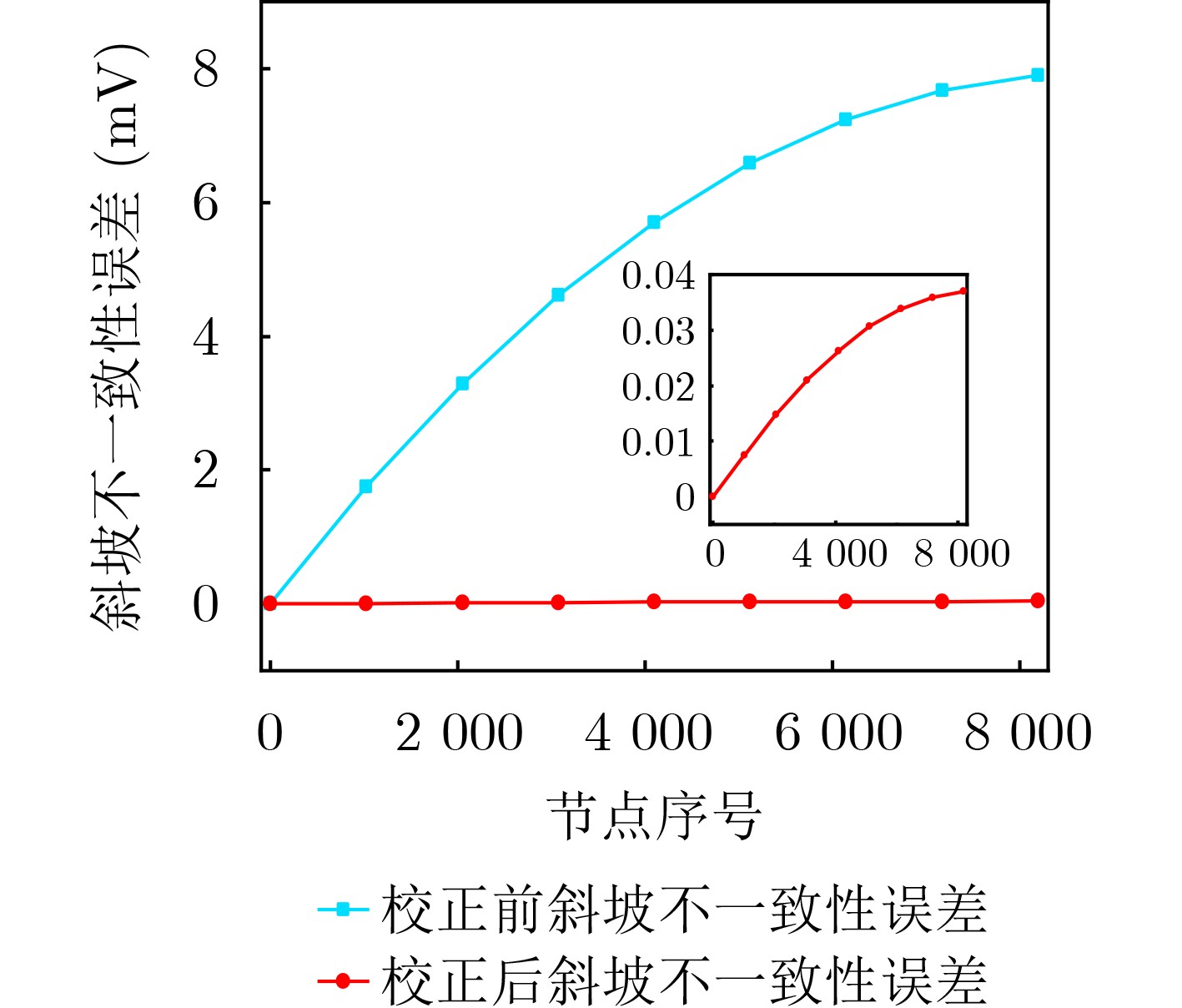
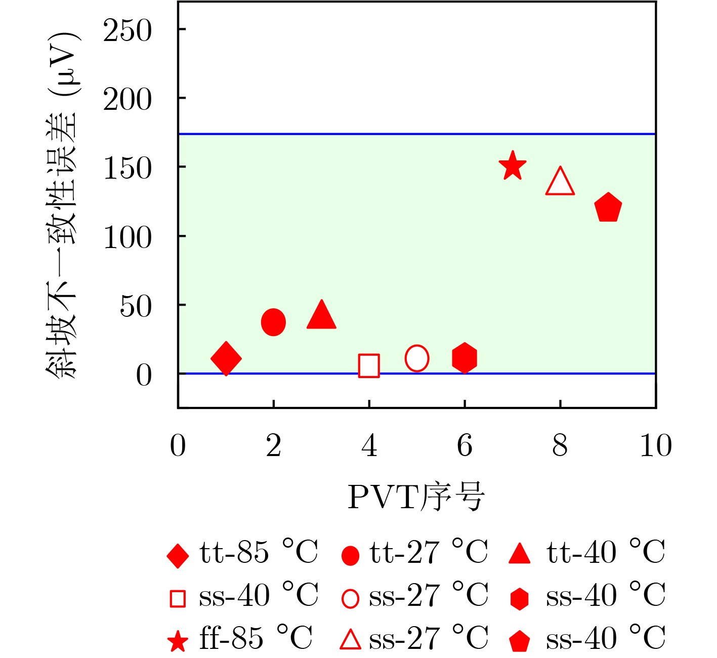
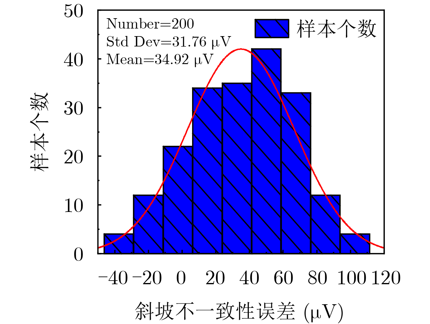
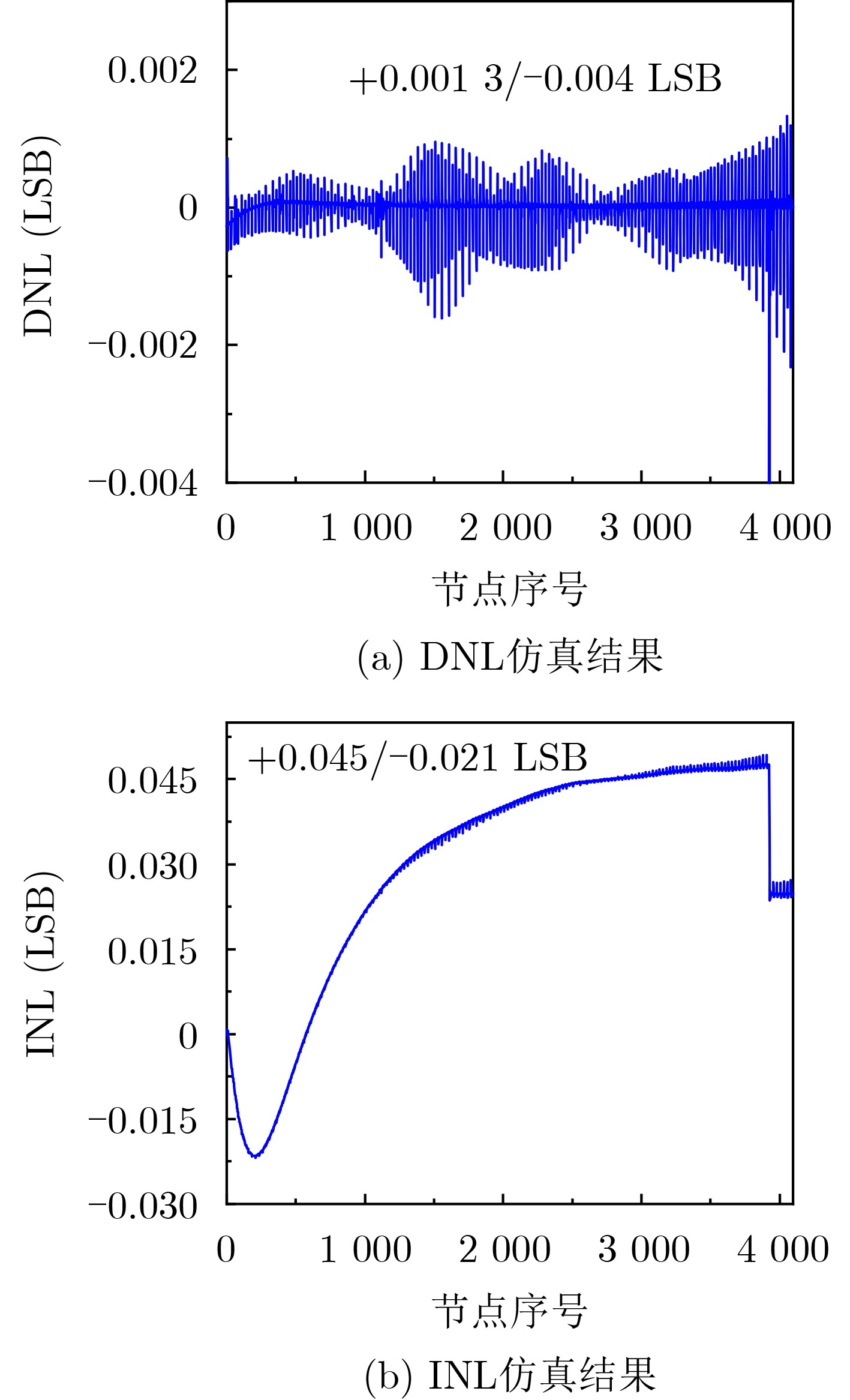
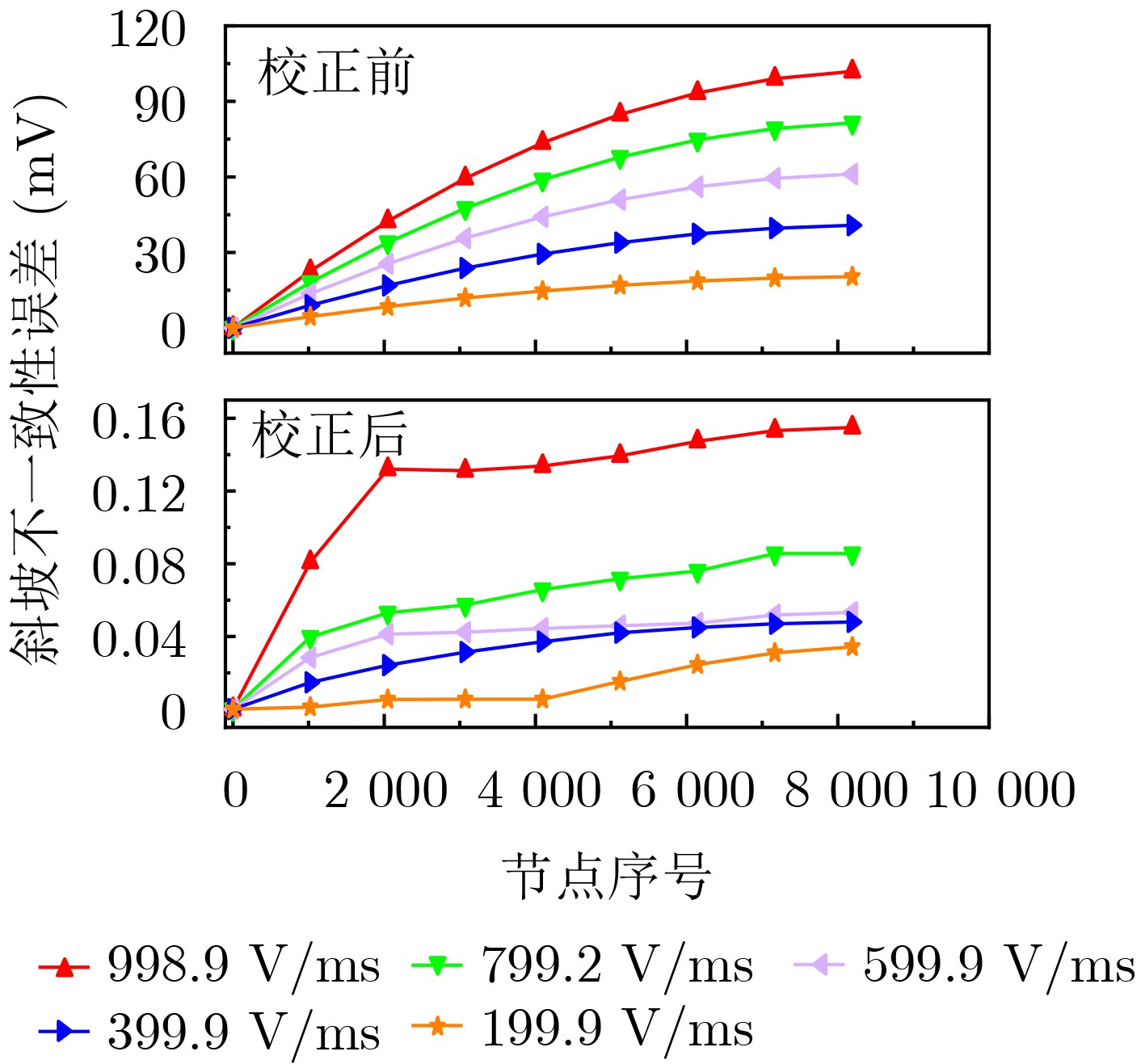
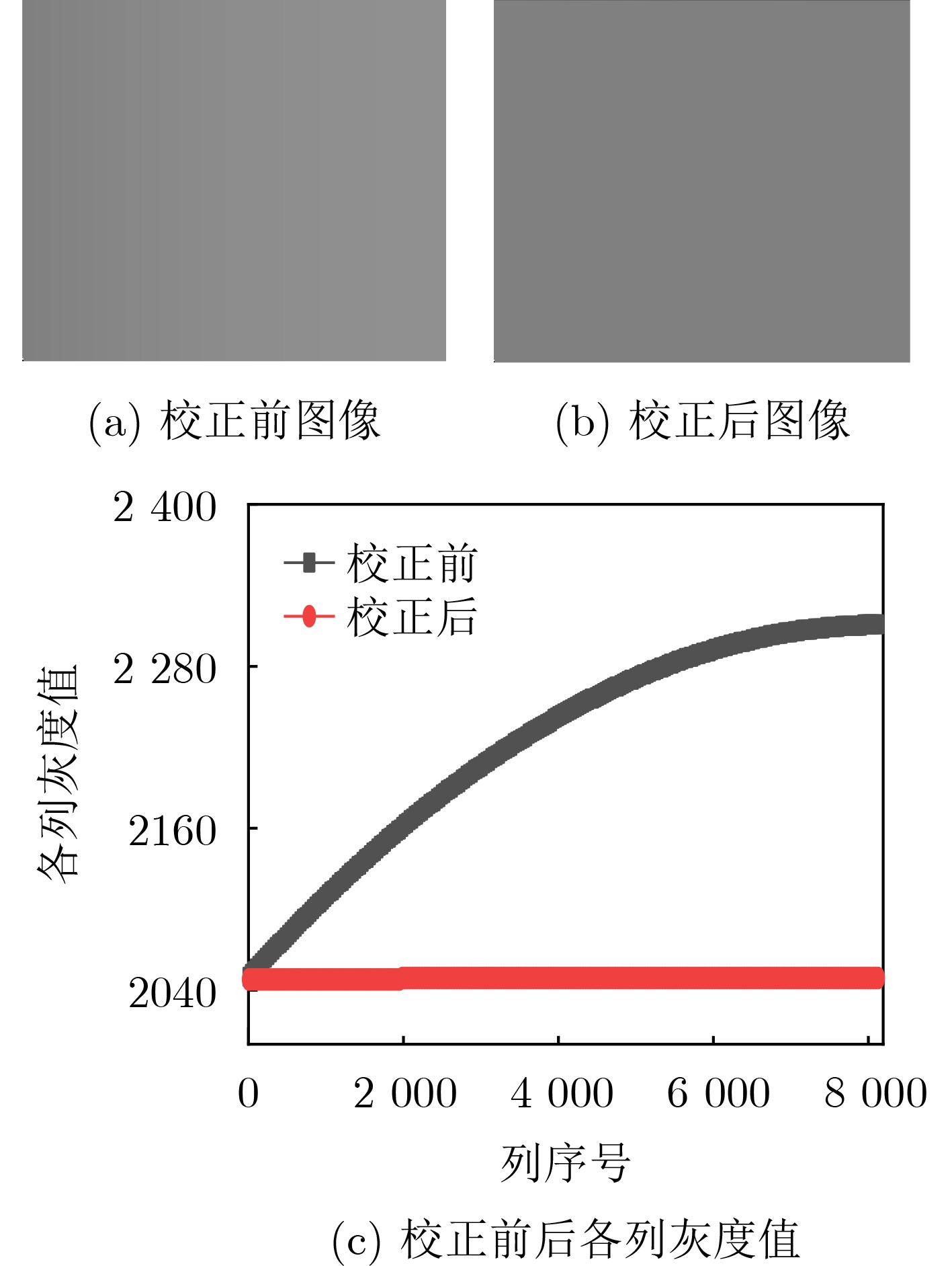
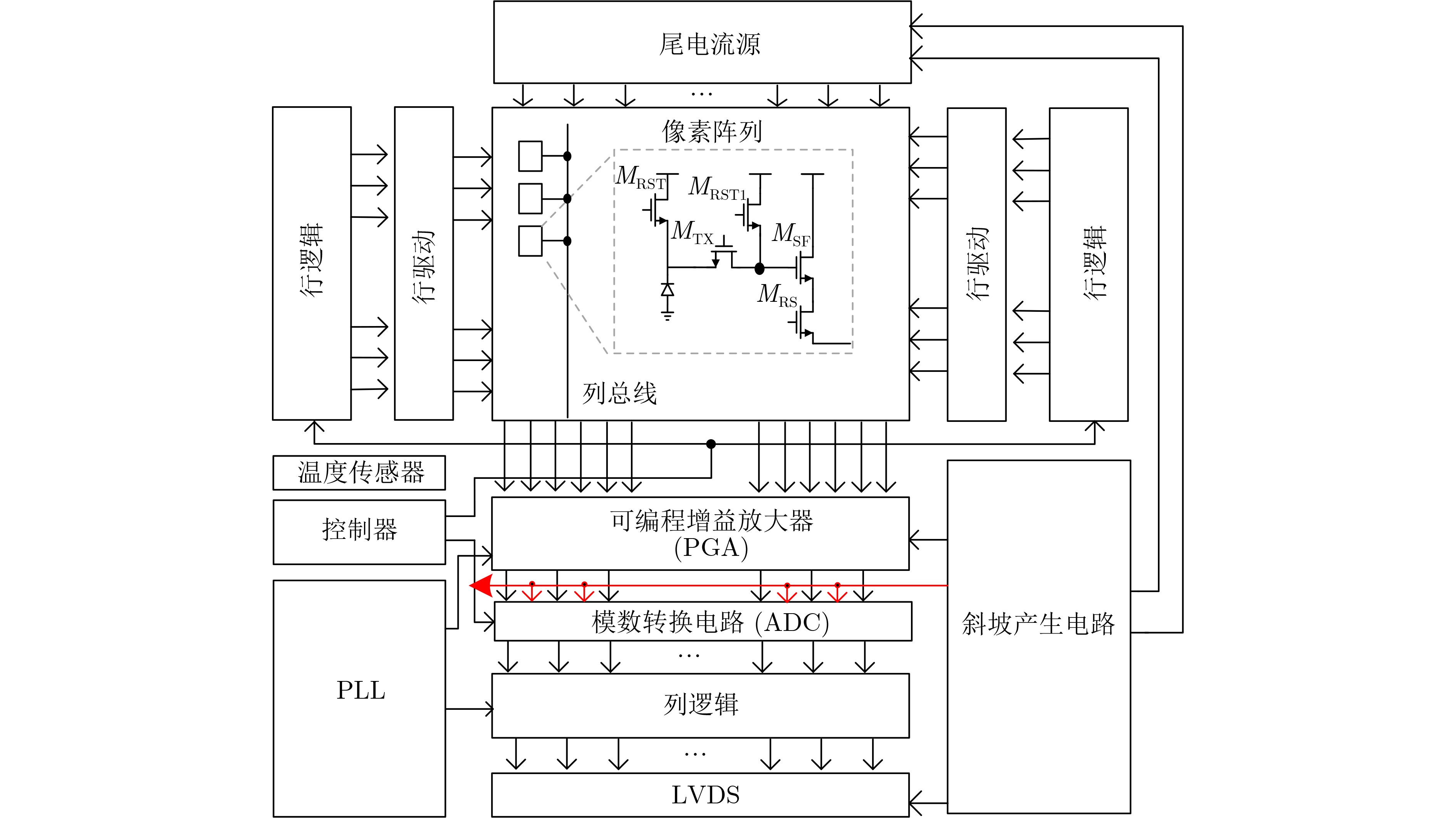
摘要: 针对大面阵CMOS图像传感器(CIS)中存在的斜坡信号不一致性问题,该文提出一种用于CMOS图像传感器的斜坡一致性校正方法。该误差校正方法基于误差存储和电平移位思想,在列级读出电路中引入用于存储各列斜坡不一致性误差的存储电容,根据存储的斜坡不一致性误差对各列的斜坡信号进行电平移位,确保斜坡信号的一致性。该文基于55 nm 1P4M CMOS工艺对提出的斜坡一致性校正方法完成了详细电路设计和全面仿真验证。在斜坡信号电压范围为1.4 V,斜坡信号斜率为71.908 V/ms,像素面阵规模为8 192(H)×8 192(V),单个像素尺寸为10 μm的设计条件下,该文提出的校正方法将斜坡不一致性误差从7.89 mV降低至36.8 μV。斜坡信号的微分非线性(DNL)为 +0.0013/–0.004 LSB,积分非线性(INL)为+0.045 /–0.02 LSB,列级固定模式噪声(CFPN)从1.9%降低到0.01%。该文提出的斜坡一致性校正方法在保证斜坡信号高线性度,不显著增加芯片面积和不引入额外功耗的基础上,斜坡不一致性误差降低了99.54%,为高精度CMOS图像传感器的设计提供了一定的理论支撑。Abstract: Considering the problem of the non-uniformity of the ramp signal in the large-array CMOS Image Sensors (CIS), a ramp uniformity correction method for CMOS image sensors is proposed in this paper. The correction method is based on error storage and level shift ideas. Storage capacitor that are used to store ramp non-uniformity error are introduced in column readout circuit. According to the stored ramp non-uniformity error, the ramp signal of each column is shifted. So as to ensure the uniformity of the ramp signal. Based on the 55 nm 1P4M CMOS process, this paper has completed the detailed circuit design and comprehensive simulation verification of the proposed method. Under the design conditions that the voltage range of the ramp signal is 1.4 V, the slope of the ramp signal is 71.908 V/ms, the number of pixel area arrays is 8192(H)×8192(V), and a single pixel size is 10 μm, the proposed correction method reduces the ramp non-uniformity error from 7.89mV to 36.8 μV. The Differential NonLinearity (DNL) of the ramp signal is +0.001 3/–0.004 LSB and the Integral NonLinearity (INL) is +0.045/–0.02 LSB. The Column Fixed Pattern Noise(CFPN) is reduced from 1.9% to 0.01%. The proposed ramp uniformity correction method reduces the ramp non-uniformity error by 99.54% on the basis of ensuring the high linearity of the ramp signal, without significantly increasing the chip area and without introducing additional power consumption. It provides a certain theoretical support for the design of high-precision CMOS image sensors.
-
[1] GUO Zhongjie, WANG Bin, LIU Suiyang, et al. High-linearity and high-speed ROIC of ultra-large array infrared detectors based on adaptive compensation and enhancement[J]. Sensors, 2023, 23(12): 5667. doi: 10.3390/s23125667 [2] ARAI T, YASUE T, KITAMURA K, et al. A 1.1 μm 33-mpixel 240-fps 3-D-stacked CMOS image sensor with three-stage cyclic-cyclic-SAR analog-to-digital converters[J]. IEEE Transactions on Electron Devices, 2017, 64(12): 4992–5000. doi: 10.1109/TED.2017.2766297 [3] GUO Zhongjie, CHENG Xinqi, XU Ruiming, et al. A 1Gpixel 10FPS CMOS image sensor using pixel array high-speed readout technology[J]. Integration, 2023, 89: 114–122. doi: 10.1016/j.vlsi.2022.12.002 [4] LEE J, PARK H, SONG B, et al. High frame-rate VGA CMOS image sensor using non-memory capacitor two-step single-slope ADCs[J]. IEEE Transactions on Circuits and Systems I:Regular Papers, 2015, 62(9): 2147–2155. doi: 10.1109/TCSI.2015.2451791 [5] GUO Zhongjie, WANG Yangle, XU Ruiming, et al. High-speed fully differential two-step ADC design method for CMOS image sensor[J]. Sensors, 2023, 23(2): 595. doi: 10.3390/s23020595 [6] XU Ruiming, GUO Zhongjie, YU Ningmei, et al. A high-speed 13-bit two-step single-slope ADC for large array CMOS image sensors[J]. Integration, 2023, 91: 119–125. doi: 10.1016/j.vlsi.2023.03.009 [7] IMAI K, YASUTOMI K, KAGAWA K, et al. A distributed ramp signal generator of column-parallel single-slope ADCs for CMOS image sensors[J]. IEICE Electronics Express, 2012, 9(24): 1893–1899. doi: 10.1587/elex.9.1893 [8] GUO Zhongjie, YU Ningmei, and WU Longsheng. A self-compensated approach for ramp kickback noise in CMOS image sensor column parallel single slope ADC[J]. Microelectronics Journal, 2022, 120: 105364. doi: 10.1016/j.mejo.2022.105364 [9] NOORWALI A A, QASIM S M, DOOST A S, et al. A 16-bit 4 MSPS DAC for lock-in amplifier in 65nm CMOS[C]. 2016 IEEE 13th International Conference on Networking, Sensing, and Control (ICNSC), Mexico City, Mexico, 2016: 1–5. [10] CHENG Xu, ZENG Xiaoyang, and FENG Qi. Analysis and improvement of ramp gain error in single-ramp single-slope ADCs for CMOS image sensors[J]. Microelectronics Journal, 2016, 58: 23–31. doi: 10.1016/j.mejo.2016.10.006 [11] DUMITRU F S, ILIE C R, and ENACHESCU M. Exploring the effect of segmentation on INL and DNL for a 10-bit DAC[C]. 2020 International Semiconductor Conference (CAS), Sinaia, Romania, 2020: 161–164. [12] SANKAR R S P, ASISH L, and BHUVAN B. Design of stable error-correction ramp generators considering process and run-time variations[C]. 2019 IEEE Asia Pacific Conference on Circuits and Systems (APCCAS), Bangkok, Thailand, 2019: 257–260. [13] NIE Kaiming, ZHA Wanbin, SHI Xiaolin, et al. A single slope ADC with row-wise noise reduction technique for CMOS image sensor[J]. IEEE Transactions on Circuits and Systems I:Regular Papers, 2020, 67(9): 2873–2882. doi: 10.1109/TCSI.2020.2979321 [14] SAITO W, IIZUKA Y, KATO N, et al. A low noise and linearity improvement CMOS image sensor for surveillance camera with skew-relaxation local multiply circuit and on-chip testable ramp generator[C]. 2021 IEEE Asian Solid-State Circuits Conference (A-SSCC), Busan, Korea, 2021: 1–3. [15] GUO Zhongjie, YU Ningmei, and WU Longsheng. Research on column FPN and black level calibration in large array CMOS image sensor[J]. Chinese Journal of Electronics, 2021, 30(2): 268–274. doi: 10.1049/cje.2021.02.004 [16] LEE J, BAEK I, YANG D, et al. On-chip FPN calibration for a linear-logarithmic APS using two-step charge transfer[J]. IEEE Transactions on Electron Devices, 2013, 60(6): 1989–1994. doi: 10.1109/TED.2013.2259236 [17] LIU Zhenwang, XU Jiangtao, WANG Xinlei, et al. A fixed-pattern noise correction method based on gray value compensation for TDI CMOS image sensor[J]. Sensors, 2015, 15(9): 23496–23513. doi: 10.3390/s150923496 [18] CHEN Ming, ZHOU Li, YANG YangJun, et al. A 15.5x-gain 0.29-mm2 CMOS readout circuit for 1.5-Mpixel 60-fps CMOS image sensor[J]. Analog Integrated Circuits and Signal Processing, 2021, 108(1): 89–99. doi: 10.1007/s10470-020-01778-8 [19] 郭仲杰, 王杨乐, 许睿明, 等. 应用于CMOS图像传感器的高速全差分两步式ADC设计方法[J]. 电子与信息学报, 2023, 45(9): 3410–3419. doi: 10.11999/JEIT221420GUO Zhongjie, WANG Yangle, XU Ruiming, et al. high-speed fully differential two-step ADC design method for CMOS image sensor[J]. Journal of Electronics & Information Technology, 2023, 45(9): 3410–3419. doi: 10.11999/JEIT221420 [20] KIM H J. 11-bit column-parallel single-slope ADC with first-step half-reference ramping scheme for high-speed CMOS image sensors[J]. IEEE Journal of Solid-State Circuits, 2021, 56(7): 2132–2141. doi: 10.1109/JSSC.2021.3059909 [21] PARK W, PIAO Canxing, LEE H, et al. CMOS image sensor with two-step single-slope ADCs and a detachable super capacitive DAC[J]. IEEE Transactions on Circuits and Systems II:Express Briefs, 2022, 69(3): 849–853. doi: 10.1109/TCSII.2021.3118647 -

 下载:
下载:

图(18) / 表(1)
计量
- 文章访问数: 55
- HTML全文浏览量: 20
- PDF下载量: 12
- 被引次数: 0
